Abstract
This article presents a neural network-based control method for maintaining the required output voltage of a synchronous buck converter. The goal was to replace a traditional PID controller with a neural network that calculates the duty cycle based on real-time data. Several versions of the neural network were tested. The final version, which included the input voltage, reference, and output current as inputs and compensated for dead time, was successfully validated on real hardware. It was able to respond to changes in load and input voltage within a limited operating range.
1. Introduction
Artificial neural networks are gradually becoming an integral part of modern life, with a wide range of practical applications. They are used in areas such as computer vision, speech recognition, and text processing and are increasingly applied in industrial sectors, including robotics, chemical processes, control systems, and power electronics. Power semiconductor converters are an integral part of modern electronic systems designed to convert electrical energy. These devices control the flow of energy between a source and a load, thereby ensuring the required transformation of voltage or current levels. The key component of any power converter is its control circuit. Figure 1 shows the basic block diagram of the power converter control circuit.
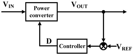
Figure 1.
A block diagram of a standard power converter control circuit.
One of the most widely used control techniques in the field of power converters is pulse-width modulation, the principle of which is to control the duty cycle (D) of the switching signal for semiconductor elements. By changing the duty cycle, the output voltage can be precisely adjusted. In conventional closed control loops, classic PID controllers are often used for this purpose. Since PID controllers were originally designed for linear systems, their application to nonlinear systems such as power converters has certain limitations. Therefore, much research interest is focused on the development of new, more sophisticated control methods. One such alternative is neural networks.
The application of neural networks in power converter control has been the focus of numerous research studies, where these networks were implemented across various converter topologies [1,2,3,4,5,6]. These include not only rectifiers and a range of DC/DC converters but also inverters. In the case of buck converters, most studies concentrate on the basic (non-synchronous) variant [1,7,8], while very few address its synchronous version. Despite the volume of research, many of these works lack a detailed description of the neural network design process for specific applications. Often, only experimental results or suggested improvements are presented without a deeper explanation of the methodology used.
Furthermore, a large portion of the studies are limited to simulation analyses [5,9,10,11], with relatively few including results from real hardware experiments. It is also common for researchers to integrate neural networks with other control strategies, such as sliding mode control or model predictive control [12,13,14]. Beyond power converters, neural networks are also applied in other areas of electrical engineering [15,16].
Through gradual analysis and experimentation, a total of three neural networks were proposed in this work. Neural network 1 was trained based on the static voltage transfer characteristic of a buck converter. However, this approach proved ineffective in compensating for changes in the converter’s output load resistance. Specifically, the duty cycle remained unchanged when the output resistance varied.
To address this, neural network 2 was developed by including the output current of the converter as an additional input parameter. Simulation results for this network were promising, but during experimental testing, it failed to maintain the desired output voltage. After a mathematical analysis, it was found that incorporating dead time during the neural network training process is crucial. In this particular neural network, the dead time was not considered when collecting training data. However, in a real system, this safety time must be applied to prevent short circuits.
Finally, neural network 3 was introduced as a software improvement of neural network 2, involving modifications to relevant microcontroller registers to account for dead time. This final solution successfully achieved stable and reliable output voltage regulation in real-world operation and was selected as the definitive implementation.
2. Neural Networks
Neural networks are a modern machine learning tool inspired by the human brain. They are characterized by the ability to learn from previous experience and adapt to changing conditions. Their flexibility lies in the wide possibilities of configuring the topology (e.g., feedforward, recurrent, or modular architectures—Figure 2), the type of neurons used, activation functions (such as sigmoid, hyperbolic tangent, or ReLU), and other parameters.
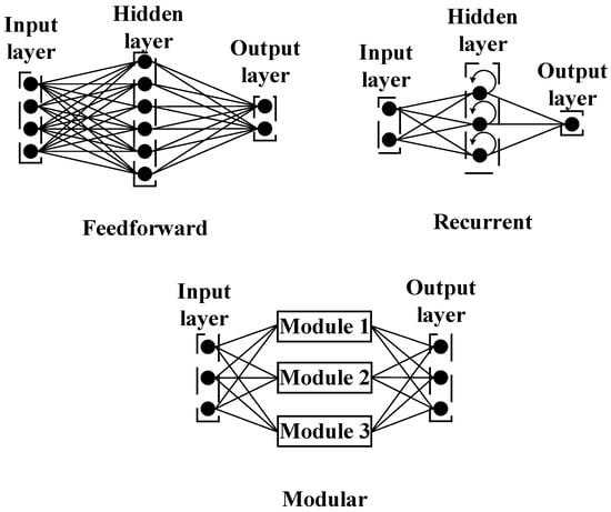
Figure 2.
Frequently used neural network architectures.
A feedforward neural network is one of the most fundamental types of neural network. In the field of power converters, this is typically the only type encountered. It consists of multiple neurons organized into layers—specifically, an input layer, one or more hidden layers, and an output layer.
Recurrent neural networks are commonly used for tasks such as text translation, speech recognition, or subtitle generation. However, in the field of power converter control, this type of neural network is rarely utilized [17].
The modular structure of a neural network enables its application to more complex tasks. It consists of several interconnected modules, where each module tackles a smaller subtask of the overall problem. These modules can be thought of as individual neural networks, each responsible for solving a specific portion of the main task [18].
The basic building block of a neural network is an artificial neuron. The principle of a neuron is shown in Figure 3. As can be seen, a neuron has several inputs and one output. The number of inputs can be flexible and depends on the requirements of the given application. Each neuron is characterized by a parameter known as a weight. The weight is a real number that indicates the priority of a given neuron.
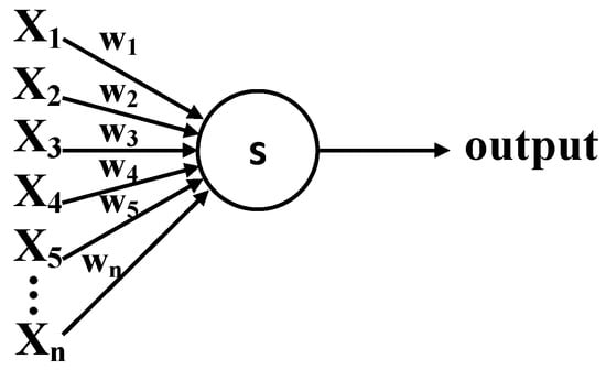
Figure 3.
Artificial neuron.
The output of the perceptron is determined by a simple rule. The threshold value is a real number that the weighted sum must reach for the neuron to be active and send the signal on. If the weighted sum s—the sum of the products of the input values and their respective weights—is less than the threshold value, then the output is 0. Conversely, if the weighted sum is greater than the threshold value, the output of the neuron is equal to 1 [19,20].
Weighted sum:
A simplified description of a neuron is often given in the literature, where a scalar product replaces the weighted sum:
where
- w is the weight vector;
- x is the vector of inputs.
Another common modification is to replace the threshold value in the neuron output calculation with the so-called bias value b. As a result, the description of the neuron can be adjusted according to Equation (4) [19].
The main disadvantage of such a neuron is its inability to learn. In neural network training, small changes in weights and biases must result in only small changes in the network’s output. However, a binary-output neuron can respond disproportionately to such small changes, causing its output to switch abruptly from 0 to 1 or vice versa. This abrupt behavior can lead to a complete change in the overall behavior of the neural network. To address this limitation, an activation function is introduced. The key difference is that the neuron’s output is no longer binary but can take on continuous values, typically in the range from 0 to 1. The most commonly used activation functions are shown in Figure 4 [19,21].
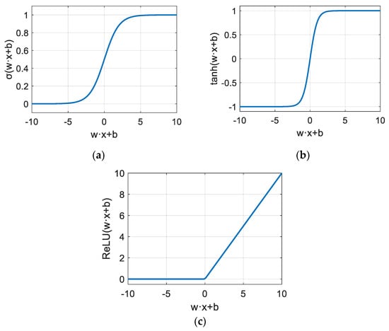
Figure 4.
Common activation functions in neural networks: (a) sigmoid; (b) hyperbolic tangent; (c) ReLU.
3. Neural Network Design
In this case, the MATLAB (R2025a) simulation environment was used for the design and training of the neural network, as it offers an extensive toolbox for working with neural networks. This tool provides broad capabilities for creating, training, and testing various types of neural networks. It supports detailed tuning and experimentation with multiple parameters such as network architecture, training algorithms, activation functions, and other adjustable settings, thereby enabling flexibility in optimizing the designed solution.
Another significant advantage of this environment is the ability to verify the functionality and required properties of the designed neural network directly in Simulink. In the context of power converters, this enables testing the neural network on a simulation model of the converter, allowing assessment of whether it can deliver the desired control performance.
The BOOSTXL-BUCKCONV development kit from Texas Instruments (TI), whose schematic is shown in Figure 5, was selected as the model of the synchronous buck converter for which the neural network was designed and trained. This choice was motivated by its compatibility with TI’s C2000-class microcontroller development kits. Since this is a synchronous buck converter, it is essential to set an appropriate safety time for the control signals to prevent short circuits in the circuit. As will be shown, this safety time also significantly affects the performance of the neural network and therefore must be considered even in simulation analyses.
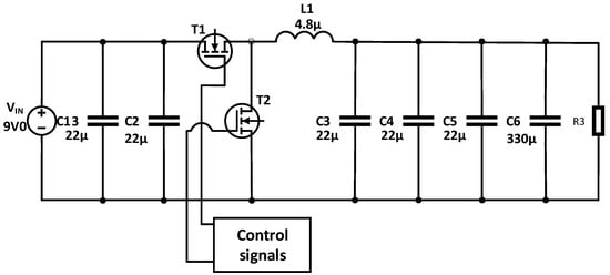
Figure 5.
A schematic of the BOOSTXL-BUCKCONV synchronous buck DC/DC converter.
Feedforward neural networks are commonly used in power electronics and electrical engineering, which is why this type was selected in this case. This network type is well-suited for modeling nonlinearities, making it appropriate for the application. Another key advantage is its simple topology, which significantly reduces the required computational power, particularly on standard microcontrollers. The neural network was programmed in the TMS320F28069M microcontroller (TI, Dallas, TX, USA).
3.1. Neural Network 1
In the field of power converters, feedforward neural networks are most commonly used; therefore, this architecture was chosen in this case as well. Initially, the neural network is trained to ensure a stable output voltage under various fault conditions, based on the transfer characteristic of the buck converter defined by Equation (5), which is expressed as the ratio of the output voltage to the input voltage.
Since the neural network’s task is to accurately determine the duty cycle, it is logical that this will be its output parameter. Therefore, the output layer of the proposed network contains only one neuron. Based on Equation (5), the input and output voltages are used as inputs to the network, which results in two neurons in the input layer. The number of hidden layers and neurons can vary depending on the specific requirements of the application. In this case, the hidden-layer structure was set to [5, 5]. The overall architecture of the network is illustrated in Figure 6, where the hidden layers are shown for illustrative purposes only.
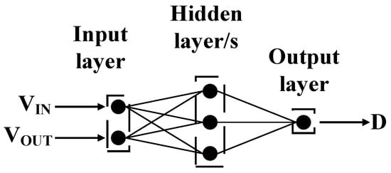
Figure 6.
An illustrative diagram of the proposed neural network 1 structure.
Initial tests with this neural network revealed significant shortcomings. Network 1 designed in this manner was unable to maintain the required voltage and could not provide regulation under fault conditions. A more detailed analysis showed that the network operates correctly only when a reference signal is fed to its input instead of the output voltage, as illustrated in Figure 7.
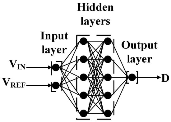
Figure 7.
Modified neural network 1 structure.
The neural network structure, as modified, was able to provide the required output voltage. The output voltage curve under nominal conditions is shown in Figure 8, with the steady-state value reaching 1.985 V. The required reference voltage was 2 V.
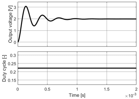
Figure 8.
Output voltage and duty cycle curves for nominal parameters—network 1.
Subsequently, the neural network’s ability to maintain the required output voltage under varying input voltage and load conditions was tested. Figure 9 shows the output voltage curve when the input voltage changed from 9 V to 15 V. As observed, the neural network responded adequately to this change by adjusting the duty cycle accordingly. The output voltage stabilized at 1.99 V.
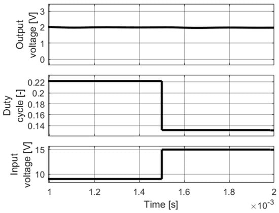
Figure 9.
Output voltage and duty cycle during input voltage step change (9 V to 15 V).
Simulation analysis showed that this neural network handled various input voltage values well and adjusted the duty cycle accordingly. However, problems arose when testing the network’s ability to compensate for changes in load. As shown in Figure 10 and in detail in Figure 11, when the load resistance changed from 7.5 Ω to 4 Ω, the output voltage dropped below the required reference of 2 V, measuring 1.97 V. At even lower load resistances, this deviation increased further. From the figure, it is evident that the cause of this issue is that the neural network did not adjust the duty cycle in response to changes in load resistance.
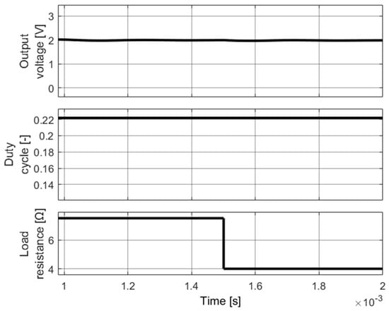
Figure 10.
Output voltage and duty cycle during load resistance step change—Neural network 1 (7.5 Ω to 4 Ω).
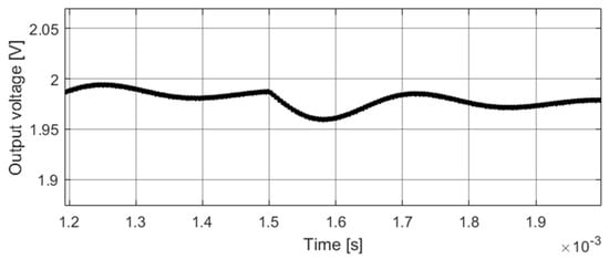
Figure 11.
Detail of the output voltage when the load changed from 7.5. Ω to 4 Ω.
The analysis shows that this neural network is able to adjust the duty cycle only under one type of fault condition: when the input voltage changes. However, it fails to do so when the load changes. This indicated that the structure of the designed network 1 needs to be modified, likely by adding additional input parameters. Since the network was unable to react to load variations, the most appropriate solution would be to include another output-related variable, such as current or voltage, among the inputs.
3.2. Neural Network 2
For this case, the structure of neural network 1 was modified by adding the converter’s output current to its input parameters, which, of course, led to an increase in the number of neurons in the input layer. The modified structure is shown in Figure 12. Following the simulation analysis, the number of hidden neurons was reduced to the minimum necessary, resulting in a hidden-layer structure of [4, 3], which was still capable of achieving the required control performance. However, further reduction in the number of hidden neurons led to increased deviation of the output voltage from the desired reference.
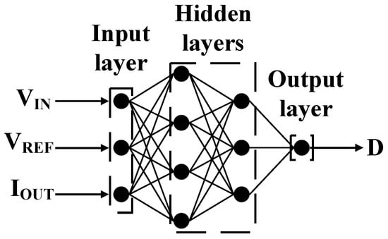
Figure 12.
Modified structure of neural network 1—network 2.
Figure 13 shows the output voltage and duty cycle curves under nominal conditions. Unlike network 1, which applied a constant duty cycle value and maintained it, this network actively responded to changes in the output voltage. The output voltage stabilized at 1.98 V.
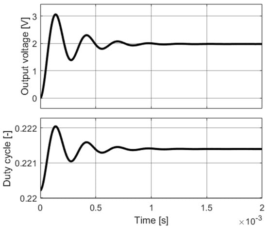
Figure 13.
Output voltage and duty cycle for nominal values—network 2.
In this case, it was also necessary to test the ability of the designed network to regulate step changes in both the load and input voltage. As shown in Figure 14, the neural network was able to adapt the duty cycle value when the input voltage changed, as well as network 1. This figure presents the output voltage curve during an increase in input voltage from 9 V to 11 V, with only minimal overshoot of approximately 30 mV. Figure 15 provides a detailed view of the output voltage response during this change. The output voltage stabilized at 2.015 V.
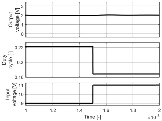
Figure 14.
Output voltage and duty cycle during input voltage step change (9 V to 11 V).
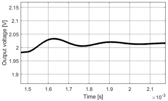
Figure 15.
Detail of the output voltage when the input voltage changed from 9 V to 11 V.
This network was able to regulate the output voltage acceptably within the input voltage range of 2 V to 11 V. At voltages above 11 V, however, it was unable to maintain the required reference value, with regulation deviations reaching several hundred millivolts in some cases.
The waveform shown in Figure 16 illustrates the output voltage response to a change in load resistance. It is immediately apparent that this network is capable of regulating such changes. Unlike network 1, which was unable to adjust the duty cycle and remained constant during load variations, this network responded accordingly. The output voltage waveform for a step change in load resistance from 7.5 Ω to 4 Ω is shown here, with a detailed view provided in Figure 17. In this case, the output voltage stabilized at 1.98 V. Similarly, in Figure 18, and shown in more detail in Figure 19, when the load resistance was changed from 7.5 Ω to 1.3 Ω, the output voltage stabilized at 1.98 V.
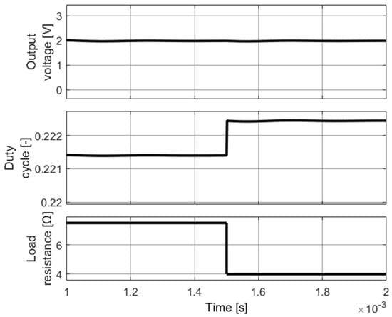
Figure 16.
Output voltage and duty cycle during load resistance step change—Neural network 2 (7.5 Ω to 4 Ω).
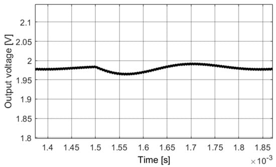
Figure 17.
Detail of the output voltage when the load resistance changed from 7.5 Ω to 4 Ω.
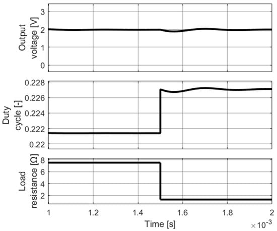
Figure 18.
Output voltage and duty cycle during load resistance step change (7.5 Ω to 1.3 Ω).
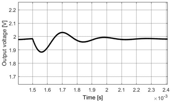
Figure 19.
Detail of the output voltage when the load resistance changed from 7.5 Ω to 1.3 Ω.
However, this network also exhibits certain limitations. During an increase in load resistance, it maintained similar regulation behavior regardless of the specific resistance value. When the resistance decreased, it was able to maintain the required voltage with minimal overshoot down to a resistance of 2 Ω. At lower resistance values, the overshoot reached several hundred millivolts. Nevertheless, the network was still able to achieve the desired output voltage, even at very low load resistance values in the range of tens of milliohms, albeit with significantly higher overshoot. For example, when the load dropped to 50 mΩ, the overshoot reached approximately 1.4 V, and the settling time slightly exceeded 0.5 ms. Despite this, the output voltage eventually stabilized at 1.98 V.
4. Experimental Validation of Network 2
Experimental verification of the functionality of the proposed neural network 2 was carried out according to the schematic representation in Figure 20. As shown, the neural network takes the input voltage, reference, and output current as inputs. Determining the reference is straightforward in this case, as it can be defined by a simple constant within digital control. The BOOSTXL-BUCKCONV converter kit provides measurements of the input voltage, output voltage, and current through the inductor; however, only the input voltage measurement is usable for this application. Therefore, the kit was modified by replacing the original load resistor with a current sensor and an electronic load.
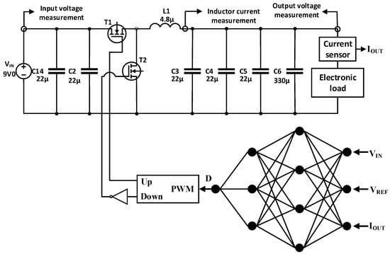
Figure 20.
A schematic representation of the neural network’s connection to the BOOSTXL-BUCKCONV kit.
Figure 21 shows the steady-state output voltage obtained using network 2. The measurement was performed under nominal conditions: an input voltage of 9 V, a reference voltage of 2 V, and an output resistance of 7.5 Ω. As shown, the steady-state output voltage matches neither the set reference value nor the simulation results. While the simulation predicted a voltage of 1.98 V under these conditions, the actual measurement showed only 1.79 V.
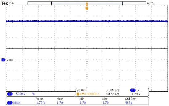
Figure 21.
Output voltage waveform at steady state using neural network 2.
A question remains: what causes the differences between the simulation and the real measurement? The most likely cause of this deviation is the dead time implemented in the PWM signals, since this is a synchronous buck converter. In this measurement, the dead time was set to 100 ns, as shown in Figure 22. This time delay could theoretically affect the results, as it was considered neither in the simulation used for generating the training data nor in the subsequent simulation to verify the network’s control performance.
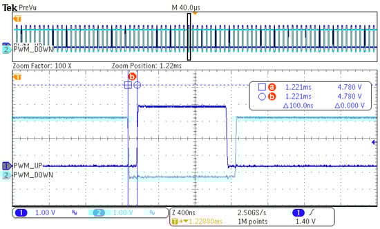
Figure 22.
A dead time of 100 ns was set in the PWM signals.
The system clock of the microcontroller operated at 90 MHz, while the converter’s switching frequency was set to 200 kHz. Since the UP–DOWN ePWM modulation mode was used, the TBPRD register value needed to be set to 225, as expressed by Equations (6) and (7) and illustrated in Figure 23.
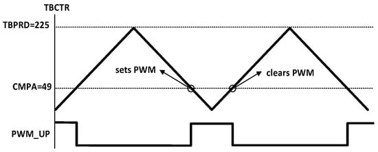
Figure 23.
The principle of operation of the ePWM peripheral registers.
In this measurement, the microcontroller calculated that the CMPA register value should be set to 49.9 to achieve the duty cycle determined by the neural network. However, because the standard ePWM module does not support fractional register values without the high-resolution extension (HRePWM), only the integer part of the value can be stored in the CMPA register. As a result, the value was rounded down to 49.
Although using HRePWM would allow for a more precise adjustment of the duty cycle, in reality, this would mean increasing the CMPA value by less than 1. This would result in extending the switching time of the upper transistor by less than one clock cycle, which would still be insufficient to achieve the desired output voltage of 2 V.
Since the value 49 was written to the CMPA register, the expected turn-on duration of the upper transistor was 1.09 µs, as shown in Equation (8).
However, as shown in Figure 24, the actual turn-on time of the upper transistor was only 990 ns, which means it was shortened by the dead time of 100 ns, as expressed in Equation (9).
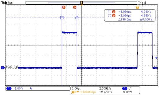
Figure 24.
The turn-on duration of the upper transistor when using neural network 2.
Subsequent mathematical analysis showed that, based on the values calculated by the neural network and assuming zero dead time, the converter’s output voltage would theoretically reach 2 V. The first step is to express the duty cycle based on these calculated values. In this case, it is assumed that any value, including decimal values, can be written to the CMPA register.
After the neural network calculated the required value, the result to be set in the CMPA register was 49.9. Since the ePWM operates in UP–DOWN mode, one ePWM period consists of 450 processor clock cycles. The number of clock cycles during which the upper transistor is switched on is given by 2CMPA.
This principle is evident from Figure 24, which shows that the ePWM signal is turned on during the intervals when the TBCTR counter counts from TBCTR = CMPA down to 0 and then from 0 up to TBCTR = CMPA. Based on this behavior, the duty cycle can be determined using Equation (10).
The measured input voltage value was practically equal to 9 V. Based on the duty cycle relationship in Equation (5), the theoretical output voltage, as calculated in Equation (11), would reach 1.998 V.
Based on this analysis, it is clear that under ideal conditions, the neural network’s calculation would theoretically provide the required output voltage. However, it is necessary to adjust this analysis to reflect the real conditions under which the measurement was performed.
Although the neural network calculated the value 49.9 to be written to the CMPA register, only integer values can be stored in this register, so the value 49 was written instead. Additionally, the set dead time of 100 ns must be taken into account.
Since the microprocessor operates at a frequency of 90 MHz, the period of one clock cycle is 11.11 ns—Equation (12). Therefore, nine clock cycles are required to ensure the necessary dead time, as shown in Equation (13).
This means that the duty cycle calculated according to Equation (14) is shorter than that in the ideal case described by Equation (10).
Thus, the output voltage value according to Equation (11) is 1.78 V, which approximately corresponds to the measured values shown in Figure 21. As shown in Figure 25, the output voltage waveform, taking into account the 100 ns dead time, reached a steady value of 1.8 V when using neural network 2.
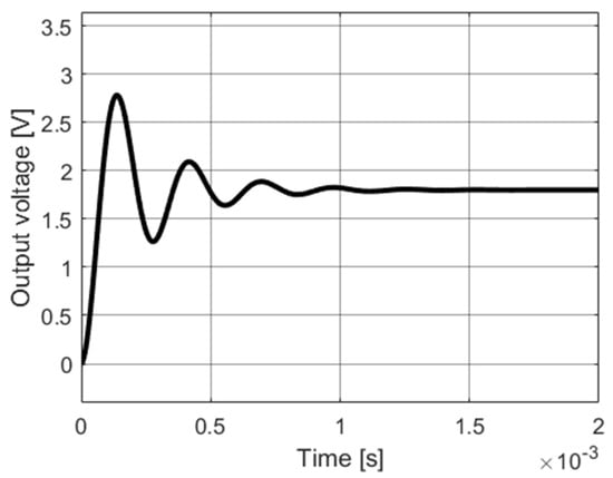
Figure 25.
Output voltage when using network 2, taking into account dead time of 100 ns.
This suggests that this analysis is correct. Neglecting the dead time during data acquisition for neural network training affects its performance in a real system, where applying the dead time is essential.
Neural Network 3
The proposed solution for this network is as follows. Since neural network 2 was trained without taking dead time into account, it is not strictly necessary to repeat the parametric simulation to generate new training data, as such a process is very time-consuming and may take several days or even weeks.
For this reason, it is possible to modify the neural network program to compensate for the dead time and thus ensure the required output voltage. Since the dead time corresponds to nine clock cycles, the CMPA value must be increased by 4.5 because the ePWM peripheral is set in UP–DOWN mode. This means that a constant can simply be added to the value calculated by neural network 2. For instance, if network 2 computes a CMPA value of 49.9, the corrected value to be written would be 54.4. The steady-state output voltage waveform for this solution is shown in Figure 26.
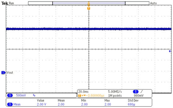
Figure 26.
Steady-state output voltage waveform when using neural network 3 under nominal conditions.
As can be seen, the steady-state value of the output voltage was also 2 V in this case. Adding a constant of 4.5 to the value calculated by neural network 2 ensured an extension of the turn-on time of the upper transistor to approximately 1.1 µs, which is shown in Figure 27.
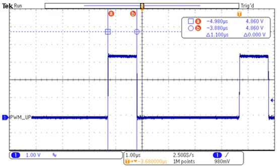
Figure 27.
Turn-on time of upper transistor when using neural network 3.
5. Neural Network 3’s Capability to Compensate for Disturbances in a Real Sample
One of the simplest ways to test the neural network’s response to parameter changes and evaluate its behavior is by adjusting the reference voltage. Figure 28 illustrates the output voltage during a reference change from 2 V to 3 V. The overshoot was minimal, and the settling time was approximately 640 µs.
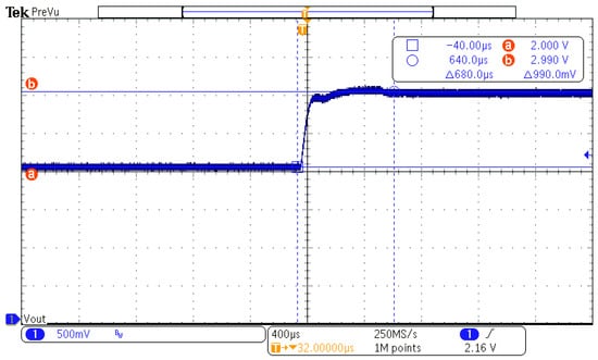
Figure 28.
Output voltage response to a change in reference from 2 V to 3 V.
The ability of the neural network to compensate for changes in the input voltage was also tested. However, this voltage can only be varied within a limited range. The maximum input voltage of the buck converter, as specified by the manufacturer, is 12 V, making testing at higher values impossible. A similar limitation applies to the lower end of the range, as the transistor driver used herein required a minimum input voltage of 8 V. Therefore, the analysis was carried out only within this interval.
Figure 29 shows the input voltage and output voltage waveforms, where the blue curve represents the output voltage and the pink curve represents the input voltage. In this measurement, the input voltage was changed from 9 V to 11 V. After the change, the output voltage stabilized at the same value as before (2.01 V) with an overshoot of approximately 70 mV. Subsequently, the input voltage was changed from 11 V to 8 V, as shown in Figure 30. In this case, the output voltage stabilized at 2.02 V, with an overshoot of about 50 mV.
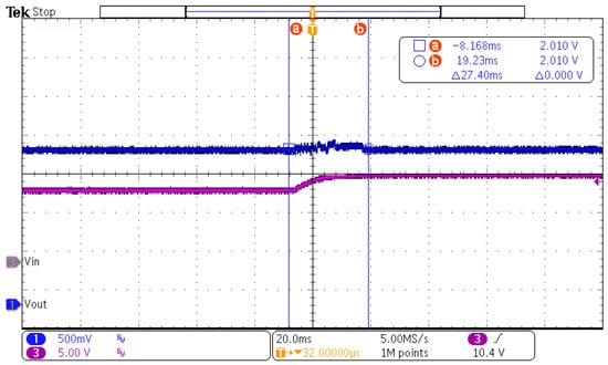
Figure 29.
Response of the output voltage to an input voltage step from 9 V to 11 V.
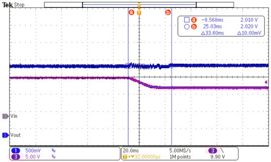
Figure 30.
Response of the output voltage to an input voltage step from 11 V to 8 V.
Subsequently, the ability of the neural network to maintain the desired output voltage value during changes in load resistance was tested. In the following figures, the output voltage waveform is shown in blue, while the output current is shown in green.
Figure 31 illustrates the case where the load changed from 7.5 Ω to 15 Ω. As shown, the output voltage stabilized at 2.01 V after this change.
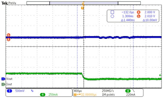
Figure 31.
Response of the output voltage to a load resistance step from 7.5 Ω to 15 Ω.
Then the resistance was changed from 7.5 Ω to 2 Ω (Figure 32). In this case, the output voltage stabilized at 2 V, although with a significantly larger overshot of approximately 150 mV.
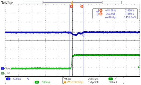
Figure 32.
Response of the output voltage to a load resistance step from 7.5 Ω to 2 Ω.
At lower load resistance values, the neural network was unable to maintain the desired voltage. Figure 33 shows a change from 7.5 Ω to 1.3 Ω, and Figure 34 shows a change from 7.5 Ω to 0.8 Ω. In both cases, the output voltage stabilized at approximately 1.92 V, which represents a relatively significant deviation from the target value of 2 V. Table 1 provides a summary of the steady-state values of the output voltage obtained from the performed measurements.
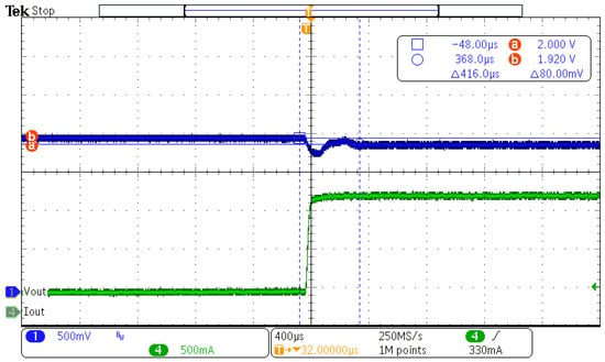
Figure 33.
Response of the output voltage to a load resistance step from 7.5 Ω to 1.3 Ω.
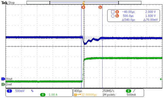
Figure 34.
Response of the output voltage to a load resistance step from 7.5 Ω to 0.8 Ω.

Table 1.
Overview of steady-state output voltage values under various parameters.
6. Conclusions
The conducted analysis confirmed that a neural network can effectively replace a traditional PID controller in the control structure of a DC/DC buck synchronous converter. Initial experiments revealed that training the network solely based on the converter’s transfer characteristic is not an ideal approach, as this method does not capture all operating states of the system. As a result, the network was capable of compensating for input voltage variations but remained unresponsive to changes in load conditions. To address this limitation, an additional input parameter was required. Specifically, the output current of the converter was introduced as the next input to the network. With this enhancement, simulation results showed that the neural network was able to successfully compensate for disturbances caused by both input voltage fluctuations and load resistance changes.
However, practical measurements showed that dead time, an essential requirement in the real-world operation of a synchronous buck converter, is often overlooked in simulations, where the system functions ideally without it. A detailed mathematical analysis, based on the behavior of the ePWM peripheral in the microprocessor used, confirmed that dead time introduces a significant deviation between the actual output voltage and the reference value. To address this deviation, a solution was proposed that avoids the need for time-consuming retraining of the neural network. Instead, a fixed offset can be added to the CMPA register value calculated by the network, compensating for the number of clock cycles lost to dead time. This modification proved effective in practice, enabling the system to deliver the correct output voltage under both nominal conditions and varying input voltage levels.
Certain limitations became apparent under varying load conditions. Specifically, at lower load resistance values, the deviation from the reference voltage increased noticeably, by several tens of millivolts, despite simulation results indicating acceptable performance at these levels. This raises the question of what contributes to this increased deviation. One possible approach to address this issue is to acquire improved training data and subsequently redesign the neural network, either by modifying its input parameters or by adjusting its architecture, such as the number of neurons or input parameters.
Author Contributions
Conceptualization, J.Š. and M.P.; methodology, J.Š.; software, J.Š. and P.K.; validation, S.K., P.K., and R.K.; formal analysis, R.K.; investigation, J.Š.; resources, S.K.; data curation, J.Š.; writing—original draft preparation, J.Š.; writing—review and editing, M.P. and R.K.; visualization, J.Š.; supervision, M.P.; project administration, P.K.; funding acquisition, M.P. All authors have read and agreed to the published version of the manuscript.
Funding
This research was funded by APVV-22-0330 “Research of a system for active and optimal management of electrical energy using battery storage system” and Vega 1/0314/24 “Research of a system for active management of electrical energy using battery storage system.”
Data Availability Statement
The data presented in this study are available in the article.
Conflicts of Interest
The authors declare no conflicts of interest.
Abbreviations
The following abbreviations are used in this manuscript:
| PID | Proportional–Integral–Derivative |
| ReLU | Rectified Linear Unit |
| ePWM | Enhanced Pulse Width Modulation |
| TBPRD | Time-Base Period Register |
| TBCLK | Time-Base Clock |
| CMPA | Compare A Register |
| HRePWM | High-Resolution Enhanced Pulse Width Modulation |
| TBCTR | Time-Base Counter Register |
References
- Das Gangula, S.; Nizami, T.K.; Udumula, R.R.; Chakravarty, A.; Singh, P. Adaptive neural network control of DC-DC power converter. Expert Syst. Appl. 2023, 229, 120362. [Google Scholar] [CrossRef]
- Pan, N.; Wu, G.; Li, R. Application of RBF neural network PID control on buck DC-DC converter. J. Phys. 2024, 2918, 012019. [Google Scholar] [CrossRef]
- Banerjee, S.; Chandwani, A.; Mallik, A. Artificial Neural Network based Direct Inverse Control for a Novel 48V-1V DC/DC Converter. In Proceedings of the 2020 IEEE International Conference on Power Electronics, Drives and Energy Systems (PEDES), Jaipur, India, 16–19 December 2020. [Google Scholar] [CrossRef]
- Muhammad, A.; Amin, A.; Qureshi, M.A.; Bhatti, A.R.; Ali, M.M. Deep learnin based buck-boost converter for PV modules. Heliyon 2024, 10, e27405. [Google Scholar] [CrossRef] [PubMed]
- Utomo, W.M.; Yi, S.S.; Buswig, Y.M.; Abu Bakar, A.; Ahmad, Z. Voltage Tracking of a DC-DC Flyback Converter Using Neural Network Control. Int. J. Power Electron. Drive Syst. 2012, 2, 35–42. [Google Scholar] [CrossRef]
- Gaied, H.; Aymen, F.; Kraiem, H.; El-Bayeh, C.Z.; Said, Y.; Almalki, M.M. Three phase bidirectional DC-DC converters based neural network controller for renewable energy sources. Front. Energy Res. 2024, 12, 1391310. [Google Scholar] [CrossRef]
- Dong, W.; Li, S.; Fu, X.; Li, Z.; Fairbank, M.; Gao, Y. Control of a Buck DC/DC Converter Using Approximate Dynamic Programming and Artificial Neural Networks. IEEE Trans. Circuits Syst. I Regul. Pap. 2021, 68, 1760–1768. [Google Scholar] [CrossRef]
- Rahman, A.U.; Mahar, M.A.; Larik, A.S. Neural Network Control of Switch Mode Dc Dc Converter. Int. J. Mod. Res. Eng. Manag. 2019, 2, 1–12. [Google Scholar]
- Saadatmand, S.; Shamsi, P.; Ferdowsi, M. The Voltage Regulation of a Buck Converter Using a Neural Network Predictive Controller. In Proceedings of the 2020 IEEE Texas Power and Energy Conference (TPCE), College Station, TX, USA, 6–7 February 2020. [Google Scholar] [CrossRef]
- Ramesh, P.; Roseline, J.F. Neural Network Based Solar-Wind Energy Using Buck Boost-Sepic Converter. Glob. J. Pure Appl. Math. 2016, 12, 1273–1281. [Google Scholar]
- Khan, H.S.; Mohamed, I.S.; Kauhaniemi, K.; Liu, L. Artificial Neural Network-Based Voltage Control of DC/DC Converter for DC Microgrid Applications. In Proceedings of the 6th IEEE Workshop on the Electronic Grid (eGRID), New Orleans, LA, USA, 8–10 November 2021. [Google Scholar] [CrossRef]
- Quan, N.V.; Son, N.N. Control of a DC-DC buck converter using adaptive neural network. Electr. Eng. 2024, 107, 6815–6825. [Google Scholar] [CrossRef]
- Liu, Z.; Yu, W. Design and Implementation of DC-DC Buck Converter based on Deep Neural Sliding Mode Control. Electr. Eng. Syst. Sci. 2024, arXiv:2405.15493. [Google Scholar] [CrossRef]
- Bote-Vazquez, M.Y.; Ramirez-Hernandez, J.; Hernandez-Gonzalez, L.; Delgado-Piña, E.D.; Juarez-Sandoval, O.U. Artificial Neural Network-Based Voltage Control in a DC-DC Converter using a Predictive Model. In Proceedings of the 2022 IEEE International Autumn Meeting on Power, Electronics and Computing (ROPEC), Ixtapa, Mexico, 9–11 November 2022. [Google Scholar] [CrossRef]
- Zilkova, J.; Timko, J.; Girovsky, P. Modeling and control of tinning line entry section using neural networks. Int. J. Simul. Model. 2012, 11, 97–109. [Google Scholar] [CrossRef]
- Girovsky, P.; Timko, J.; Zilkova, J.; Fedak, V. Neural estimators for shaft sensorless FOC control of induction motor. In Proceedings of the 14th International Power Electronics and Motion Control Conference EPE-PEMC, Ohrid, Macedonia, 6–8 September 2010. [Google Scholar] [CrossRef]
- What Is a Recurrent Neural Network? Available online: https://www.ibm.com/topics/recurrent-neural-networks (accessed on 4 October 2024).
- The Basics of Modular Neural Networks. Available online: https://www.analyticssteps.com/blogs/basics-modular-neural-networks (accessed on 15 September 2021).
- Nielsen, M.A. Neural Networks and Deep Learning; Determination Press: San Francisco, CA, USA, 2015. [Google Scholar]
- Rojas, R. Neural Networks: A Systematic Introduction; Springer: Berlin/Heidelberg, Germany, 1996. [Google Scholar]
- Goodfellow, I.; Bengio, Y.; Courville, A. Deep Learning; MIT Press: Cambridge, MA, USA, 2016. [Google Scholar]


Disclaimer/Publisher’s Note: The statements, opinions and data contained in all publications are solely those of the individual author(s) and contributor(s) and not of MDPI and/or the editor(s). MDPI and/or the editor(s) disclaim responsibility for any injury to people or property resulting from any ideas, methods, instructions or products referred to in the content. |
© 2025 by the authors. Licensee MDPI, Basel, Switzerland. This article is an open access article distributed under the terms and conditions of the Creative Commons Attribution (CC BY) license (https://creativecommons.org/licenses/by/4.0/).