
Analysis and Parameter Design of SiC-Based Current Source Inverter (CSI)


Abstract
:1. Introduction
2. Operation and Modeling of CSIs
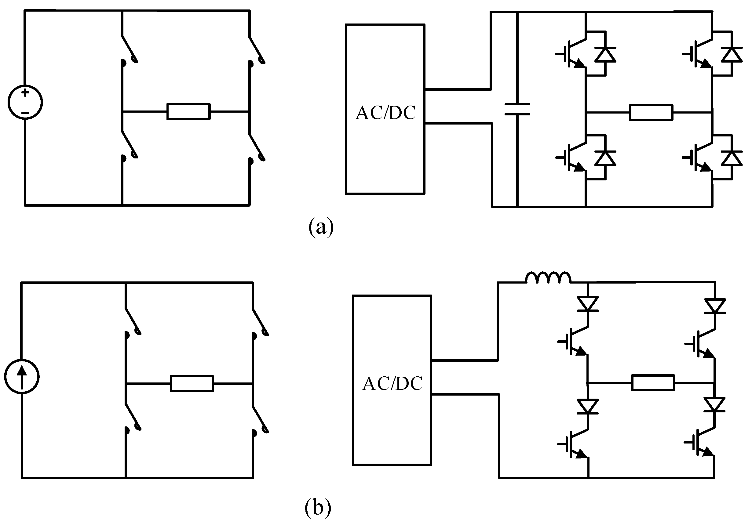
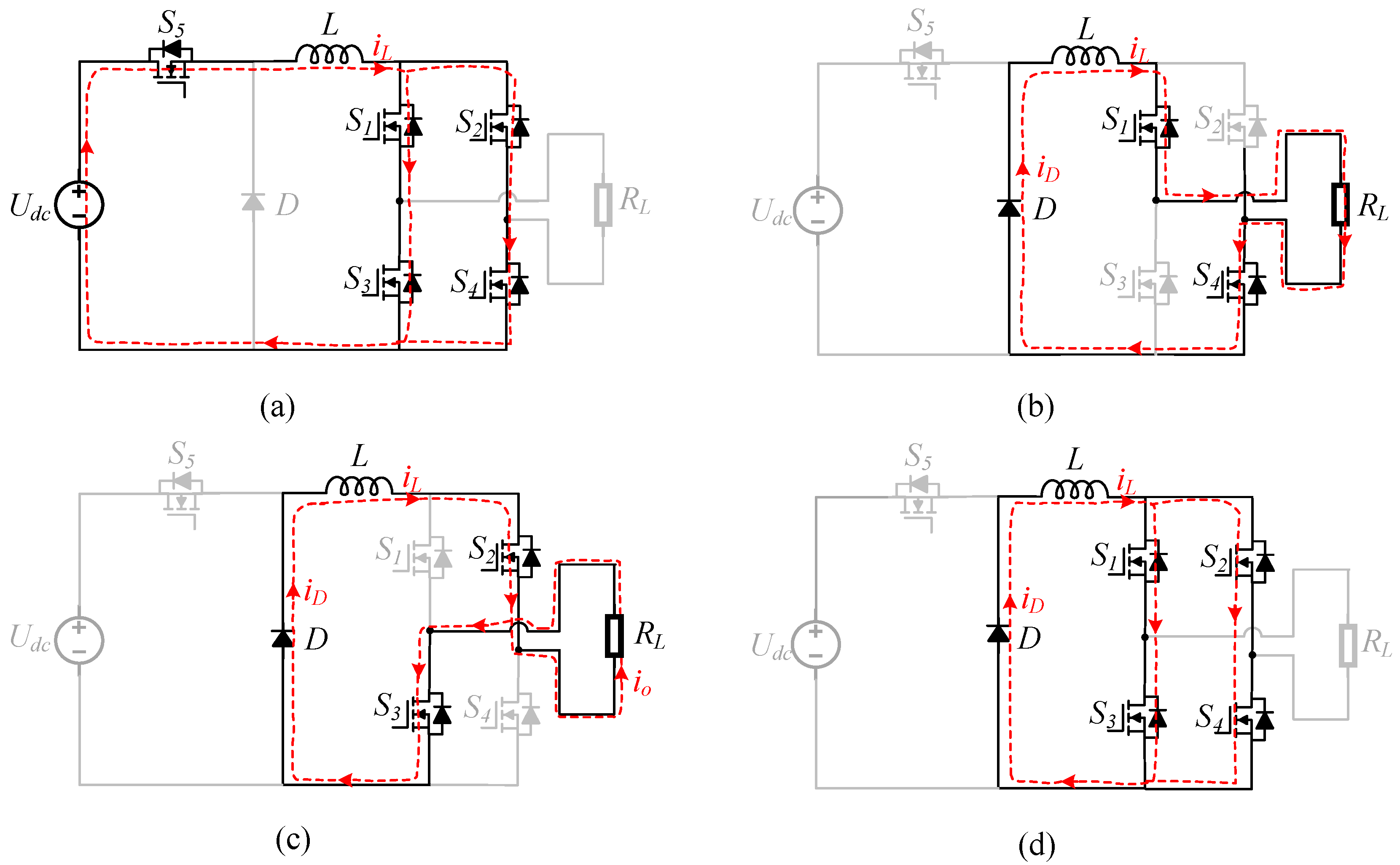
2.1. Circuits, Operation Principles, and Modulation Scheme
2.2. Operation Principles and Two Models
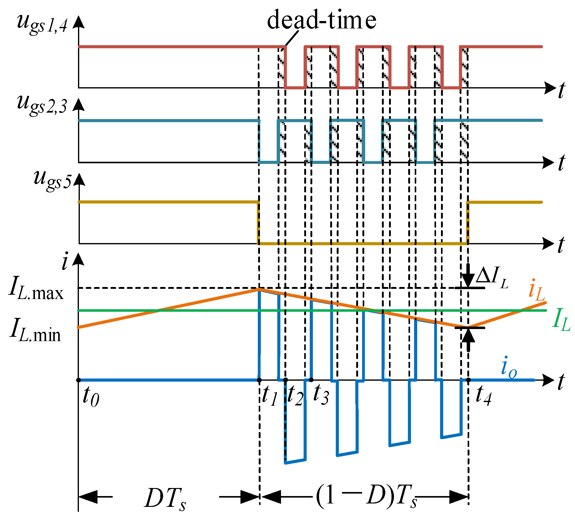
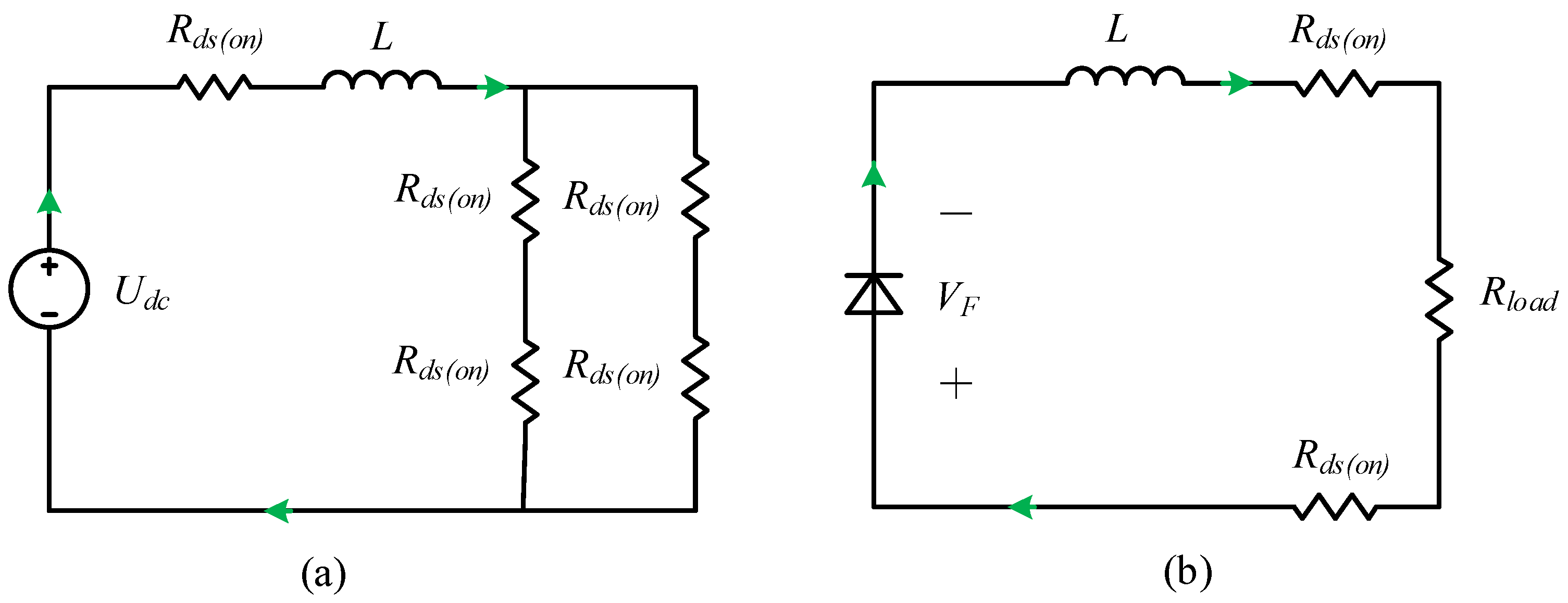
2.2.1. Simplified Model
- (1)
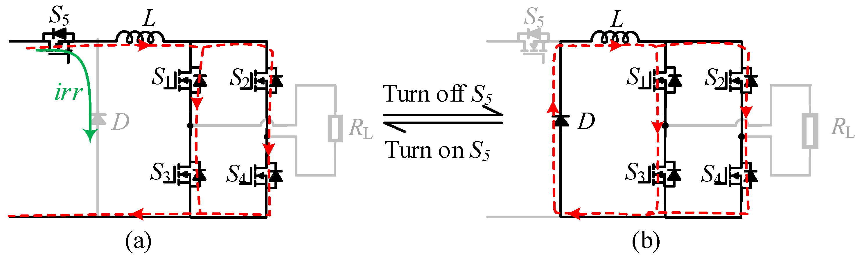
- The charging stage: (t0 − t1)
- (2)
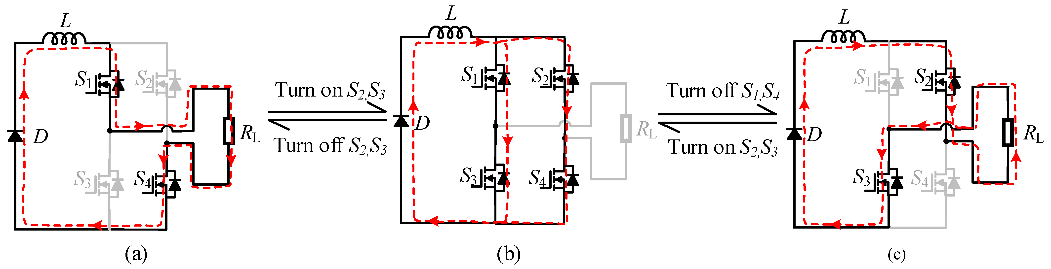
- The discharging stage: (t1–t4)
2.2.2. Precise Model
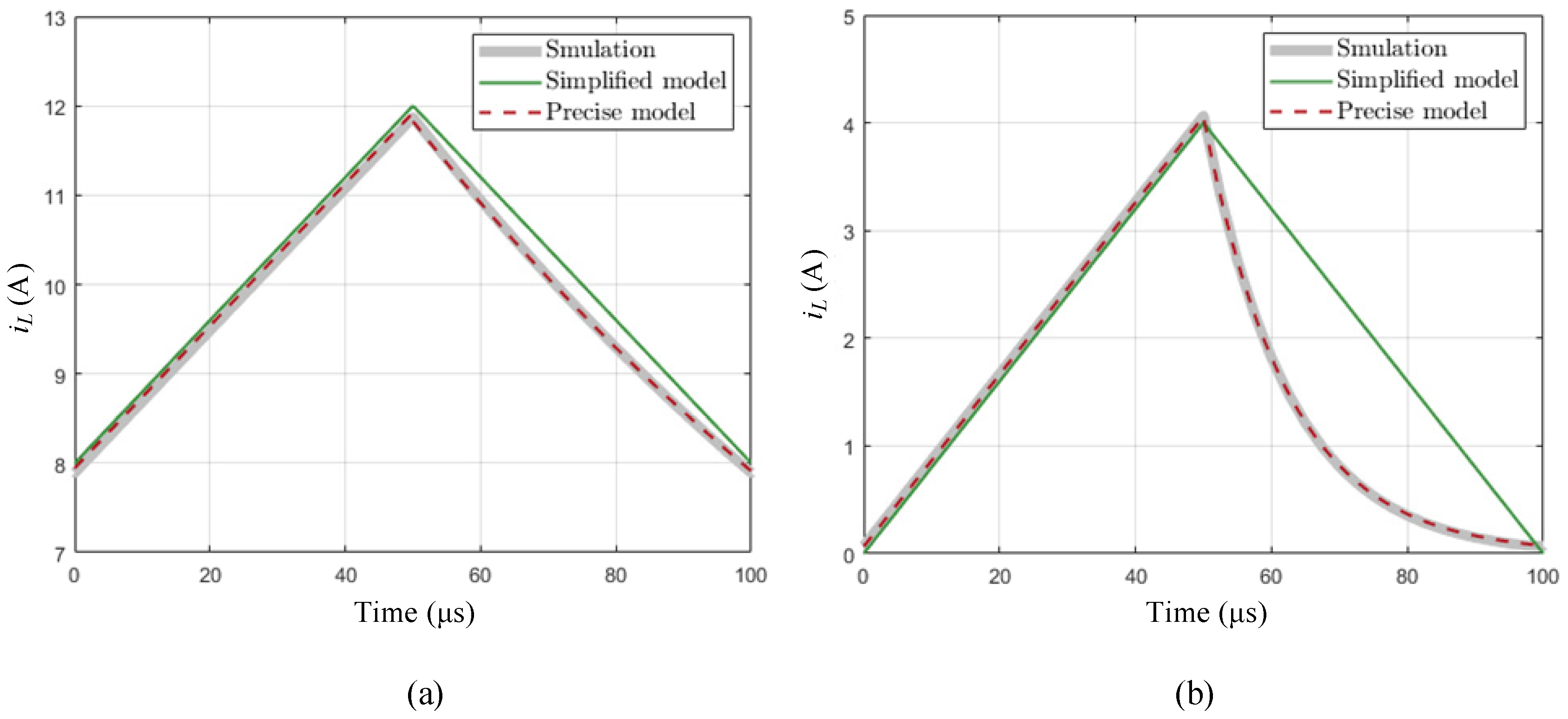
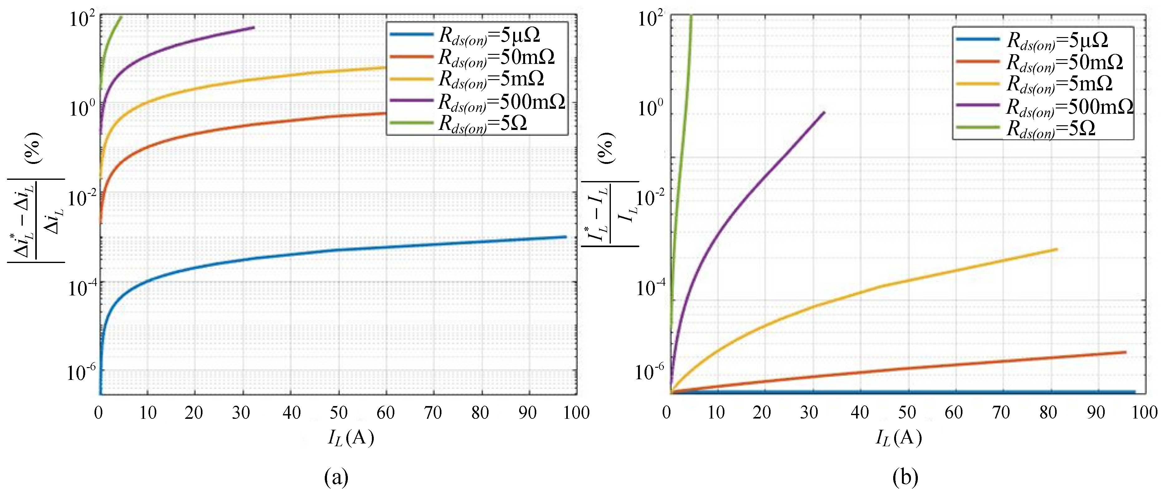
2.3. Model Comparison and Error Analysis
2.4. Parameter Design Based on Simplified Model
2.4.1. Inductor Design
Inverter Working in CCM Mode
The Current Ripple
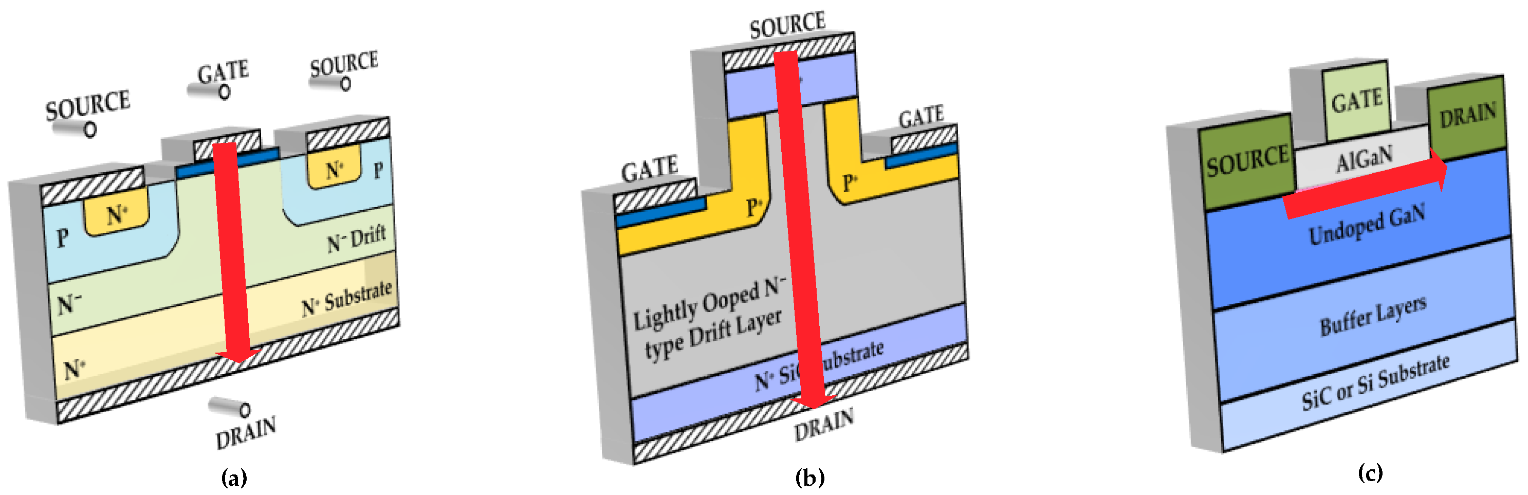
2.4.2. Active Switches Selection
Voltage Stress
Current Capability of Switches
2.4.3. Freewheeling Diode Selection
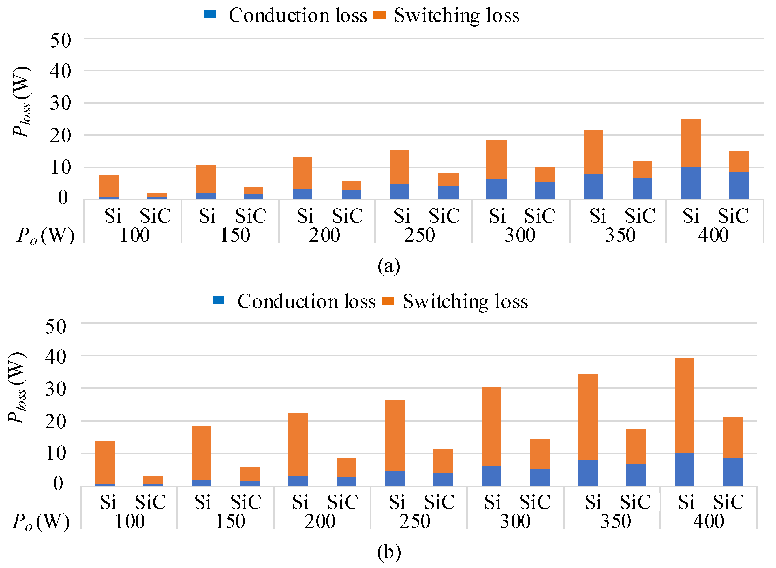
3. Power Loss Estimation Based on the Precise Model
3.1. Conduction Loss
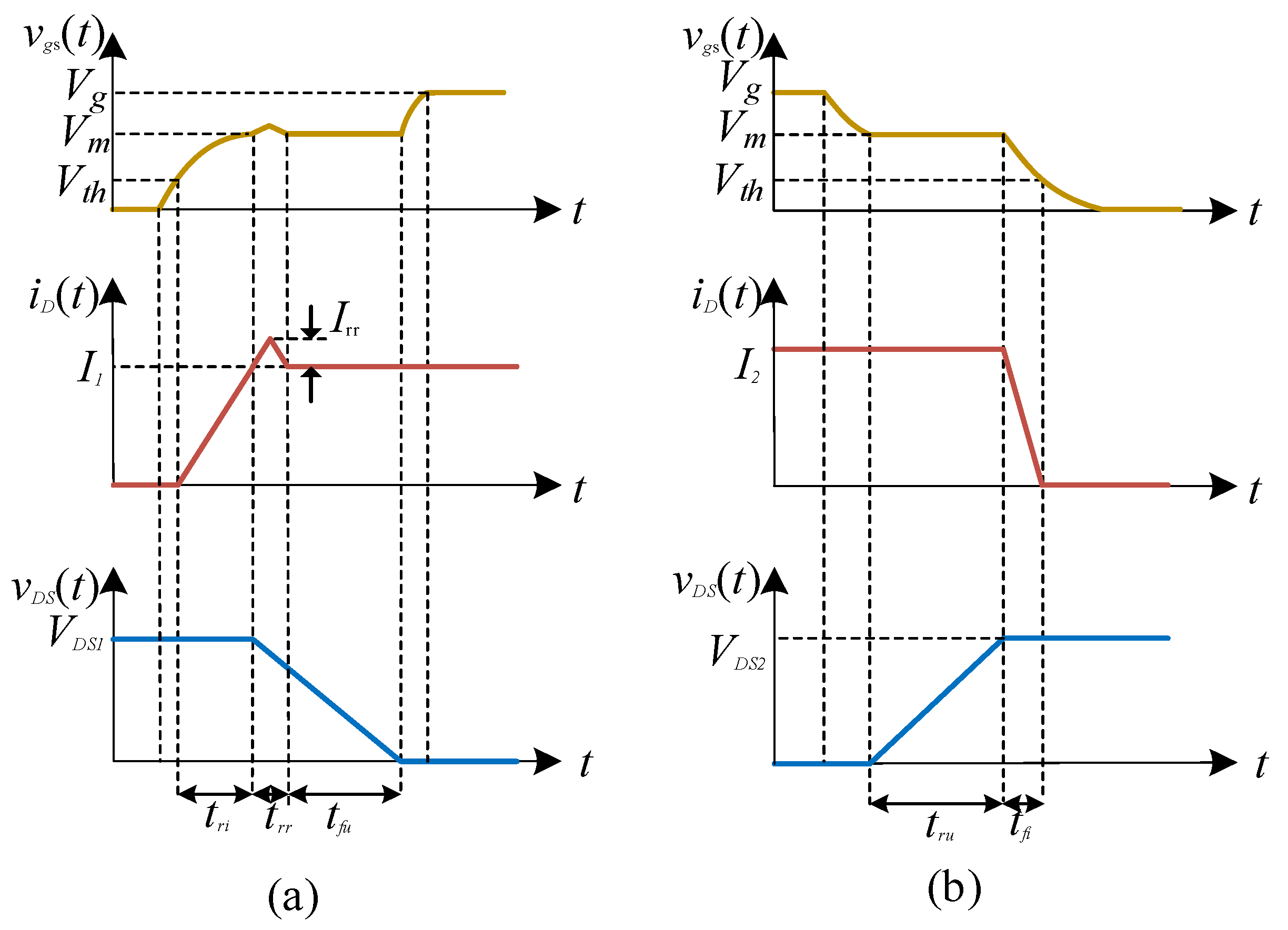
3.2. Switching Loss
- (a)
- Analysis of Communication between the Charging and Discharging States
- (b)
- Analysis of Communication between the P- and N-Modes during the Discharging State
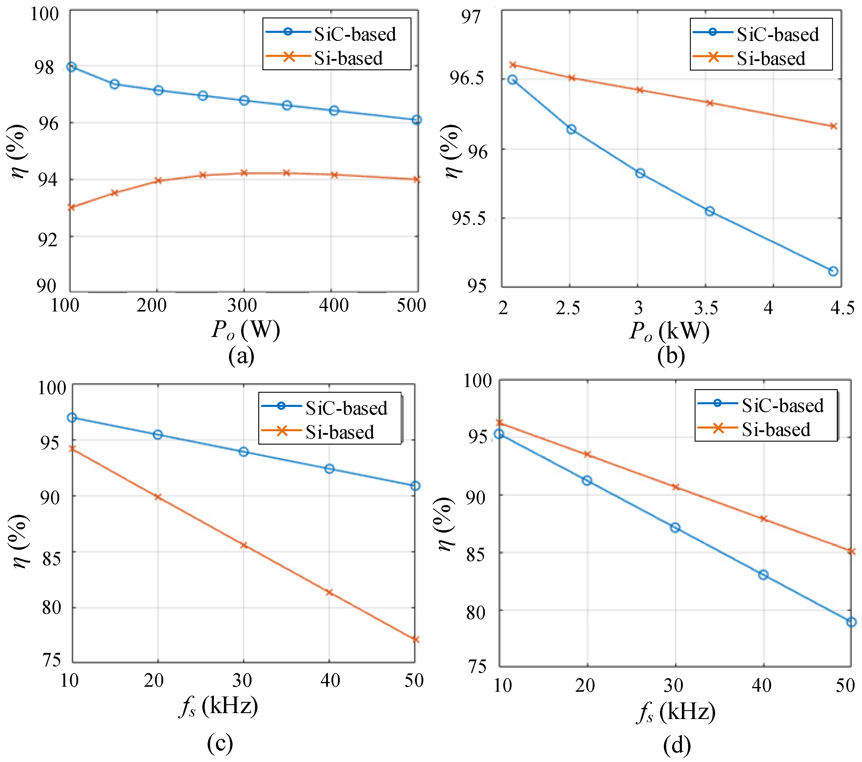
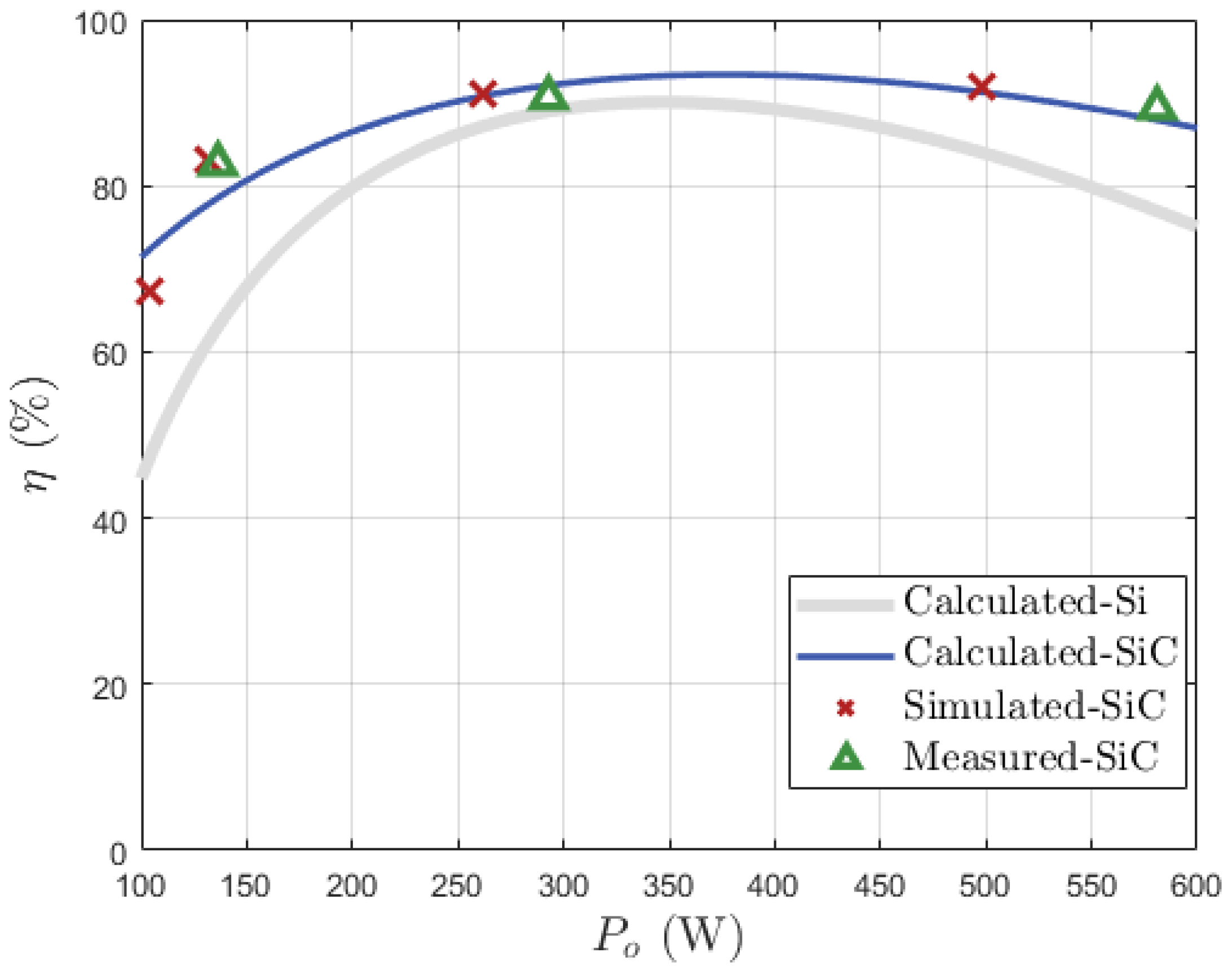
3.3. Efficiency Comparison between Si- and SiC-Based CSIs
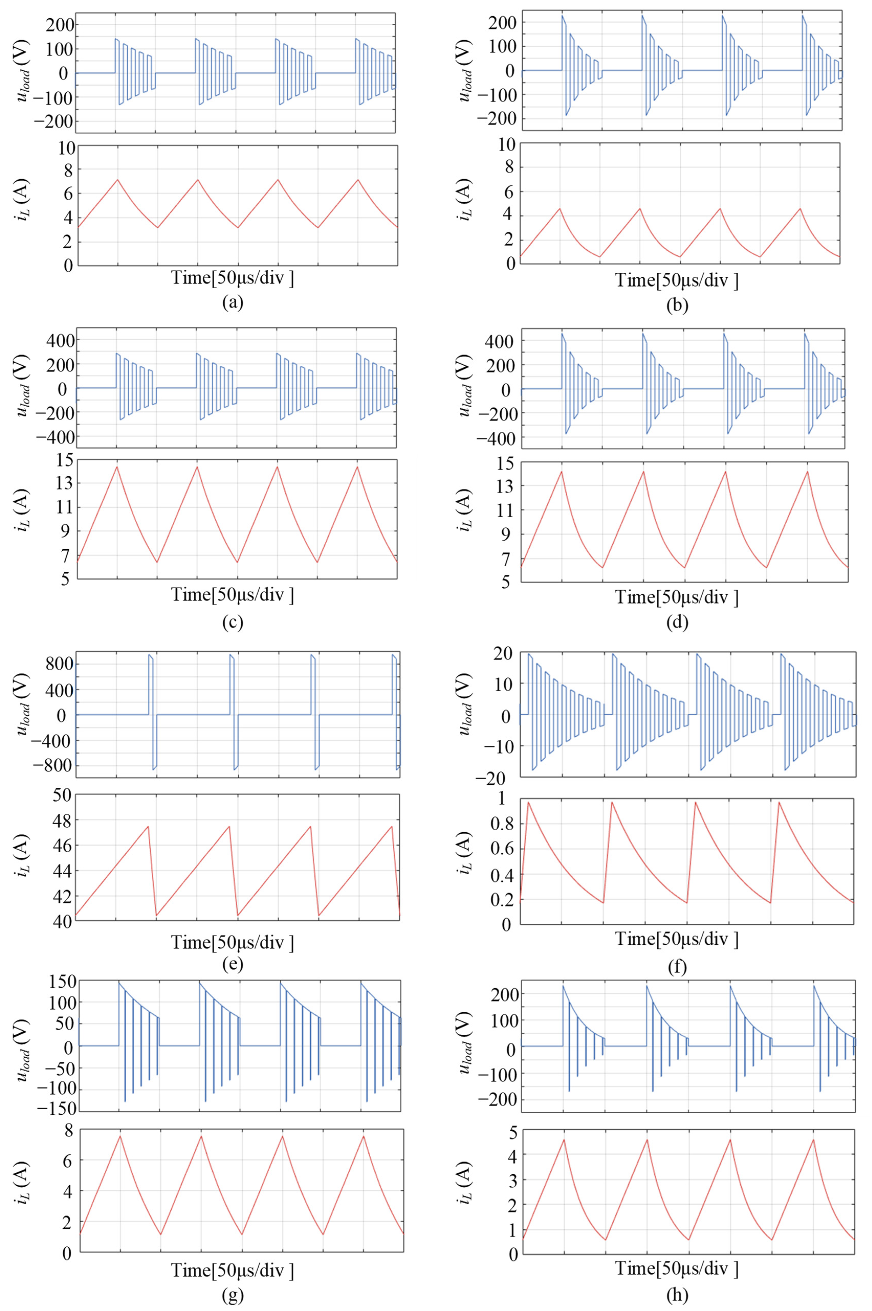
4. Simulation and Experimental Verification
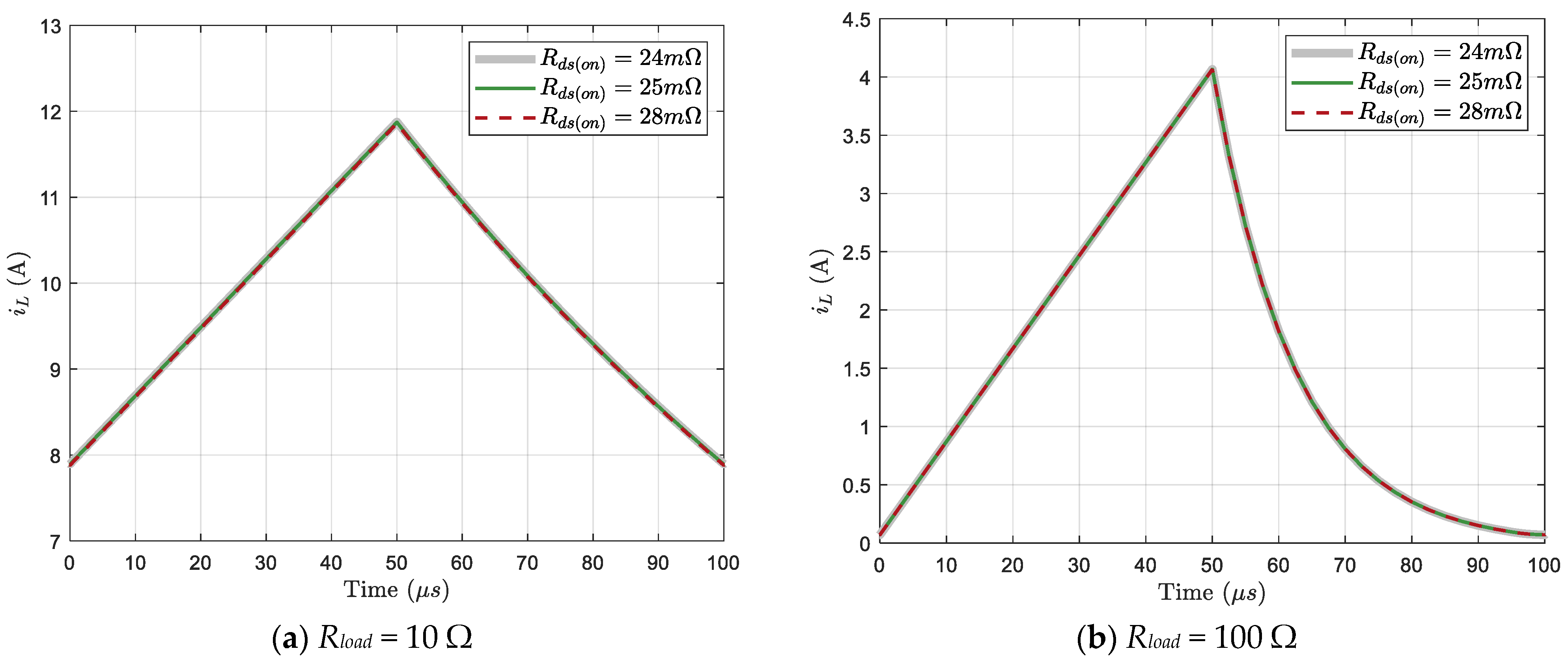
4.1. Simulation Results
4.2. Experiments Results
5. Conclusions
Author Contributions
Funding
Data Availability Statement
Acknowledgments
Conflicts of Interest
References
- Zhao, H.; Shen, Y.; Ying, W.; Ghosh, S.S.; Ahmed, M.R.; Long, T. A single-and three-phase grid compatible converter for electric vehicle on-board chargers. IEEE Trans. Power Electron. 2019, 35, 7545–7562. [Google Scholar] [CrossRef]
- Kwon, M.; Choi, S. An electrolytic capacitorless bidirectional EV charger for V2G and V2H applications. IEEE Trans. Power Electron. 2016, 32, 6792–6799. [Google Scholar] [CrossRef]
- De Bernardinis, A.; Kolli, A.; Ousten, J.; Lallemand, R. High efficiency Silicon carbide DC-AC inverter for EV-charging Flywheel system. In Proceedings of the 2017 IEEE Transportation Electrification Conference and Expo (ITEC), Chicago, IL, USA, 22–24 June 2017. [Google Scholar]
- Xiao, Y.; Liu, C.; Yu, F. An integrated on-board EV charger with safe charging operation for three-phase IPM motor. IEEE Trans. Ind. Electron. 2018, 66, 7551–7560. [Google Scholar] [CrossRef]
- Wang, X.; Jiang, C.; Lei, B.; Teng, H.; Bai, H.K.; Kirtley, J.L. Power-loss analysis and efficiency maximization of a silicon-carbide MOSFET-based three-phase 10-kW bidirectional EV charger using variable-DC-bus control. IEEE J. Emerg. Sel. Topics Power Electron. 2016, 4, 880–892. [Google Scholar] [CrossRef]
- Sujitha, N.; Krithiga, S. RES based EV battery charging system: A review. Renew. Sustain. Energy Rev. 2017, 75, 978–988. [Google Scholar] [CrossRef]
- Schöner, C.; Derix, D.; Hensel, A. Comparison and evaluation of different three-level inverter topologies for PV systems. In Proceedings of the 2014 16th European Conference on Power Electronics and Applications, Lappeenranta, Finland, 26–28 August 2014. [Google Scholar]
- Traube, J.; Lu, F.; Maksimovic, D.; Mossoba, J.; Kromer, M.; Faill, P.; Katz, S.; Borowy, B.; Nichols, S.; Casey, L. Mitigation of solar irradiance intermittency in photovoltaic power systems with integrated electric-vehicle charging functionality. IEEE Trans. Power Electron. 2012, 28, 3058–3067. [Google Scholar] [CrossRef]
- Burger, B.; Kranzer, D.; Stalter, O. Cost reduction of PV-inverters with SiC-DMOSFETs. In Proceedings of the 5th International Conference on Integrated Power Electronics Systems, Nuremberg, Germany, 11–13 March 2008. [Google Scholar]
- Rajalakshmi, S.; Rangarajan, P. Investigation of modified multilevel inverter topology for PV system. Microprocess. Microsy. 2019, 71, 102870. [Google Scholar] [CrossRef]
- Weckx, S.; Driesen, J. Load balancing with EV chargers and PV inverters in unbalanced distribution grids. IEEE Trans. Sustain. Energy 2015, 6, 635–643. [Google Scholar] [CrossRef] [Green Version]
- Baiju, M.R.; Mohapatra, K.K.; Kanchan, R.S.; Gopakumar, K. A dual two-level inverter scheme with common mode voltage elimination for an induction motor drive. IEEE Trans. Power Electron. 2004, 19, 794–805. [Google Scholar] [CrossRef] [Green Version]
- Wang, F. Motor shaft voltages and bearing currents and their reduction in multilevel medium-voltage PWM voltage-source-inverter drive applications. IEEE Trans. Ind. Appl. 2000, 36, 1336–1341. [Google Scholar] [CrossRef]
- Ye, Z.; Lei, Y.; Pilawa-Podgurski, R.C. A 48-to-12 V cascaded resonant switched-capacitor converter for data centers with 99% peak efficiency and 2500 W/in 3 power density. In Proceedings of the 2019 IEEE Applied Power Electronics Conference and Exposition (APEC), Anaheim, CA, USA, 17–21 March 2019. [Google Scholar]
- Saggini, S.; Jiang, S.; Ursino, M.; Nan, C. A 99% efficient dual-phase resonant switched-capacitor-buck converter for 48 v data center bus conversions. In Proceedings of the 2019 IEEE Applied Power Electronics Conference and Exposition (APEC), Anaheim, CA, USA, 17–21 March 2019. [Google Scholar]
- Simanjorang, R.; Yamaguchi, H.; Ohashi, H.; Nakao, K.; Ninomiya, T.; Abe, S.; Kaga, M.; Fukui, A. High-efficiency high-power dc-dc converter for energy and space saving of power-supply system in a data center. In Proceedings of the 2011 Twenty-Sixth Annual IEEE Applied Power Electronics Conference and Exposition (APEC), Worth, TX, USA, 6–11 March 2011. [Google Scholar]
- Ahmed, M.H.; Lee, F.C.; Li, Q. Two-stage 48-V VRM with intermediate bus voltage optimization for data centers. IEEE J. Emerg. Sel. Topics Power Electron. 2020, 9, 702–715. [Google Scholar] [CrossRef]
- Lai, C.; Teh, J.; Cheng, Y.; Li, Y. A reflex-charging based bidirectional DC charger for light electric vehicle and DC-microgrids. In Proceedings of the TENCON 2017-2017 IEEE Region 10 Conference, Penang, Malaysia, 5–8 November 2017. [Google Scholar]
- Coelho, S.; Monteiro, V.; Sousa, T.J.C.; Barros, L.A.M.; Pedrosa, D.; Couto, C.; Afonso, J.L. A Unified Power Converter for Solar PV and Energy Storage in dc Microgrids. Batteries 2022, 8, 143. [Google Scholar] [CrossRef]
- Ma, C.-T. System Planning of Grid-Connected Electric Vehicle Charging Stations and Key Technologies: A Review. Energies 2019, 12, 4201. [Google Scholar] [CrossRef] [Green Version]
- Hua, C.; Lin, M. A study of charging control of lead-acid battery for electric vehicles. In Proceedings of the 2000 IEEE International Symposium on Industrial Electronics (Cat. No. 00TH8543), Cholula, Mexico, 4–8 December 2000; pp. 135–140. [Google Scholar]
- Chen, L.; Chu, N.; Wang, C.; Liang, R. Design of a reflex-based bidirectional converter with the energy recovery function. IEEE Trans. Ind. Electron. 2008, 55, 3022–3029. [Google Scholar] [CrossRef]
- Liang, T.; Wen, T.; Tseng, K.C.; Chen, J. Implementation of a regenerative pulse charger using hybrid buck-boost converter. In Proceedings of the 4th IEEE International Conference on Power Electronics and Drive Systems, IEEE PEDS 2001-Indonesia. Proceedings (Cat. No. 01TH8594), Denpasar, Indonesia, 22–25 October 2001; pp. 437–442. [Google Scholar]
- Xu, J.; Yang, X.; Zhao, H.; Qiu, J.; Liu, K. An Inductor-Based and Capacitor-Free Bipolar Pulse Converter with Overvoltage Protection. World Electr. Veh. J. 2022, 13, 91. [Google Scholar] [CrossRef]
- Yifeng, G.; Chengning, Z. Study on the fast charging method of lead-acid battery with negative pulse discharge. In Proceedings of the 2011 4th International Conference on Power Electronics Systems and Applications, Hongkong, China, 8–10 June 2011. [Google Scholar]
- Marcos, J.; Dios, J.; Cao, A.M.; Doval, J.; Penalver, C.M.; Nogueiras, A.; Lago, A.; Poza, F. Fast lead-acid battery charge strategy. In Proceedings of the Twenty-First Annual IEEE Applied Power Electronics Conference and Exposition, Dallas, TX, USA, 19–23 March 2006. [Google Scholar]
- Tsai, C.; Kuo, Y.; Kuo, Y.; Hsieh, C. A reflex charger with ZVS and non-dissipative cells for photovoltaic energy conversion. Energies 2015, 8, 1373–1389. [Google Scholar] [CrossRef]
- Luo, F.L.; Ye, H. Advanced dc/dc Converters; CRC Press: Boca Raton, FL, USA, 2016; ISBN 1315393786. [Google Scholar]
- Ledwich, G. Current source inverter modulation. IEEE Trans. Power Electron. 1991, 6, 618–623. [Google Scholar] [CrossRef]
- Séguier, G.; Labrique, F. Power Electronic Converters: DC-AC Conversion; Springer Science & Business Media: Berlin/Heidelberg, Germany, 2012; ISBN 3642503225. [Google Scholar]
- Luo, F.L.; Ye, H. Power Electronics: Advanced Conversion Technologies; CRC Press: Boca Raton, FL, USA, 2018; ISBN 1315186276. [Google Scholar]
- Wang, H.; Yang, X.; Madeniyeti, N.; Qiu, J.; Zhu, C.; Yin, L.; Liu, K. Temperature distribution of vessel tissue by high frequency electric welding with combination optical measure and simulation. Biosensors 2022, 12, 209. [Google Scholar] [CrossRef] [PubMed]
- Yin, L.; Zhu, C.; Xu, J.; Zhao, H.; Qiu, J.; Wang, H.; Liu, K. Dynamic Impedance Analysis of Intestinal Anastomosis during High-Frequency Electric Field Welding Process. Sensors 2022, 22, 4101. [Google Scholar] [CrossRef] [PubMed]
- Wang, H.; Blaabjerg, F. Reliability of capacitors for DC-link applications in power electronic converters—An overview. IEEE Trans. Ind. Appl. 2014, 50, 3569–3578. [Google Scholar] [CrossRef]
- Friedrichs, D.A.; Erickson, R.W.; Gilbert, J. A new dual current-mode controller improves power regulation in electrosurgical generators. IEEE Trans. Biomed. Circuits Syst. 2011, 6, 39–44. [Google Scholar] [CrossRef] [PubMed]
- Zhao, J.H.; Alexandrov, P.; Li, X. Demonstration of the first 10-kV 4H-SiC Schottky barrier diodes. IEEE Electron Device Lett. 2003, 24, 402–404. [Google Scholar] [CrossRef]
- Neudeck, P.G. SiC technology. In The VLSI Handbook; Raton, B., Ed.; CRC Press: Boca Raton, FL, USA; IEEE Press: Piscataway, NJ, USA, 2000; pp. 6.1–6.24. [Google Scholar]
- Carter, C.H., Jr.; Tsvetkov, V.F.; Glass, R.C.; Henshall, D.; Brady, M.; Müller, S.G.; Kordina, O.; Irvine, K.; Edmond, J.A.; Kong, H. Progress in SiC: From material growth to commercial device development. Mater. Sci. Eng. B 1999, 61, 1–8. [Google Scholar] [CrossRef]
- Singer, S.; Erickson, R.W. Power-source element and its properties. IEEE Proc.-Circuits Devices Syst. 1994, 141, 220–226. [Google Scholar] [CrossRef]
- On Semiconductor “Wide Bandgap Solutions”. Available online: www.onsemi.com/solutions-applications/segments/industrial-cloud-power/computing-peripherals/wide-bandgap-solutions, (accessed on 10 September 2022).
- Information, S.P. Compound Semiconductors: What Are “SiC” and “GaN”? Available online: www.semicon.sanken-ele.co.jp/en/guide/GaNSiC.html (accessed on 12 September 2022).
- Bottaro, E.; Rizzo, S.A.; Salerno, N. Circuit Models of Power MOSFETs Leading the Way of GaN HEMT Modelling—A Review. Energies 2022, 15, 3415. [Google Scholar] [CrossRef]
- Garcia, J.; Saeed, S.; Gurpinar, E.; Castellazzi, A. A Study of Integrated Signal and Power Transfer for Compact Isolated SiC MOSFET Gate-Drivers. Electronics 2021, 10, 159. [Google Scholar] [CrossRef]
- Singh, R.; Cooper, J.A.; Melloch, M.R.; Chow, T.P.; Palmour, J.W. SiC power Schottky and PiN diodes. IEEE Trans. Electron Devices 2002, 49, 665–672. [Google Scholar] [CrossRef]
- Hu, J. Integration Challenges in High Power Density Wide Bandgap Based Circuits for Transportation Applications; Virginia Tech: Blacksburg, VA, USA, 2021. [Google Scholar]
- Wang, Y.; Ding, Y.; Yin, Y. Reliability of Wide Band Gap Power Electronic Semiconductor and Packaging: A Review. Energies 2022, 15, 6670. [Google Scholar] [CrossRef]
- Chaturvedi, M.; Dimitrijev, S.; Haasmann, D.; Moghadam, H.A.; Pande, P.; Jadli, U. A Figure of Merit for Selection of the Best Family of SiC Power MOSFETs. Electronics 2022, 11, 1433. [Google Scholar] [CrossRef]
- Palmer, P.; Zhang, X.; Shelton, E.; Zhang, T.; Zhang, J. An experimental comparison of GaN, SiC and Si switching power devices. In Proceedings of the IECON 2017-43rd Annual Conference of the IEEE Industrial Electronics Society, Beijing, China, 29 October–1 November 2017. [Google Scholar]
- Li, K.; Evans, P.; Johnson, M. SiC/GaN power semiconductor devices: A theoretical comparison and experimental evaluation under different switching conditions. IET Electr. Syst. Transp. 2018, 8, 3–11. [Google Scholar] [CrossRef]
- Cree, “Silicon Carbide Power MOSFET C3MTM MOSFET Technology,” C3M0025065D Datasheet Rev 1, [Revised December 2020]. Available online: https://assets.wolfspeed.com/uploads/2021/05/C3M0025065D.pdf (accessed on 10 September 2022).
- Infineon, “600V CoolMOSTM P7 Power Transistor,” IPW60R037P7 Datasheet Rev 2.3, [Revised June 2018]. Available online: www.infineon.com/dgdl/Infineon-IPW60R037P7-DS-v02_03-EN.pdf?fileId=5546d46259d9a4bf015a5bb7bab83ca7 (accessed on 10 September 2022).


| Electrical Property | Si | SiC | GaN |
|---|---|---|---|
| Band Gap Energy (eV) | 1.1 | 3.26 | 3.4 |
| Electric Field (×106 V/cm) | 0.3 | 3 | 3.5 |
| Electron Mobility (×103 cm2/V·s) | 1.3 | 0.9 | 0.9–2 |
| Thermal Conductivity (W/cm·K) | 1.5 | 3.7 | 1.3 |
| Saturation Drift Velocity (×107 cm/s) | 1.0 | 2.0 | 2.5 |
| Symbol | Parameter |
|---|---|
| L | Power Inductor |
| S1~S5 | Switches |
| UDC | Input DC Voltage |
| Rload | Load Impedance |
| IL | Average Inductor Current |
| IL.max | Inductor Current Peak Value |
| IL.min | Inductor Current Valley Value |
| ΔiL | Inductor Current Ripple |
| fs | Switching Frequency of S5 |
| Ts | Inverter Working Period |
| fsw | Switching Frequency of S1–S4 |
| D | Duty Cycle of S5 |
| Rds(on) | MOSFET On-State Resistance |
| VF | Diode Forward Voltage |
| pcon | MOSFET Conduction Loss |
| pswi | MOSFET Switching Loss |
| Eon | MOSFET Turn-On Switching Energy |
| Eoff | MOSFET Turn-Off Switching Energy |
| Eswi | MOSFET Switching Energy |
| Rds(on) @25 °C | SiC MOSFET (C3M0025065D, Vgs = 15 V) | Si MOSFET (IPW60R037P7, Vgs = 10V) |
|---|---|---|
| Minimum | 24 (ID = 10A) | 60 (ID = 0 A) |
| Typical Value | 25 (ID = 33.5A) | 37 (ID = 29.5 A) |
| Maximum | 28 (ID = 135A) | 95 (ID = 135 A) |
| Parameter | SiC MOSFET CREE C3M0025065D | Si MOSFET Infineon IPW60R037P7 |
|---|---|---|
| Vds (V) | 650 | 650 |
| d (A) | 97 | 76 |
| Id(pulse) (A) | 251 | 280 |
| Rdson (mΩ) | 25 | 37 |
| Ciss (pF) | 2980 | 5243 |
| Coss (pF) | 178 | 85 |
| Crss (pF) | 12 | 156 |
| Qg (nC) | 108 | 121 |
| trr (ns) | 51 | 300 |
| Tj,Tstg (°C) | −55~150 | −40~175 |
| Price @ quantity = 1 ($) Note 1 | 27.87 | 13.92 |
| Parameter | Value |
|---|---|
| L (mH) | 1.25 |
| Vdc (V) | 100, 200 |
| Rload (Ω) | 10, 20, 50, 100 |
| fs (kHz) | 10 |
| D | 0.1~0.9 |
| fsw (kHz) | 100 |
Publisher’s Note: MDPI stays neutral with regard to jurisdictional claims in published maps and institutional affiliations. |
© 2022 by the authors. Licensee MDPI, Basel, Switzerland. This article is an open access article distributed under the terms and conditions of the Creative Commons Attribution (CC BY) license (https://creativecommons.org/licenses/by/4.0/).
Share and Cite
Yang, X.; Zhao, Z.; Wang, C.; Xu, J.; Liu, K.; Qiu, J. Analysis and Parameter Design of SiC-Based Current Source Inverter (CSI). World Electr. Veh. J. 2022, 13, 187. https://doi.org/10.3390/wevj13100187
Yang X, Zhao Z, Wang C, Xu J, Liu K, Qiu J. Analysis and Parameter Design of SiC-Based Current Source Inverter (CSI). World Electric Vehicle Journal. 2022; 13(10):187. https://doi.org/10.3390/wevj13100187
Chicago/Turabian StyleYang, Xingjian, Zhennan Zhao, Cheng Wang, Jianzhi Xu, Kefu Liu, and Jian Qiu. 2022. "Analysis and Parameter Design of SiC-Based Current Source Inverter (CSI)" World Electric Vehicle Journal 13, no. 10: 187. https://doi.org/10.3390/wevj13100187