Abstract
For an actual visible light communication system, it is necessary to consider the uniformity of indoor illumination. Most of the existing optimization schemes, however, do not consider the effect of the first reflected light, and do not conform to the practical application conventions, which increases the actual cost and the complexity of system construction. In this paper, considering the first reflected light and based on the conventional layout model and the classic indoor visible light communication model, a scheme using the parameter Q to determine the optimal layout of channel quality is proposed. We determined the layout, and then carried out a simulation. For comparison, the normal layout and the optimal layout of illumination were also simulated. The simulation results show that the illuminance distributions of the three layouts meet the standards of the International Organization for Standardization. The optimal layout of channel quality in the signal-to-noise ratio distribution, maximum delay spread distribution, and impulse response is obviously better than the optimal layout of illumination. In particular, the effective area percentage of the optimal layout of channel quality is increased by 0.32% and 6.08% to 88.80% as compared with the normal layout’s 88.48% and the optimal layout of illumination’s 82.72%. However, compared with the normal layout, the advantages are not very prominent.
1. Introduction
For an actual visible light communication (VLC) system, it is necessary to consider the uniformity of indoor illumination, so it is preferred to use light-emitting diodes (LEDs) with a larger half-power angle, which enhances the multipath effect while causing inter-symbol interference (ISI) and reducing the signal-to-noise ratio (SNR). In order to improve the performance of a VLC system, various optimization schemes have been proposed [1,2,3,4,5].
An optimization scheme based on an evolutionary algorithm is proposed to modify the optical intensity of LED transmitters for reducing the signal power fluctuation extent [1]. A new arrangement scheme of LED lamps is proposed, and the SNR fluctuation is reduced from 14.5 to 0.9 dB [2]. A hybrid scheme that combines spotlighting with uniform lighting is proposed to achieve uniform illumination and high data rate [3]. An optimization scheme based on light-shaping diffusers is proposed to achieve uniform power distribution [4]. An optimization scheme based on the Lambertian order is proposed to improve the performance of a VLC system [5].
According to published papers [6,7], it is necessary to consider the effect of the first reflected light, but most of the existing optimization schemes only consider the direct radiation, and the optimization results usually do not conform to the practical application conventions, which increase the actual cost and the complexity of system construction. In this paper, considering the first reflected light and based on the conventional layout model and the classic indoor VLC model, the normal layout, the optimal layout of illumination, and the optimal layout are simulated, and the relevant data are analyzed.
Following the introduction, this paper is organized in four sections. In Section 2, the basic theories and calculation formulas of VLC simulation are shown. In Section 3, the data and indoor environment used in the simulation are shown, the parameter Q is defined, and the three layouts are determined. In Section 4, the illuminance distribution, SNR distribution, maximum delay spread (M-DS) distribution, and impulse response (IR) of the three layouts are shown and analyzed. Finally, our conclusions are given in Section 5.
2. Basic Theories of VLC
This section is divided into three parts, which respectively explain the basic theories and calculation formulas used in the simulation of illuminance, optical radiation power, and channel quality in VLC. In existing papers [5,6], it is assumed that the light source is a near-Lambertian light source and the reflective surface is a standard Lambertian surface. These two assumptions are used in this paper. Some basic photometric parameters are described below.
The basic physical quantity used in optical radiometry is the radiant flux or radiant power, symbolized by Φe in watts (W). Photometry is a discipline that studies the senses of human eyes. The units used are based on a physical basis and the characteristics of the human eye. Therefore, all units in photometry are artificial.
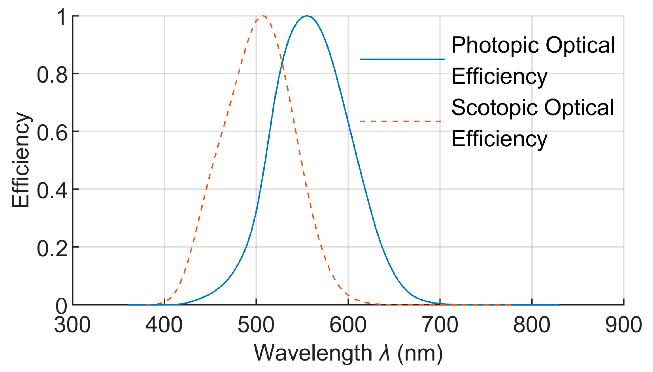
Luminous flux indicates the visual intensity of the human eye caused by radiant flux, which is the physical quantity derived from the radiant flux Φe, that is, the photometric quantity of the radiant flux, based on the effect of the radiation on the standard photometric observer of the International Commission on illumination (CIE). Luminous flux is an intrinsic property of a light source. The symbol is Φv and the unit is lumen (lm = cd·sr):
where V(λ) is the photopic optical efficiency function, as shown in Figure 1; Km is the photopic optical efficiency at λ = 555 nm, and is also the maximum of V(λ), one of the photometric constants, Km = 683 lm/W.
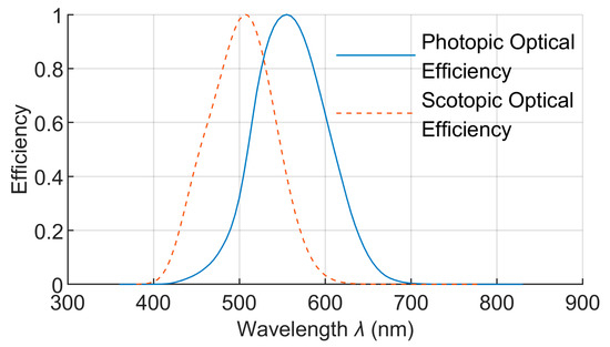
Figure 1.
Optical efficiency function.
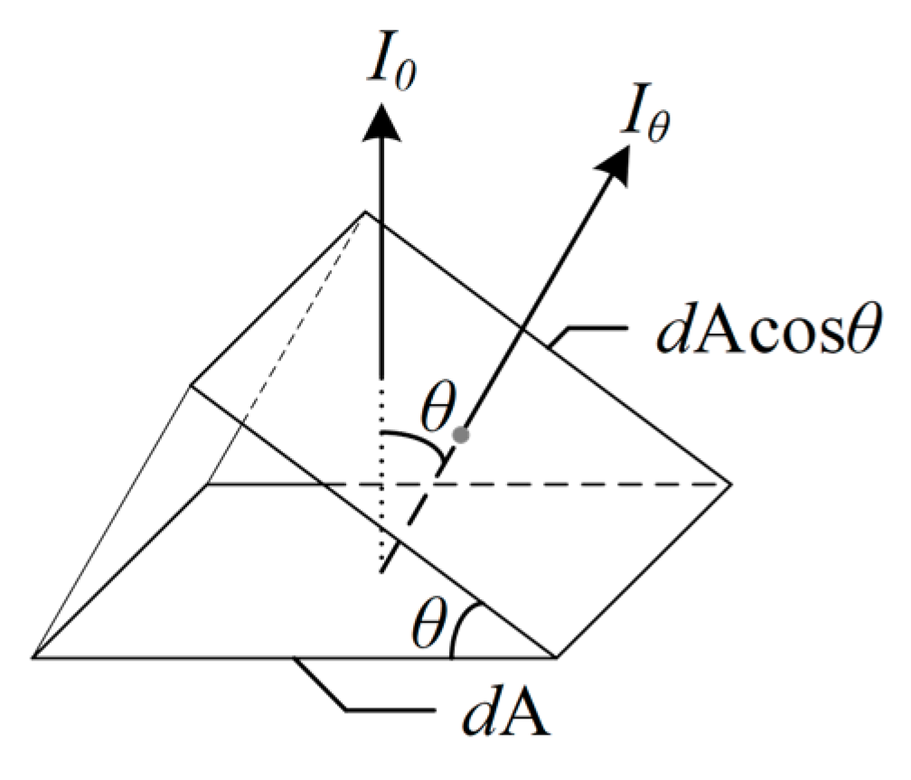
Luminous intensity indicates the illuminating characteristic of a light source in a given direction, which is defined as the magnitude of the luminous flux Φv per unit solid angle Ω in a given direction. The symbol is Iv and the unit is candela (cd):
Luminance indicates the illuminating characteristic of the illuminating surface in a given position and direction, which is defined as the illuminating intensity Iv per unit cross-section perpendicular to the direction. The symbol is Lv and the unit is candela per square meter (cd/m2):
where dA is the surface element of the beam section; θ is the angle between the normal of the surface element and the given direction, as shown in Figure 2.
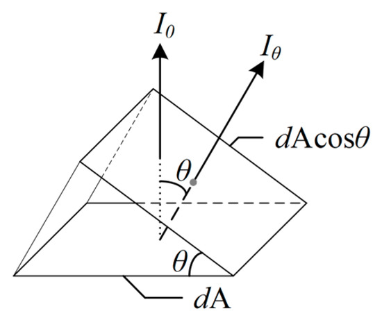
Figure 2.
Luminance definition.
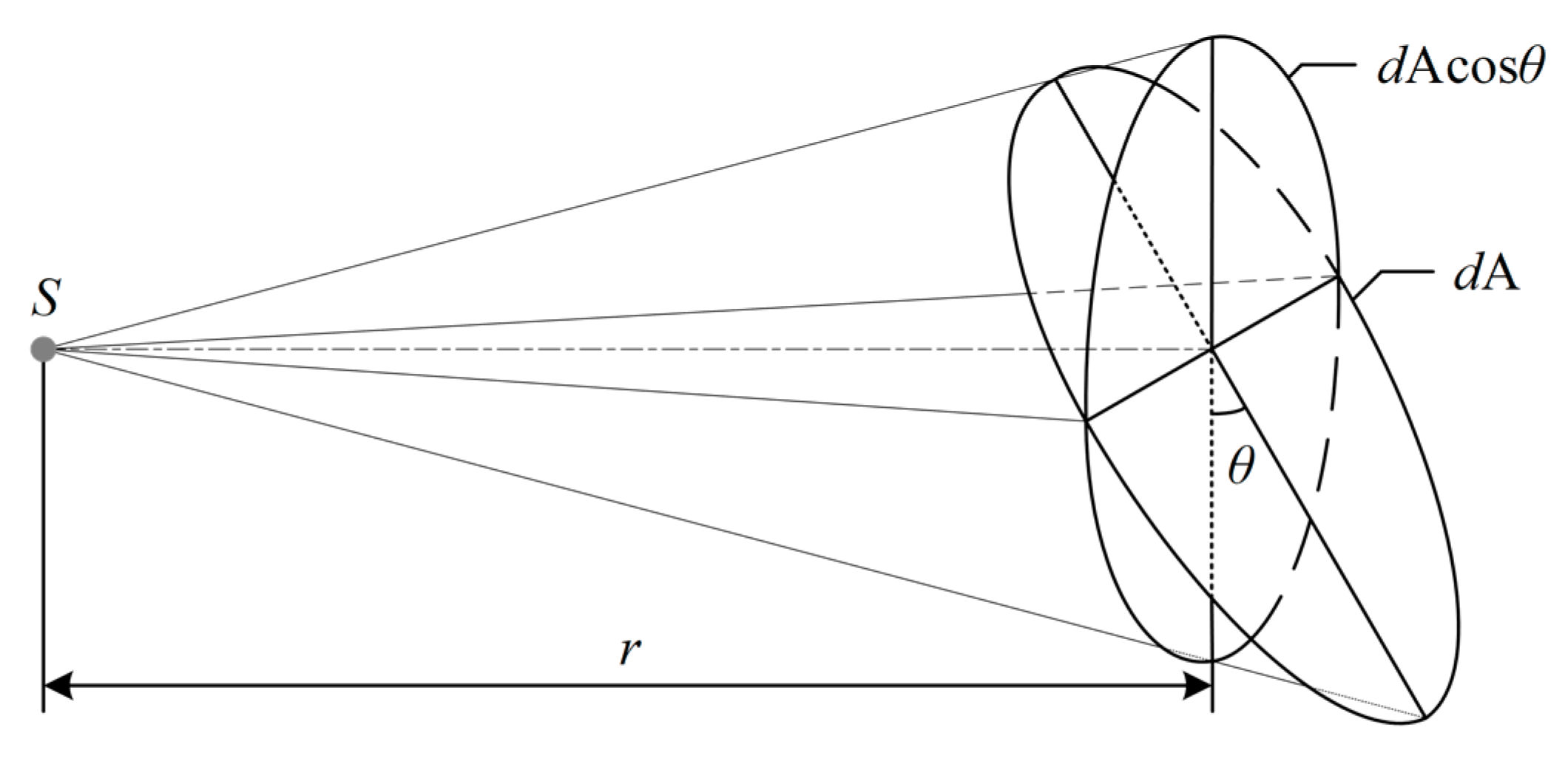
Illuminance indicates the light-receiving characteristic of the illuminated surface in a given position, which is defined as the luminous flux Φv received on the unit tangent plane on the fixed point. The symbol is Ev and the unit is lux (lx = cd·sr/m2):
where dA is the surface element of the tangent plane on the fixed point; θ is the angle between the normal of the surface element and the direction from the fixed point to the point source; r is the distance between the fixed point and the point source, as shown in Figure 3.
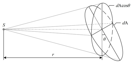
Figure 3.
Illuminance definition.
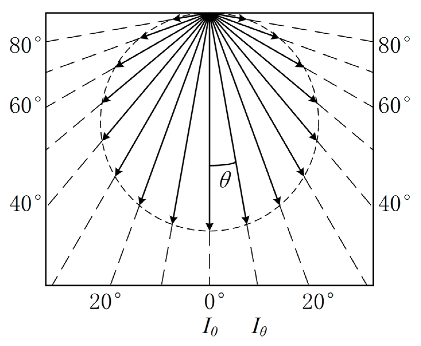
The luminous intensity of a standard Lambertian source (standard Lambertian surface) conforms to the law of cosine, as shown in Figure 4.
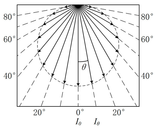
Figure 4.
Standard Lambertian source luminous intensity diagram.
The luminous intensity Iv,θ at a certain angle is equal to the light intensity Iv,0 in the axial direction of the light source multiplied by the cosine of the direction angle:
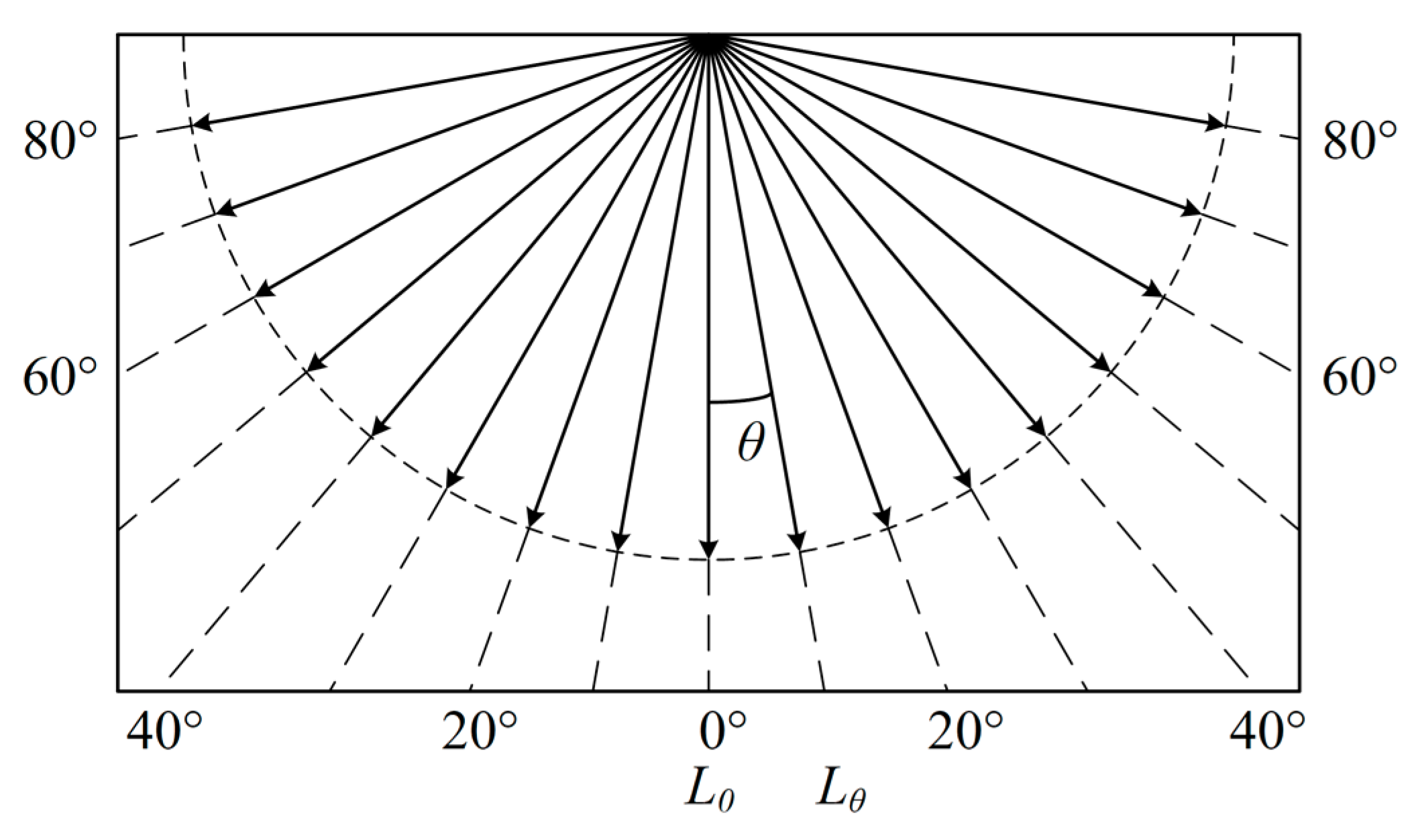
From Equations (3) and (5), the luminance of a standard Lambertian source (standard Lambertian surface) is independent of the direction, as shown in Figure 5:
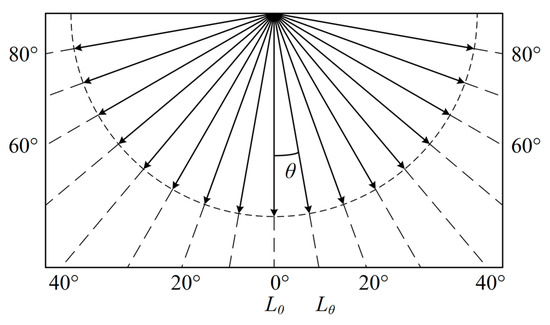
Figure 5.
Standard Lambertian source luminance diagram.
Symbolizing the luminance of a standard Lambertian source as Lv and the area as dA, the total luminous flux Φv radiated in the entire hemispherical surface, SP, is given in Equation (7):
Therefore, the luminous exitance Mv and the luminance Lv of a standard Lambertian source are in the following relationship:
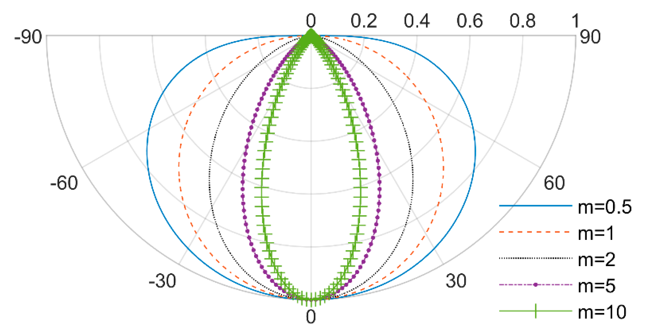
In the LED industry, people use the half power angle θ1/2 as a measure of the angle of illumination. The half power angle θ1/2 is defined as the angle between the axial direction and the direction in which the luminous intensity is half with the axial direction. From Equation (5), the half power angle θ1/2 of the standard Lambertian source is 60°.
In practical applications, the LED half power angle θ1/2 is often not equal to 60°. Such an LED is called a near-Lambertian light source, and the luminous intensity function is expressed as:
where m is the order of the Lambertian source. Combined with the definition of the half power angle θ1/2, the following is obtained:
So, we know that the order of the Lambertian source m and the half power angle θ1/2 correspond to each other. The order of the Lambertian source m can be obtained by the half power angle θ1/2, and the normalized luminous intensity distribution function curve is plotted, as shown in Figure 6.
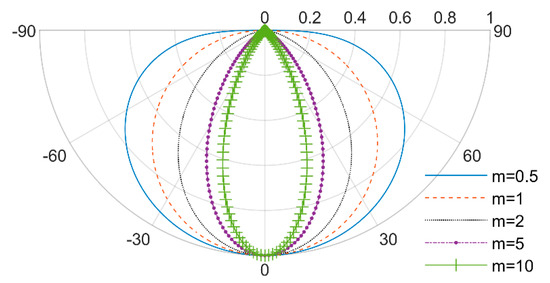
Figure 6.
Normalized near-Lambertian source luminous intensity diagram.
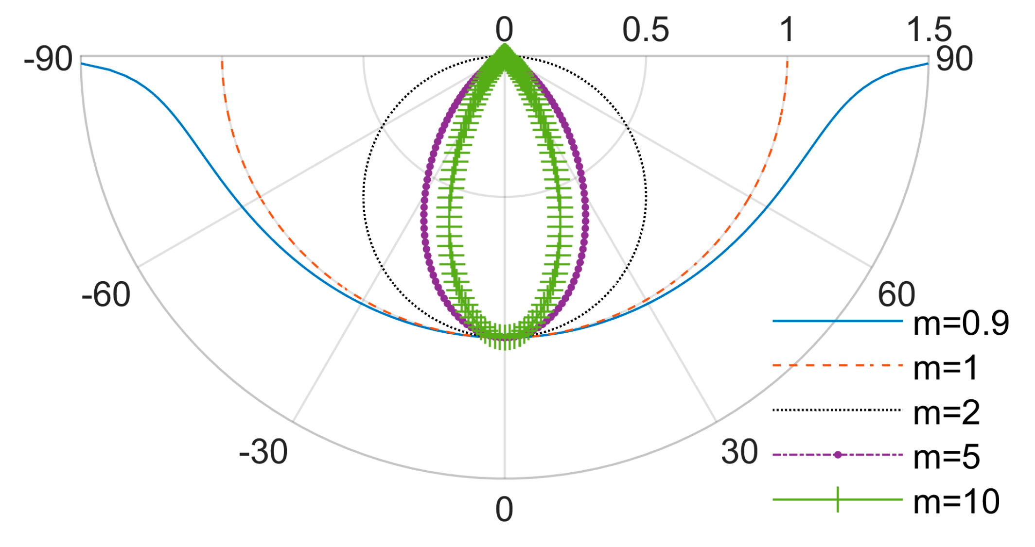
From Equations (3) and (9), the luminance of a near-Lambertian source is related to direction, and the normalized luminance distribution is shown in Figure 7:
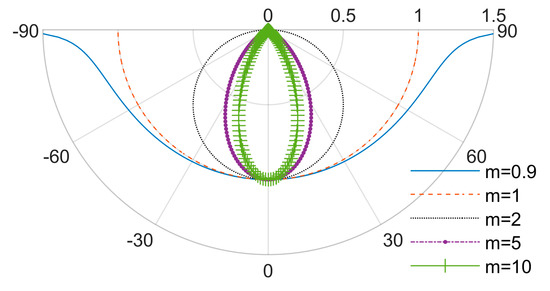
Figure 7.
Normalized near-Lambertian source luminance diagram.
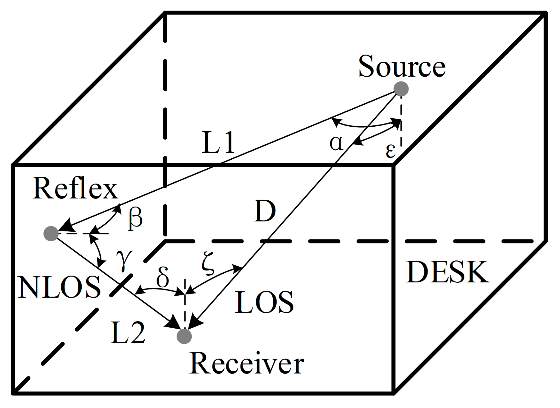
Figure 8 is a diagram of indoor VLC communication. We know that the indoor VLC communication links are divided into two categories: line of sight (LOS) and non-line of sight (NLOS). It has been proved that the proportion of the secondary reflected light to the total is too small [6]. In this paper, only direct light and first reflected light are considered.
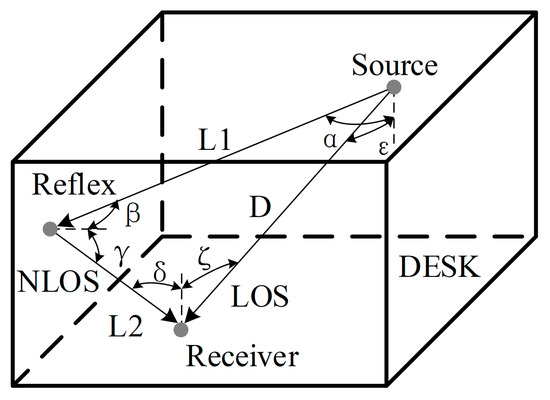
Figure 8.
Indoor visible light communication (VLC) communication diagram.
2.1. Horizontal Illuminance of LOS and NLOS
2.1.1. Horizontal Illuminance of LOS
From Equations (4) and (9), the horizontal illuminance of LOS, Ev,LOS, is known:
where I0 is the axial luminous intensity of LED lamps.
2.1.2. Horizontal Illuminance of NLOS
From Equation (12), the illuminance at the reflection point on the wall of NLOS, Ev,NLOS,Ref, is known:
From Equation (13), the luminous emittance at the reflection point on the wall of NLOS, Mv,NLOS,Ref, is known:
where ρ is the reflectivity of the wall.
From Equations (3), (8) and (14), the luminous intensity in the normal direction at the reflection point of NLOS, Iv,NLOS,Ref, is known:
where dAWALL is the reflective area of a small region.
From Equations (4), (5) and (15), the horizontal illuminance of NLOS, Ev,NLOS, is known:
2.2. Received Power of LOS and NLOS
Analogously to the definition of luminous intensity, in radiometry, the radiation intensity is defined as the radiant flux Φe per unit solid angle Ω in a given direction. The symbol is Ie and the unit is watts per solid angle (W/sr):
Because luminous intensity and radiation intensity are descriptions of the same physical phenomenon from different aspects, according to Equation (9), the radiation intensity of a near-Lambertian source can be assumed as follows:
where Vm is a variable associated with m and determining the relationship between Φe and Ie.
For a single-sided LED, the total radiant flux Φe radiated throughout the hemispherical surface SP can be calculated as:
From Equations (18) and (19), the radiant intensity Ie is known:
2.2.1. Received Power of LOS
From Equations (1), (12) and (20), the received power of LOS, PLOS, is known [6]:
where AR is the physical area of the detector in a photo diode (PD); PS is the transmitted optical power of the source; TS(ζ) is the gain of an optical filter; Ψc is the width of the field of vision (FOV) at a receiver; g(ζ) is the gain of an optical concentrator.
g(ζ) is known [6], and is given in Equation (22):
where n is the refractive index.
2.2.2. Received Power of NLOS
From Equations (1), (16) and (20), the received power of NLOS, PNLOS, is known [6]:
2.3. Channel Quality
Channel noise is divided into three parts: ISI noise, shot noise, and thermal noise.
In the indoor VLC communication system, the signal-to-noise ratio at the receiving end is expressed as follows [6]:
where γ is the detector responsivity; PrSignal is the signal power; σ2shot is the shot noise; σ2thermal is the thermal noise; PrISI is the ISI noise power.
2.3.1. ISI Noise
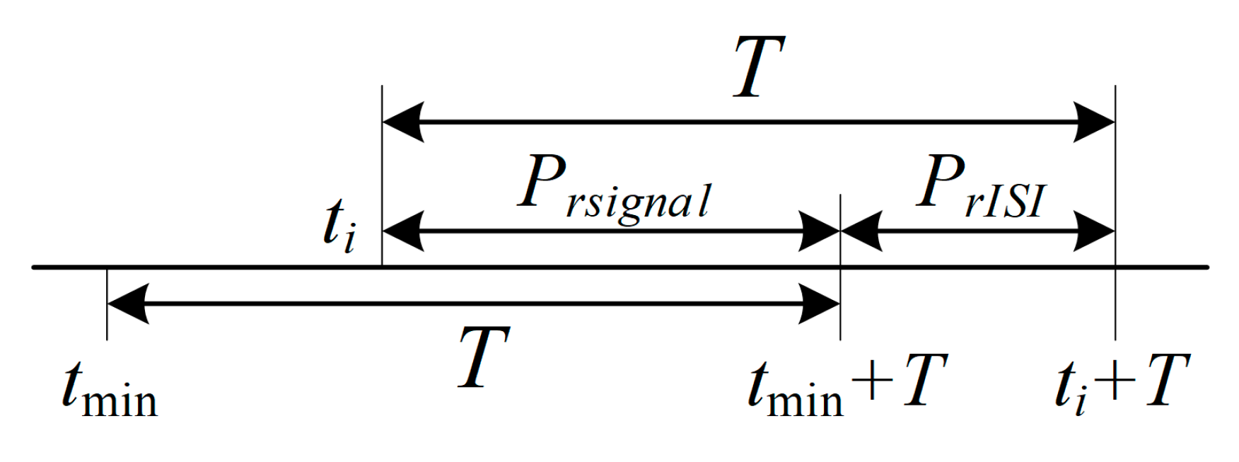
ISI noise is caused by ISI power. In a VLC system, the power received by the PD is divided into signal power and ISI power. When a signal is transmitted, during the first arriving signal operation, the power of all the paths is the signal power. After the first arriving signal is completed, the power of all the paths is the ISI power, as shown in Figure 9.
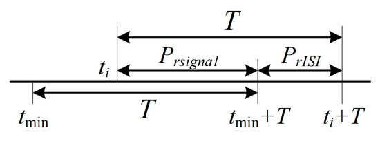
Figure 9.
Signal power and inter-symbol interference (ISI) power diagram.
In Figure 9, tmin is the earliest arrival time of the signals in all paths, ti is the arrival time of the signal in the path, and T is the symbol period.
2.3.2. Shot Noise
Shot noise originates from active components in electronic devices and is caused by uneven electron emission. In this system, it results from the photocurrent caused by LED illumination and the dark current caused by ambient illumination.
The shot noise caused by LED illumination, σ2shot,LED, is known [6]:
where q is the electronic charge; B is equivalent noise bandwidth, and it is equal to the data rate.
The shot noise caused by ambient illumination, σ2shot,bg, is known [6]:
where Ibg is background current; I2 is one of the noise band width factors.
2.3.3. Thermal Noise
Thermal noise is also called resistance noise, originates from passive components in electronic devices, and is caused by electronic Brownian motion. In this system, it results from feedback resistors and field effect transistor (FETs).
The thermal noise resulting from feedback resistors, σ2thermal,Res, is known [6]:
where k is Boltzmann’s constant; Tk is the absolute temperature; η is the fixed capacitance of the photo detector per unit area; G is the open-loop voltage gain; AR is the physical area of the detector in a PD; B is equivalent noise bandwidth, and it is equal to the data rate.
The thermal noise resulting from FETs, σ2thermal,FET, is known [6]:
where Γ is the FET channel noise factor; I3 is one of the noise band width factors; gm is the FET transconductance; η is the fixed capacitance of the photo detector per unit area; AR is the physical area of the detector in a PD; B is the equivalent noise bandwidth, and it is equal to the data rate.
3. Simulation Data and LED Layouts
This section is divided into two parts. The first part describes the data used in the simulation. The second part determines the three different LED layouts (normal, optimal illumination, optimal channel quality). All the simulations in this paper were completed using MATLAB software.
3.1. Simulation Data
3.1.1. Conventional LED Layout Model
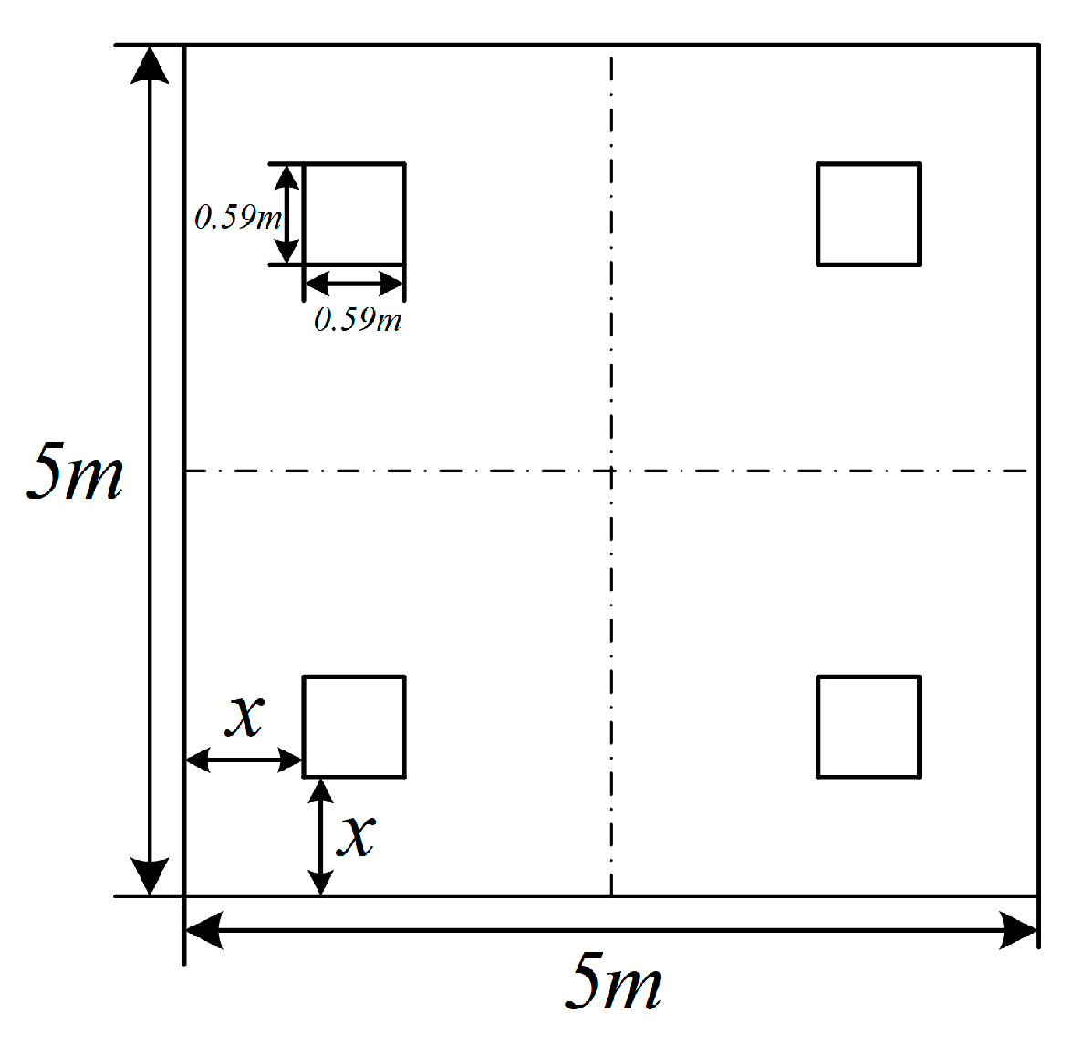
The conventional indoor LEDs layout model is shown in Figure 10. The room size is 5 m × 5 m, the height of the table is 0.75 m from the floor, and the height of the lamps’ light is 2.5 m from the floor. The four lamps are symmetrically distributed in the room, and each lamp consists of 60 × 60 LED chips with a pitch of 0.01 m [6].
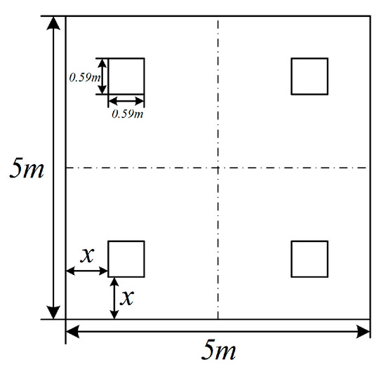
Figure 10.
Light-emitting diode (LED) layout model diagram.
From Figure 10, it is known that if the distance x between the edge of one of the lamps and the edge of the adjacent wall is determined, the overall layout of the indoor LEDs is uniquely determined.
3.1.2. Simulation Parameter
The simulation settings are shown in Table 1.

Table 1.
Simulation calculation settings.
The parameters of the LED chips are shown in Table 2.
Table 2.
Parameters of the LED chips.
The parameters of the PDs are shown in Table 3.
Table 3.
Parameters of the photo diodes (PDs).
The parameters of the noise calculation are shown in Table 4.
Table 4.
Parameters of the noise calculation.
3.2. LED Layout
3.2.1. Normal Layout
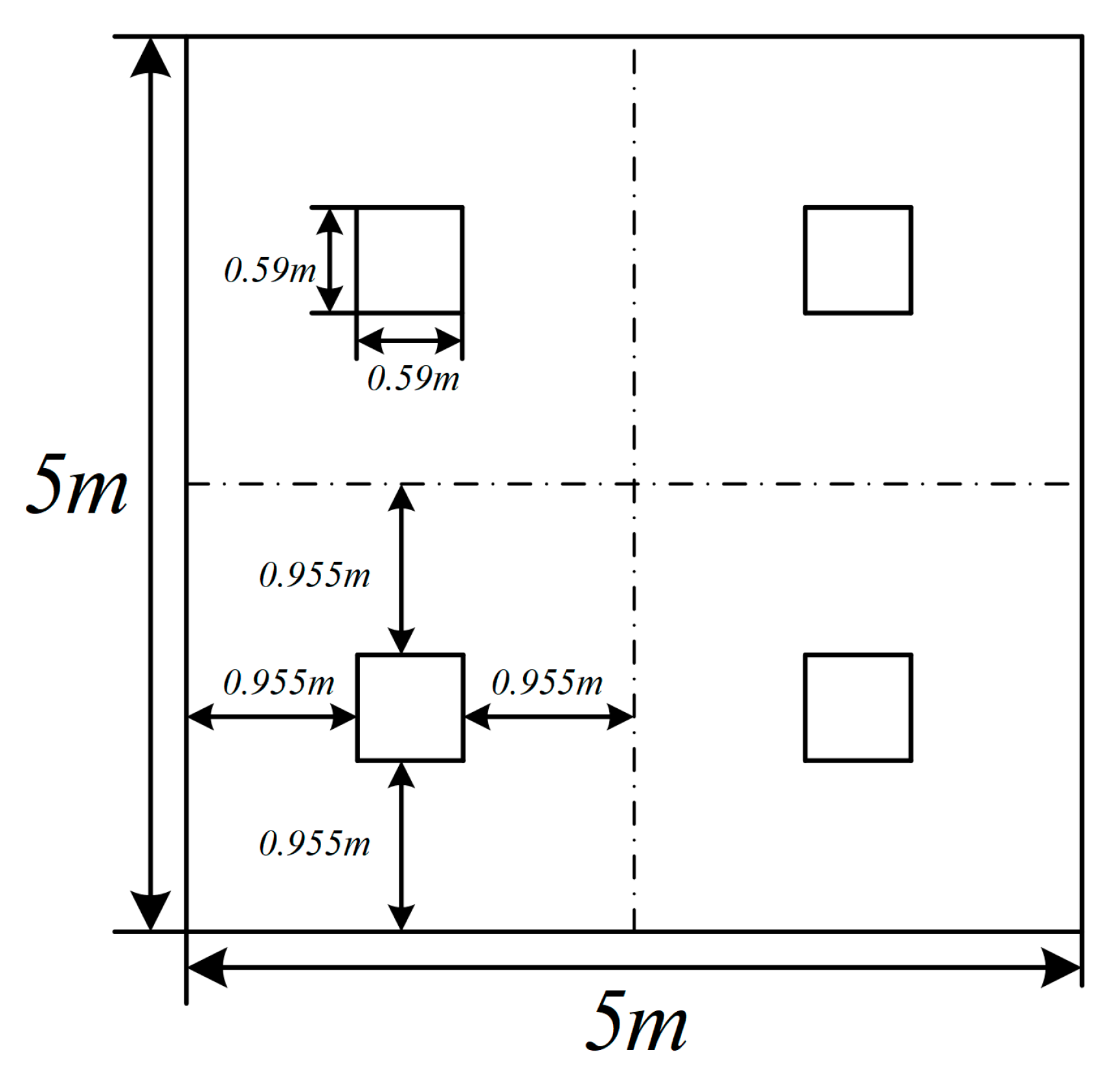
The normal layout is the equally spaced layout used in [6]. Each lamp is located at the center of the respective area, and x is 0.955 m, as shown in Figure 11.
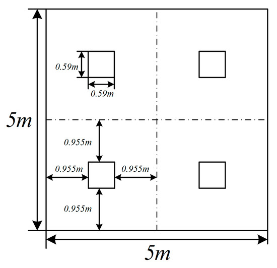
Figure 11.
Normal layout diagram.
3.2.2. Optimal Layout of Illumination
Drawing on existing literature [2], we use the parameter QE to evaluate the horizontal illuminance.
where is the mean of horizontal illuminance; var(Ev) is the variance of horizontal illuminance. The larger QE is, the more uniform the horizontal illumination distribution will be.
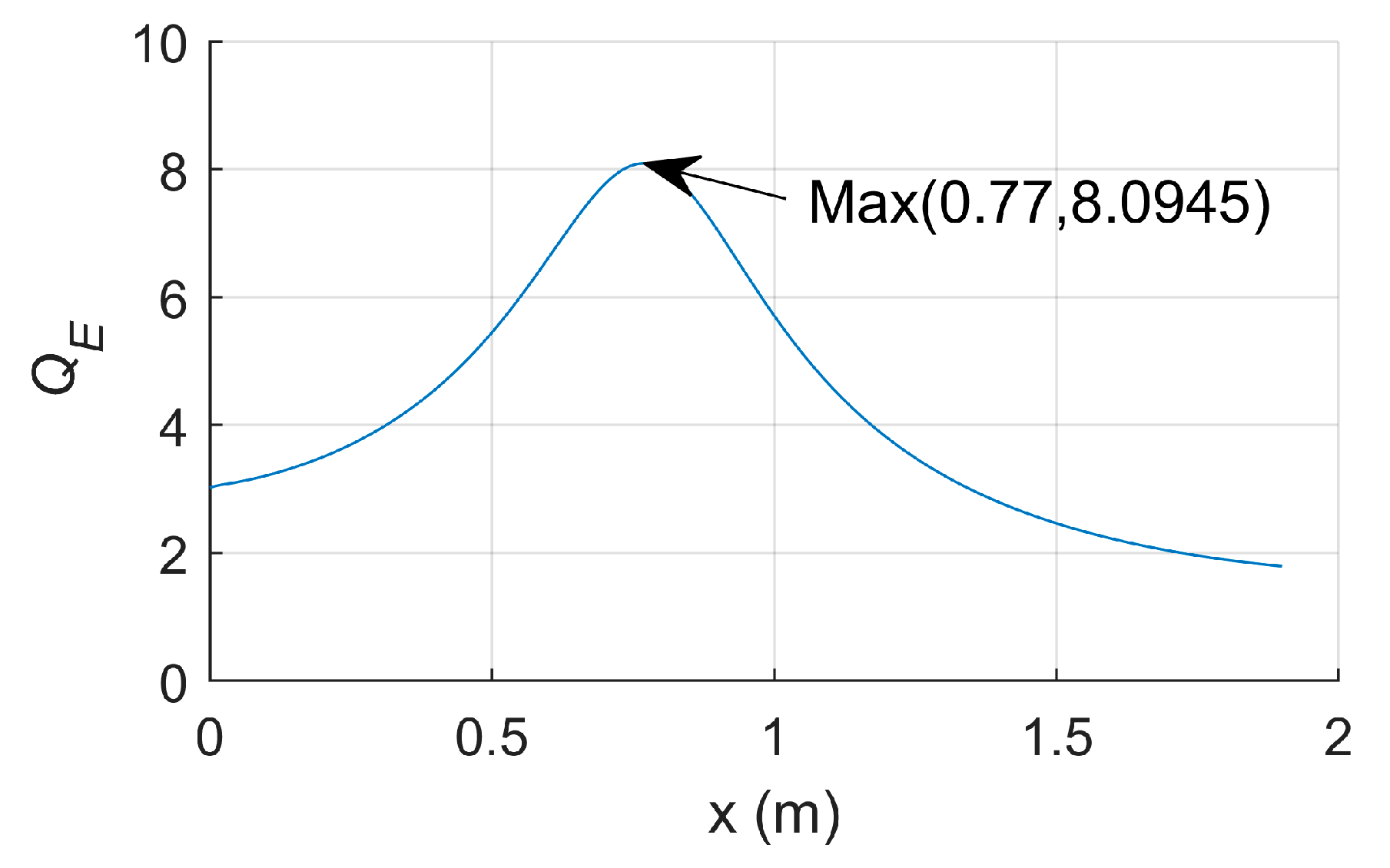
The relationship between x and QE is shown in Figure 12. As can be seen from the figure, when x is 0.77 m, QE reaches the maximum value of 8.0945, meaning that this LED layout is the optimal layout of illumination under the conventional indoor LED layout model.
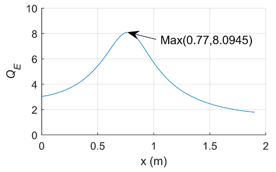
Figure 12.
Relationship between x and QE.
3.2.3. Optimal Layout of Channel Quality
Drawing on existing literature [4], we use the parameter QSNR to evaluate the channel quality.
where is the mean of the SNR; var(SNR) is the variance of the SNR. The larger QSNR is, the more uniform the SNR distribution will be.
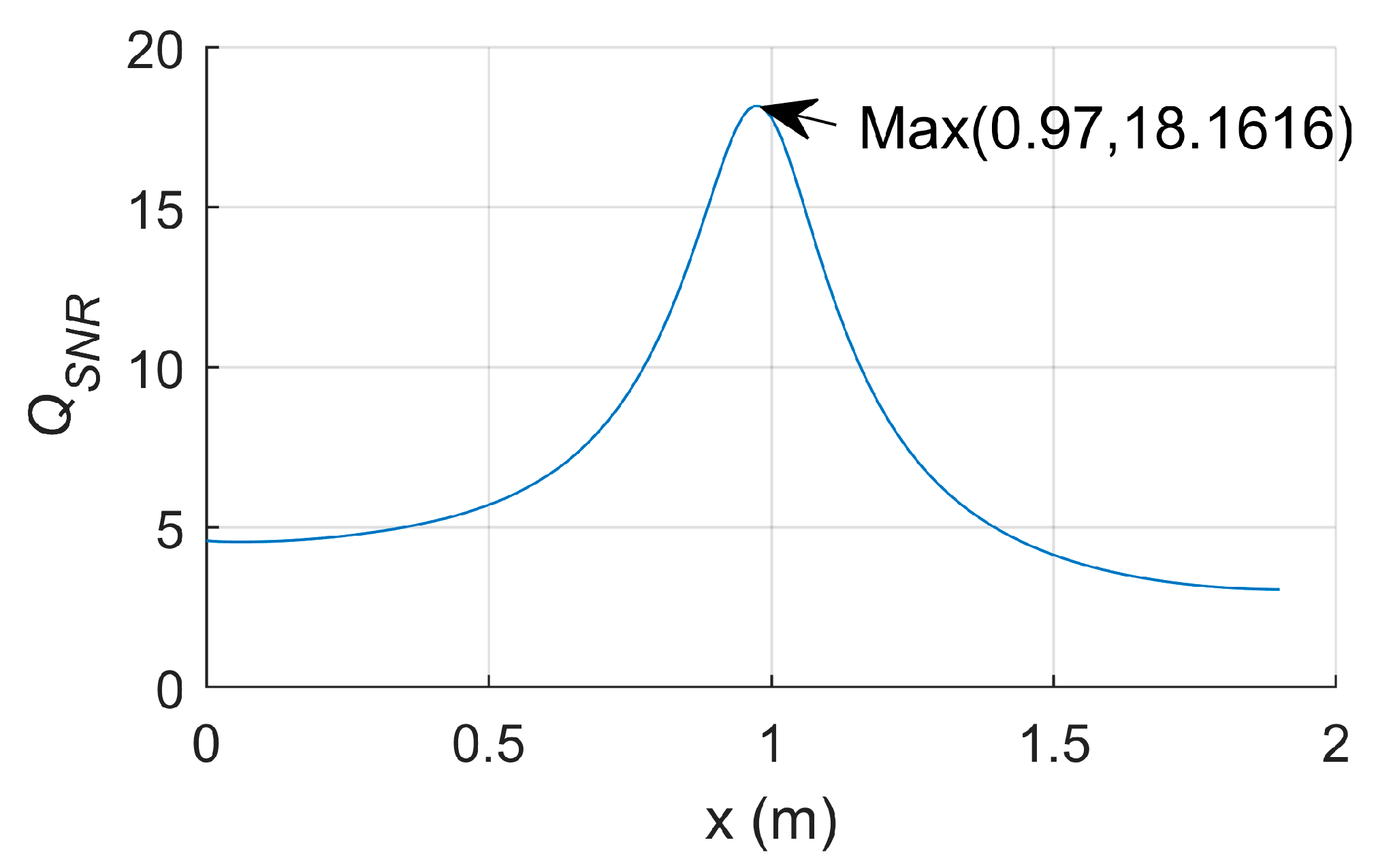
The relationship between x and QSNR is shown in Figure 13. As can be seen from the figure, when x is 0.97 m, QSNR reaches the maximum value of 18.1616, meaning that this LED layout is the optimal layout of channel quality under the conventional indoor LED layout model.
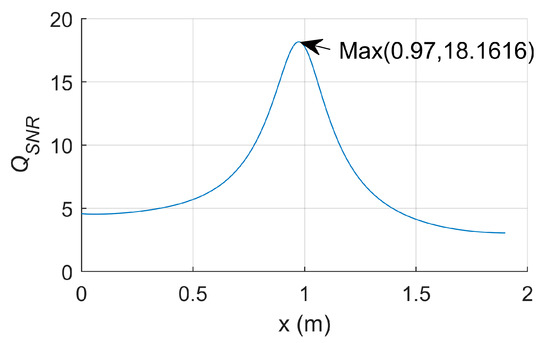
Figure 13.
Relationship between x and QSNR.
4. Data Analysis
In Section 3, three kinds of LED layouts were determined. In this section, we compare and analyze the illuminance distribution, SNR distribution, M-DS distribution, and IR of the three layouts.
4.1. Illuminance Distribution
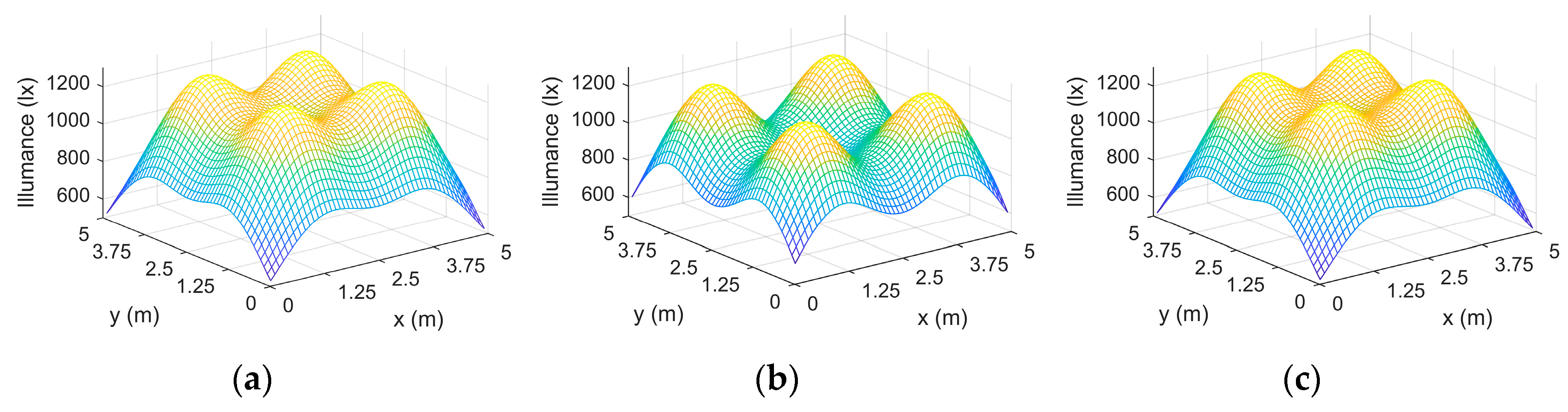
The illuminance distribution of the three different LED layouts is simulated. The simulation results are shown in Figure 14, and the data comparison is shown in Table 5.
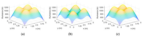
Figure 14.
Illuminance distribution: (a) the illuminance distribution of the normal layout; (b) the illuminance distribution of the optimal layout of illumination; (c) the illuminance distribution of the optimal layout of channel quality.
Table 5.
Illuminance data comparison.
In Section 3, we found that the normal layout and the optimal layout of channel quality are so similar that the difference in the data of illuminance distribution of these layouts is too small. The standard deviation (STD) of the optimal layout of illumination is reduced by 42.7798 and 48.7914 to 120.4515 lx compared with the normal layout’s 163.2313 lx and the optimal layout of channel quality’s 169.2429 lx.
In general, the illuminance distribution of the three layouts meets the standards of the International Organization for Standardization [8]. However, it is recommended to use the optimal layout of illumination in applications with high illumination uniformity requirements.
4.2. SNR Distribution
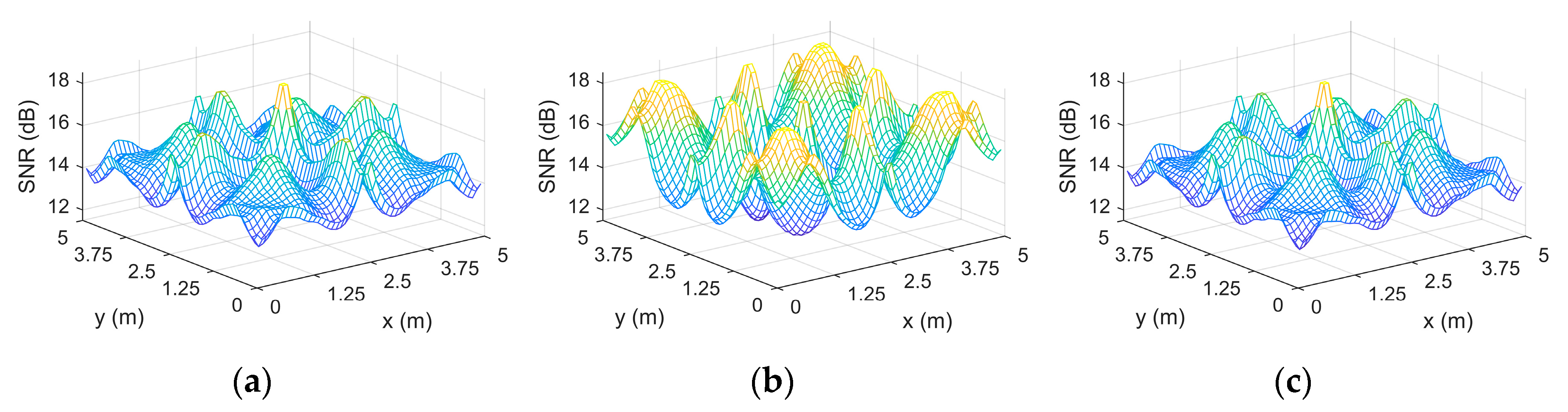
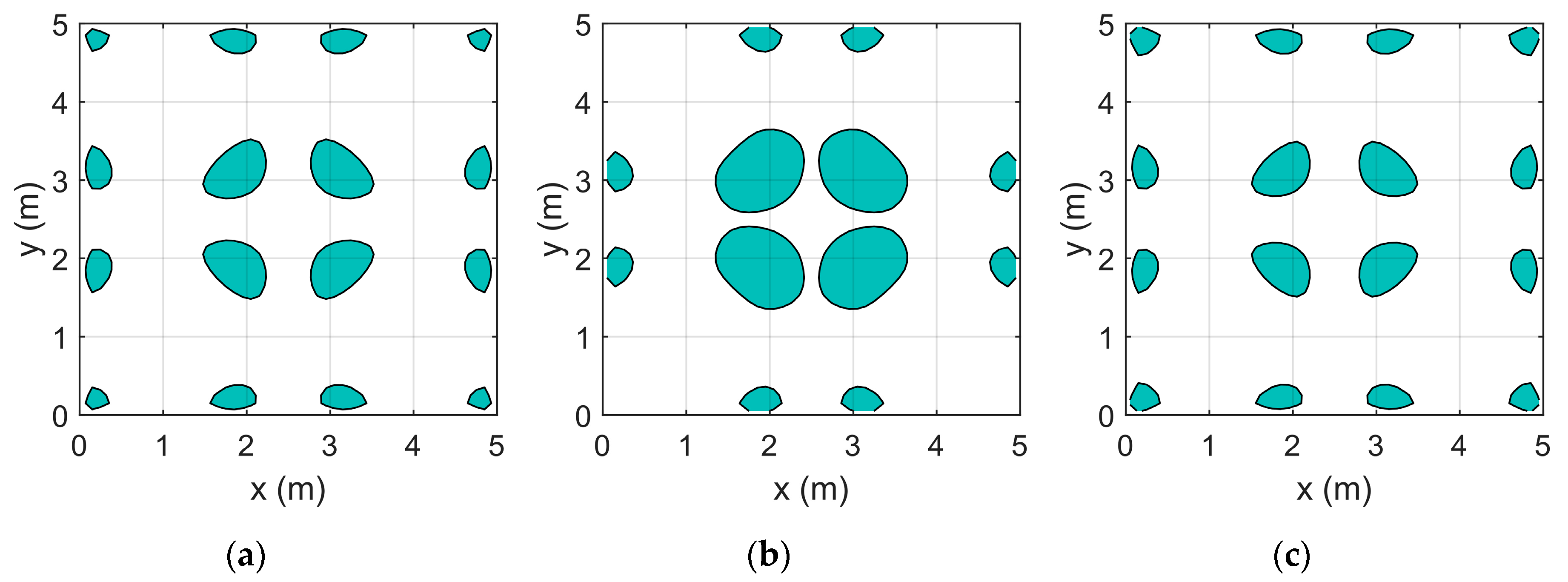
The SNR distribution of the three different LED layouts is simulated. The simulation results are shown in Figure 15. A received optical power of SNR = 13.6 dB is required for a stable communication link [6]. In Figure 16, the dark area is the area in which SNR < 13.6 dB. The data comparison is shown in Table 6.

Figure 15.
Signal-to-noise ratio (SNR) distribution: (a) the SNR distribution of the normal layout; (b) the SNR distribution of the optimal layout of illumination; (c) the SNR distribution of the optimal layout of channel quality.
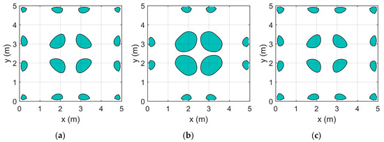
Figure 16.
Noneffective area distribution: (a) the noneffective area distribution of the normal layout; (b) the noneffective area distribution of the optimal layout of illumination; (c) the noneffective area distribution of the optimal layout of channel quality.
Table 6.
SNR data comparison.
From Table 6, the effective area percentage of the optimal layout of channel quality is increased by 0.32% and 6.08% to 88.80% as compared with the normal layout’s 88.48% and the optimal layout of illumination’s 82.72%. The STD of SNR distribution of the optimal layout of channel quality is reduced by 0.0116 and 0.7338 to 0.7978 dB as compared with the normal layout’s 0.8094 dB and the optimal layout of illumination’s 1.5316 dB. The minimum SNR distribution of the optimal layout of channel quality is increased by 0.1138 and 1.1945 to 13.0040 dB as compared with the normal layout’s 12.8902 dB and the optimal layout of illumination’s 11.8095 dB.
In general, the normal layout and the optimal layout of channel quality are so similar that both of them can be chosen in general practical applications, but it is recommended to use the optimal layout of channel quality in applications with high SNR standards.
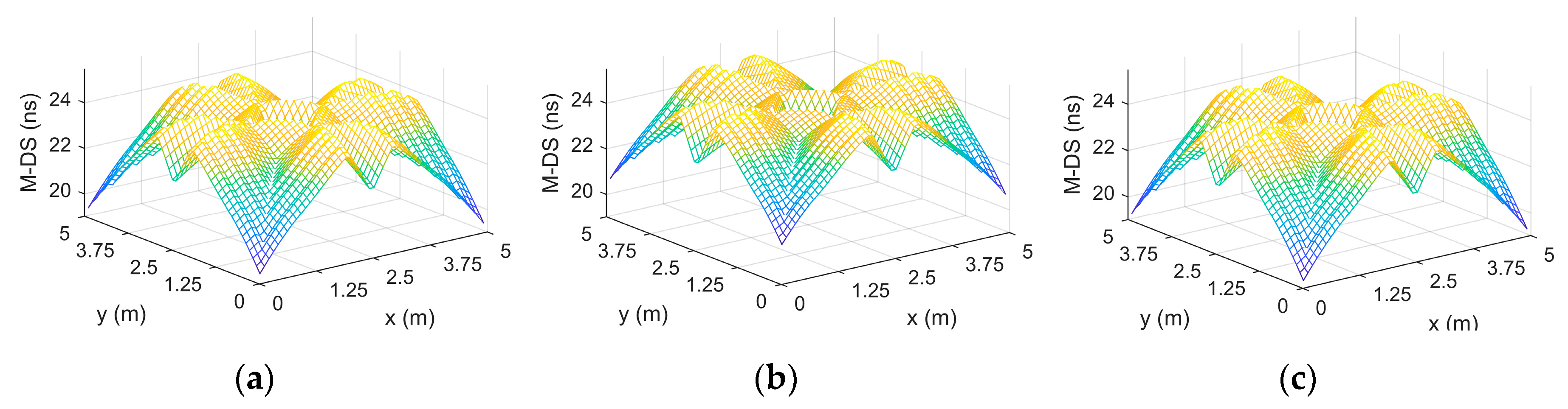
4.3. M-DS Distribution
In an indoor VLC system, there are lots of different channel paths; the arrival time of the signals via the paths differs due to the different path lengths, and the pulse width of the received signal is widened due to the multipath effect. The phenomenon is called delay spread.
Differently from most existing literature [1,2,5], in this paper, we consider the effect of FOV in M-DS distribution, so we get something new.
The M-DS refers to the difference in arrival time between the earliest arrival signal and the latest arrival signal. The M-DS distribution of the three different LED layouts is simulated. The simulation results are shown in Figure 17 and the data comparison is shown in Table 7.
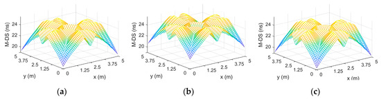
Figure 17.
Maximum delay spread (M-DS) distribution: (a) the M-DS distribution of the normal layout; (b) the M-DS distribution of the optimal layout of illumination; (c) the M-DS distribution of the optimal layout of channel quality.
Table 7.
M-DS data comparison.
By comparing Figure 15 and Figure 17, we find that, in general, where M-DS is smaller, SNR is larger. As for the difference in the data in the corner, it can be explained by the FOV. Due to the presence of the FOV, most signals with a long transmission path in the corner are not within its FOV and, therefore, not recorded, resulting in a large drop in the M-DS at that location. The same reason causes the ISI noise power and the signal power at the position to be correspondingly reduced, while the shot noise and thermal noise are constant. All these result in the M-DS in the corner being the shortest, but the SNR in the same position not being large.
From Table 7, the minimum M-DS distribution of the optimal layout of channel quality is reduced by 0.1093 and 1.4204 to 19.2880 ns as compared with the normal layout’s 19.3973 ns and the optimal layout of illumination’s 20.7084 ns. The mean of the M-DS distribution of the optimal layout of channel quality is reduced by 0.0706 and 0.8962 to 22.8768 ns as compared with the normal layout’s 22.9474 ns and the optimal layout of illumination’s 23.7730 ns. The maximum M-DS distribution of the optimal layout of channel quality is reduced by 0.0549 and 0.7744 to 24.2783 ns as compared with the normal layout’s 24.3332 ns and the optimal layout of illumination’s 25.0527 ns.
4.4. Impulse Response
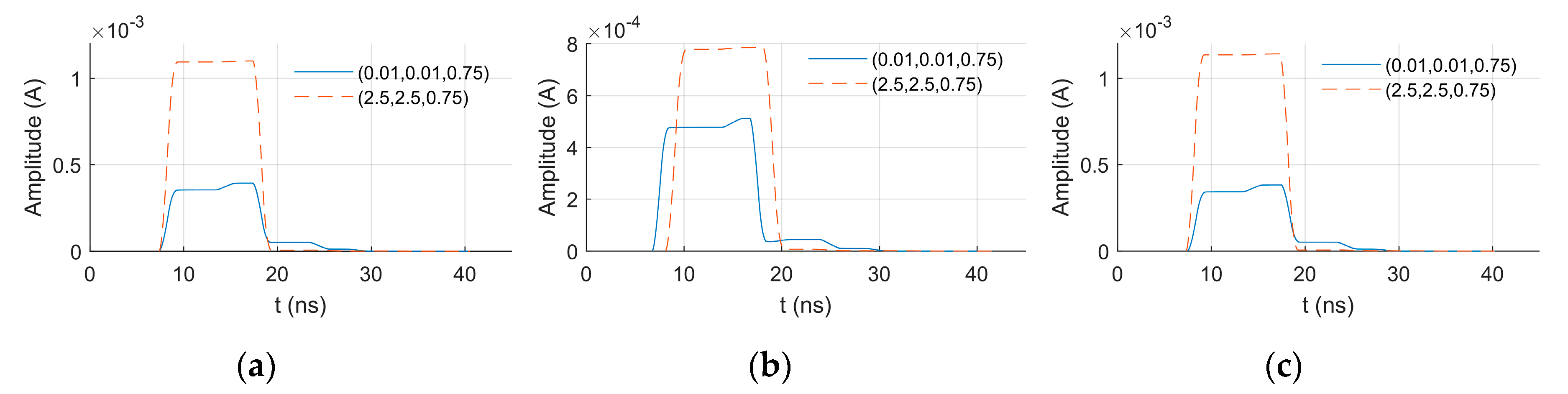
The impulse response of the three different LED layouts is simulated. The simulation results are shown in Figure 18.
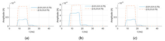
Figure 18.
Impulse response: (a) the impulse response of the normal layout; (b) the impulse response of the optimal layout of illumination; (c) the impulse response of the optimal layout of channel quality.
Since the layouts of the normal layout and the optimal layout of channel quality are too close, the impulse responses of these are also similar. From Figure 18, there is no significant delay between the impulse response of the normal layout (optimal layout of channel quality) at the center and corner, and the difference between the amplitude of the two is large. There is a significant delay between the impulse response of the optimal layout of illumination at the center and corner, and the difference between the amplitudes of the two is smaller.
5. Conclusions
Considering the first reflected light, based on the conventional layout model and the classic indoor VLC model, we first defined the parameter Q and then drew the corresponding curve of the layout and the parameter Q, thus determining the optimal layout of illumination and the optimal layout of channel quality. Combined with the normal layout, three layouts were determined. Later, an illuminance distribution simulation, SNR distribution simulation, M-DS distribution simulation, and IR simulation were performed for each layout. The achieved results show that the illuminance distributions of the three layouts meet the standards of the International Organization for Standardization. In the SNR distribution, M-DS distribution, and impulse response, the optimal layout of channel quality is obviously better than the optimal layout of illumination. In particular, the effective area percentage of the optimal layout of channel quality is increased by 0.32% and 6.08% to 88.80% as compared with the normal layout’s 88.48% and the optimal layout of illumination’s 82.72%. However, compared with the normal layout, the advantages are not very prominent.
Author Contributions
Conceptualization, X.Z. and N.Z.; methodology, X.Z.; resources, X.Y.; data curation, X.Z.; writing—original draft preparation, X.Z.; writing—review and editing, M.B.K.; supervision, F.A.-T. and X.Y.; project administration, X.Y.; funding acquisition, X.Y. All authors have read and agreed to the published version of the manuscript.
Funding
This research was funded by National Natural Science Foundation of China, grant number 61301175.
Conflicts of Interest
The authors declare no conflict of interest.
References
- Ding, J.; Huang, Z.; Ji, Y. Evolutionary Algorithm Based Power Coverage Optimization for Visible Light Communications. IEEE Commun. Lett. 2012, 16, 439–441. [Google Scholar] [CrossRef]
- Wang, Z.; Yu, C.; Zhong, W.-D.; Chen, J.; Chen, W. Performance of a novel LED lamp arrangement to reduce SNR fluctuation for multi-user visible light communication systems. Opt. Express 2012, 20, 4564–4573. [Google Scholar] [CrossRef] [PubMed]
- Borogovac, T.; Rahaim, M.; Carruthers, J.B. Spotlighting for visible light communications and illumination. In Proceedings of the 2010 IEEE Globecom Workshops, Miami, FL, USA, 6–10 December 2010; pp. 1077–1081. [Google Scholar] [CrossRef]
- Wu, D.; Ghassemlooy, Z.; Leminh, H.; Rajbhandari, S.; Kavian, Y.S. Power distribution and Q-factor analysis of diffuse cellular indoor visible light communication systems. In Proceedings of the 16th European Conference on Networks and Optical Communications, Newcastle upon Tyne, UK, 20–22 July 2011; pp. 28–31. [Google Scholar]
- Wu, D.; Ghassemlooy, Z.; Le Minh, H.; Rajbhandari, S.; Khalighi, M.A. Optimisation of Lambertian order for indoor non-directed optical wireless communication. In Proceedings of the 2012 1st IEEE International Conference on Communications in China Workshops (ICCC), Beijing, China, 15–17 August 2012; pp. 43–48. [Google Scholar]
- Komine, T.; Nakagawa, M. Fundamental analysis for visible-light communication system using LED lights. IEEE Trans. Consum. Electron. 2004, 50, 100–107. [Google Scholar] [CrossRef]
- Shen, Z.; Lan, T.; Wang, Y.; Wang, L.; Ni, G. Simulation and analysis for indoor visible-light communication based on LED. Infrared Laser Eng. 2015, 44, 2496–2500. [Google Scholar]
- ISO. Lighting of Indoor Work Places; ISO 8995:2002(E)/CIE S 008/E-2001; ISO: Geneva, Switzerland, 2002. [Google Scholar]
Publisher’s Note: MDPI stays neutral with regard to jurisdictional claims in published maps and institutional affiliations. |
© 2020 by the authors. Licensee MDPI, Basel, Switzerland. This article is an open access article distributed under the terms and conditions of the Creative Commons Attribution (CC BY) license (http://creativecommons.org/licenses/by/4.0/).