1. Introduction
Renewable energy solutions such as wind-based or solar-based installations are selected depending on the characteristics of the geographical zone. In particular, the photovoltaic (PV) systems are an interesting alternative for any scenario since the energy source is the incident solar irradiance, which is widely available, and the PV systems require much less maintenance in comparison with wind-based solutions or other options with moving parts [
1].
The harvesting of solar energy using PV panels requires the use of power converters to extract the maximum available power, where the buck and boost converters are the most commonly adopted [
2,
3]. Moreover, the energy extraction from PV systems requires a maximum power point tracking (
MPPT) technique [
4], which defines the operating condition of both PV module and dc/dc converter depending on the weather conditions. It is common to connect several PV modules in series, which are connected to a single power converter to perform the
MPPT action; however, this structure can lead to mismatching conditions among the modules [
5], such as partial shading, thus reducing the global energy production. On the other hand, it is possible to interface each PV module with dedicated power converter and
MPPT algorithm, which is known as distributed maximum power point tracking (DMPPT) system. Those DMPPT systems increase the efficiency of the PV system [
6] by avoiding the mismatching problem, and also increase the system reliability by isolating each PV panel from the failures of the other ones. In commercial installations, DMPPT systems are usually implemented using microinverters, which require a first stage based on dc/dc converters with high elevation and high efficiency [
7].
The design of the dc/dc stage in PV microinverters can be done using a cascade connection of boost converters to reach the required gain. This requires a large number of semiconductor and passive elements in the power conversion stage, and those cascade converters are frequently regulated using independent controllers, thus the efficiency may be negatively affected [
8]. To avoid this problem, the dual active bridge (DAB) converter has been designed, which provides high elevation, high efficiency, galvanic isolation, bidirectional power flow, and buck-boost voltage operation [
9]. This dc/dc converter has an internal ac stage, which is based on two semiconductor bridges and a high frequency transformer, thus it is able to provide a voltage conversion ratio much higher in comparison with a series connection of boost converters [
10].
Another important part of PV systems is the controller of the PV voltage [
11]. Such a controller regulates the power converter to ensure that the PV voltage or current follows the reference provided by the
MPPT algorithm even in presence of perturbations, such as changes on the solar irradiance, changes on the ambient temperature, load changes, among others [
12]. The design of those control systems is usually based on a mathematical representation of the PV system, which could be a nonlinear model or a linearized one [
13]. Therefore, to design PV voltage (or current) controllers for a PV system based on the DAB converter, it is necessary to develop a mathematical model to describe the dynamic behavior of the PV system.
Different approaches to model the DAB converter have been proposed in literature; one of them is to model the converter based on the analysis of different waveforms. In particular, this method consists in describing the changes occurring in a single switching period, which are formalized using equations for some points of interest. For example, in [
14] the authors proposed to model the peak and RMS values of leakage inductor current (
in
Figure 1) and the average current flowing through each transistor of the converter (
–
in
Figure 1). That model is oriented for aerospace applications, where the DAB converter is connected between a voltage source and an ultracapacitor. A similar waveform analysis was reported in [
15], where the relation between
and the output current of the converter is modeled to regulate a resistive load powered by voltage source. This work, validates the model by contrasting both predicted and experimental waveforms, in time and frequency domain, to demonstrate the correct prediction of the converter behavior.
Another modeling methodology used for DAB converters is based on equivalent circuits, which is aimed at representing the DAB converter with fewer elements; in this way, it is possible to simplify the nodal analysis of the circuit. For example, the work reported in [
16] was focused in DAB converters for marine applications, where the equivalent circuit consists of a square waveform source representing the voltage of
(first bridge in
Figure 1) followed by the leakage inductor of the high frequency transformer (HFT), and at the other end another square waveform source representing the voltage of
(second bridge in
Figure 1). That model is validated by contrasting the open-loop response of both the model and the experimental circuit. The same modeling technique was also applied in [
17] to model a Quad-Active-Bridge (QAB) converter interacting with a battery bank, a rectifier, a PV source and an inverter. The proposed equivalent circuit reports two DAB converters linked with a unified HFT, but the PV source model is not analyzed; moreover, the circuit does not take into account the protection diodes required to avoid the current flow into the PV panels from the QAB converter, which could destroy the PV source due to dissipative heating. This model was validated by comparing both time and frequency responses of the model and the non-linear circuit, and using the linearized model to design classical control systems.
A third modeling approach applied to the DAB converter is based on the Fourier analysis. This modeling technique requires to perform a circuital analysis using the Kirchoff’s laws; then, those electrical equations are decomposed using the Fourier transformation. An example of this modeling technique is presented in [
18], which is focused on a DAB converter interacting with a voltage source at one terminal and a Norton load at the other terminal. The main objective of that work is to obtain a linearized model of the system for control purposes, where the resulting equations describe the output (load) voltage and the leakage inductor current. Such a model is validated by comparing the model predictions with the response of a reference circuit in frequency domain, suggesting that the model is appropriate for control design. Similarly, the Fourier analysis was applied in [
19] to model a DAB converter interacting with a voltage source and a dc load. That model equations are focused on representing the output (load) voltage and the leakage inductor current, where a first result is the large-signal model of the system. A second result consist in a small-signal model of the system, which could be used to design classical control systems for the output voltage or current. Finally, the Fourier analysis technique is useful to extract low-order expressions from the electrical equations, which could simplify those expression into compact models useful for control design.
However, there is not reported in literature a control-oriented model for PV systems based on DAB converters, which also includes the protection diodes needed to avoid input current flows into the PV array, and the connection with a dc bus usually adopted in microinverters and microgrids. Therefore, this paper addresses such a problem by introducing the following contributions: first, a mathematical model of the DAB converter interacting with a PV module and a dc bus, including the protection diodes, which can be used to design non-linear controllers; second, a linearized version of the model oriented to design classical control systems; and third, an application example of the model aimed at ensuring the optimal power extraction of the PV system.
The rest of the paper is organized as follows:
Section 2 describes the basic circuit, operation and waveforms of the DAB converter; then,
Section 3 presents the proposed modeling approach for the PV system based on a DAB converter (first and second contributions).
Section 4 validates the accuracy of the proposed models using circuital simulations in both the time domain and frequency domain, and
Section 5 confirms the usability of the proposed model for designing control systems, illustrating the design of
PID controllers for
MPPT applications (third contribution). Finally, the conclusions close the paper.
2. Electrical Scheme and Main Waveforms of a PV System Based on the DAB Converter
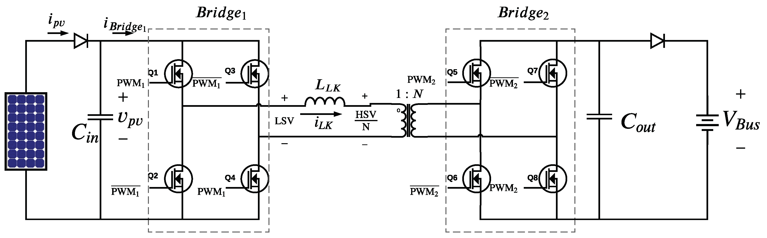
The electrical scheme of a PV system, based on the DAB converter, is presented in
Figure 1. The DAB converter is formed by two H-bridges with four active switches, each bridge (
and
) can operate as rectifier or inverter depending on the power flow direction. This dc/dc converter also has a high frequency transformer (HFT) connected between the ac side of both bridges to transfer the energy from one side to the other. The HFT turns ratio
is selected according to the requirements of increasing, decreasing, keeping equal the voltage at the input and output ports. The leakage inductance
must be selected depending on the maximum power provided by the PV module as it is reported in [
20]. In addition, the input capacitor
and the output capacitor
are necessary to absorb the high frequency currents caused by the switching in both bridges [
21]. In PV applications must be avoided the DAB bidirectionality, otherwise the PV panel could be heated by currents flowing from the dc/dc converter, which reduce the panel lifetime [
22]. Therefore, the PV system in
Figure 1 considers two diodes added at both the input and output ports of the converter. Moreover, the output of the DAB converter is connected to a dc bus absorbing the energy produced by the PV module, which is regulated by the second stage of a microinverter (a controlled inverter) to exhibit a regulated dc voltage
. This output condition is also present in microgrids, where a bus-regulator converter is used to ensure a safe bus voltage [
23].
The bridge on the left side of
Figure 1, named
, has a
PWM signal (
) to drive two of the four switches (
and
). If all the switches were triggered with the same
signal, a short circuit would result. To avoid this situation, it is necessary to obtain the complementary signal of the
PWM (
) to properly trigger the switches of
. Therefore, the
signal drives switches
and
, while
drives
and
, thus each
PWM (
and
) of
drives a diagonal of switches to invert the dc signal coming from the PV module. Similarly, on the active bridge two (
), another
PWM signal (
) triggers diagonal switches
and
, while the complementary
signal (
) triggers the diagonal
and
to rectify the signal previously inverted by active
. Therefore, both bridges are controlled by two
PWM signals (
and
) and each one has a complementary signal (
and
) to control a total of eight switches. Between
and
there is a triggering relationship, since the
changes the state some time after
; this time delay is also measured in terms of the angle between the
PWM signals and it is known as phase shift, it being represented as the angle phase shift
[
24].
The phase shift factor
can change from
to 1: for positive
the energy flows from the panel side to the dc bus, and for negative
it flows in the opposite direction. However, the highest efficiency of the converter is achieved for
values between
and
as it was demonstrated in [
20]. The power flow in the DAB converter depends on the value of
[
20,
25,
26,
27], thus such a variable must be controlled in order to regulate the dynamic behavior of a PV system based on the DAB converter.
Figure 2 shows the low side voltage (LSV) and high side voltage
waveforms, which corresponds to the voltages of active
and
, respectively, referred to the primary side of the HFT;
Figure 2 also reports the waveforms of the leakage inductor voltage (
) and current (
). It is important to note that the changes in the slope of the current waveform are caused by the phase shift (
) between the waveforms of the voltages
, thus it is a suitable control signal. Within a single switching period of those signals, the following four states occur:
State 1: LSV positive and negative, thus the slope of the current is positive. This happens before the phase shift between active and is reached.
State 2: LSV positive and positive, thus the slope of the current is positive but now in a smaller proportion to the previous state, this is because the difference between voltages is now much smaller. This state occurs when the phase shift between the active and has already occurred.
State 3: LSV negative and positive, thus the slope of the current is negative, mainly because the whole system is referred to the primary side of the transformer, therefore the difference between LSV (−) and (+) results in a larger negative value.
State 4: LSV negative and negative, thus the slope of the current is negative but in a smaller proportion. This is again due to the system referred to the primary side of the transformer, for this stage both magnitudes are negative; therefore, the difference between LSV(−) and (−) results in a much smaller negative value than the previous stage.
3. Model of the PV System
This section describes the proposed model, which is based on the Fourier analysis technique, hence the Kirchhoff voltage law (KVL) is applied to the loop formed by
,
and
in the circuit given in
Figure 1. Thus, assuming no losses in the transistors and inductor
, the Equation (
1) is obtained. In such an expression
is the leakage inductance,
is the panel voltage,
and
are the switching functions related to
and
, respectively. Moreover,
is the dc bus voltage at the output of the converter and
N is the turn ratio of the transformer.
In the same way, applying the Kirchhoff current law (KCL) at the upper node of
, the Equation (
2) is obtained, where
is the input current of the active
shown in (
3). In those expressions
is the input capacitance connected in parallel with the PV module,
is the short circuit current of the PV module, and
is the Norton model resistance of the PV module calculated as given in [
28].
Since
is the variable controlling the behavior of the DAB converter, the model Equations (
1) and (
2) must be transformed to explicitly exhibit this variable. Then, the next step is to apply the time derivative of the Fourier coefficients [
29] of those equations, which decompose the time-dependent signals into mean and harmonic values:
In expression (
4) each Fourier coefficient is represented using 〈 〉,
is the time derivate of the
nth Fourier coefficient,
j is the direction of the imaginary axis,
is the
nth Fourier coefficient,
is the angular frequency defined as
where
is the period of the function.
Then applying the Fourier analysis to Equations (
1) and (
2) leads to:
It is important to remark the difference between n and N; n refers to the Fourier harmonic number, while N is the turn ratio of the HFT (1:N). The terms , , , , and N are parameters or constant values; therefore, those are not decomposed in Fourier coefficients.
The proposed model is based on a representation accounting only for the fundamental and average component of each signal, i.e.,
. Including more Fourier coefficients could produce a more accurate model, but the model complexity will be significantly increased, which will difficult the model use for controllers design. However, the work reported in [
18] confirms that the average and fundamental component are enough to develop an efficient controller, this taking into account that those components are dominant. Therefore, to provide an acceptable model accuracy,
,
and
are taken into account.
The following subsections analyze both current (
5) and voltage (
6) differential equations.
3.1. Analysis of Differential Equation
The average value of
is zero since each bridge has a fixed duty equal to
in order to avoid an average current different from zero in the HFT, which increase the system losses [
9,
20]. Therefore, the average value of
, and only the components
and
are considered:
The next step is to find the product of two Fourier coefficients, which is needed to calculate the terms
,
,
and
of (
7) and (
8). However, the signals
and
must be first represented using the complex Fourier decomposition, such definitions are shown in (
9) and (
10), where
represents the complex Fourier coefficient formed by the real part
and the imaginary part
as shown in (
11); it should be noted that the complex Fourier coefficients with negative
n (
for this model), i.e.,
, are the complex conjugates of their positive counterparts as shown in (
11), where
is the conjugate operator.
To apply the procedure given in (
10), it is necessary to define the intervals for the functions
and
as given in (
12) and (
13), respectively. Those definitions are based on the switching behavior of the
and
, respectively, reported in
Figure 2.
The coefficients for
, calculated using expression (
10), are:
Solving the previous integral, considering that
, leads to:
Taking into account that
, Equation (
15) is simplified as follows:
Finally, the coefficient of
of
is given in (
17).
Similarly,
is analyzed by applying procedure (
10) to equation (
13):
Then, solving the previous integral leads to the Fourier coefficient for
given in (
19). Finally, the coefficient of
for
is given in (
20).
The product of the two Fourier coefficients is calculated as given in (
21) [
18], where
and
are the Fourier coefficients obtained from (
10), and
k is the
expansion of the summation.
Then, the product of two Fourier coefficients required to calculate (
7) and (
8) are obtained, starting with
and
:
Since the PV panel is a dc source, for a well-designed PV system the dc value of
is much higher than the harmonic components, therefore only the dc value is considered, i.e.,
. In contrast,
is the square waveform of a
PWM signal, thus it has a zero average value, and only the first harmonic (
and
) is taken into account. Under the light of the previous considerations, Equations (
22) and (
23) are simplified as follows:
A similar analysis is carried out for
and
. Replacing those coefficient products into Equations (
7) and (
8) leads to the following differential equations:
The Fourier representation for
and
must be further simplified by taking into account the Euler identity for an exponential complex number
, which transforms the
term (
20) into:
Then, the coefficient values of
and
given in (
17) and (
28), are replaced into Equations (
26) and (
27), as follows:
In a PV system, the output voltage (
) at the dc bus is constant, thus the term
is considered constant. Under the light of the previous consideration, Equations (
29) and (
30) are simplified and organized into real and imaginary parts:
Based on Equation (
11), the terms
and
are defined in (
33). Then, those expressions are replaced into Equations (
31) and (
32) to obtain (
34), where
is the real component of the harmonics
and
, while
is the imaginary component of the harmonics
and
.
Extracting the real and imaginary parts from (
34) leads to Equations (
35) and (
36), which represent the dynamic behavior of the real and imaginary coefficients of the first harmonic of
.
The time expression of the first harmonic of
, i.e
, is obtained by evaluating Equation (
9) for
, where the result is shown in expression(
37).
Replacing
and
into Equation (
37) leads to the trigonometric form of
reported in (
38).
3.2. Analysis of Differential Equation
A similar analysis is performed for the differential equation of the PV voltage
given in (
6). Since the PV module is a dc source, the voltage of the capacitor
is a dc value, hence the analysis of this differential equation only takes into account the average value (
) of the Fourier coefficient:
To determine the components of the product
it is necessary to expand such a term into the real and imaginary parts of both the dc and the first harmonic components, using the Equation (
21), as follows:
Taking into account that
and
terms are equal to zero due to their null dc components, and considering that the real term of
is zero as shown (
17), Equation (
40) becomes:
Finally, replacing the previous value (
41) into (
39) provides the differential equation for the PV voltage:
3.3. Analysis of the Current in Active Bridge One
The analysis of the current in active
, given in Equation (
3), is performed using the product value for
reported in Equation (
41), as follows:
Applying the charge balance at the input capacitor
of
Figure 1 confirms that the average current of the active
is equal to the average current of the PV module:
Therefore, it is possible to regulate the PV current by controlling .
3.4. Closed Form of the Non-Linear Model
In order to provide a closed form of the proposed non-linear model for a PV system based on the DAB converter, Equations (
35), (
36), (
42) and (
43) are expressed in matrix form as follows:
Since the model is based on the first harmonic components, this non-linear model is named the First-Harmonic-Approximation (FHA) model of a PV system based on the DAB converter. This FHA model can be used to design non-linear controllers such as sliding-mode regulators [
30] and adaptive voltage controllers [
31].
3.5. Linearized FHA Model
The proposed non-linear FHA model is useful to design non-linear control systems, but classical linear regulators, such as
PID or lead-lag controllers, require a linear model of the PV system. Therefore, this subsection proposes a linearized version of the model aimed at designing classical controllers. Such a linearization is based on the concept of small-signal average approximation, which leads to Equations (
47)–(
50), where the small-signal variables are
,
,
and
; the large-signal variables are denoted in lower case, i.e.,
,
,
and
; and the steady-state values are denoted in upper case, i.e.,
,
,
and
.
The first step is to replace Equations (
47)–(
49) into Equation (
35) as follows:
The presence of trigonometric functions makes difficult the treatment of the control variable
; thus, the trigonometric functions are approximated using the expressions given in [
19]:
Using the previous approximations, Equation (
51) is simplified as follows:
The linearization process is performed around the operating point determined by the variables
,
,
and
; therefore, the small-signal linearized equation, representing the dynamic behavior of
, is:
The same process is performed to Equation (
36), obtaining the expression given in (
56), which is simplified using (
53) as given in Equation (
57); such an expression only considers the small-signal variables.
Finally, the same procedure is applied to the non-linear differential Equation (
42), using the small-signal approximation (
50) as given in (
58). Finally, the small-signal equation is presented in (
59).
Then, the small-signal Equations (
55), (
57) and (
59) are concentrated into the matrix representation given in (
60), where the input variable of the model is the small-signal change
on the phase-shift signal.
The output equation, presented in (
61), provides the linearized values of both the PV voltage and the average current of the active bridge (
43), which is equal to the PV current as shown in (
44).
Finally, the linearized small-signal model of the PV system, based on the DAB converter, is given by expressions (
60) and (
61). From such a model is possible to obtain the transfer function
between
and
:
Similarly, the transfer function
between
and
is reported below:
Both and can be used to design classical linear controllers for the PV system.
4. Results and Discussion
The non-linear model and the linearized model are tested using the parameters given in
Table 1. Those values correspond to a PV system, based on a DAB converter, designed to extract the maximum power of a PV module BP585 [
32]; the design of such a PV system is reported in [
20]. The parameters reported in
Table 1 correspond to the maximum power point (MPP) of the BP585 operating at an irradiance equal to
. The switching frequency of the converter is 50 kHz, which corresponds to an angular frequency
= 100,000 rad/s.
The validation of the proposed model is performed by contrasting the model prediction with a detailed circuital simulation of the PV system carried out in the power electronics simulator PSIM.
Figure 3 shows the PSIM circuital scheme of the PV system based on the DAB converter, where the circuital model of the PV module is the configured with two signals: first, the irradiance signal (
S) is defined by a piecewise source, which is programmed to simulate changes on the irradiance conditions; the second signal is the ambient temperature (
T), which is defined with a dc source. The circuit includes the input diode to prevent current flows from the DAB converter to the panel, and two current sensors are placed near the diode; the first sensor measures the PV current, which is needed to track the MPP; the second sensor measures the input current of the
, which is used to verify the model performance. The first active bridge is controlled with the
PWM signal
and its complement
, and the second active bridge is controlled with the
PWM signal
and its complement
. Finally, the dc bus is simulated with a voltage source, which represents a bus capacitor with regulated voltage; such a dc bus is protected with an output diode to avoid power flows form the bus to the PV system.
Figure 3 also reports the phase shift circuit, which is formed by comparator, a sawtooth signal at twice the switching frequency, and the desired phase-shift value
. This circuit produces a clock signal
, which is in charge of updating the
PWM signals of the second bridge (
and
), introducing in this way the desired phase shift between the
PWM signals of both bridges. The figure also depicts the
PWM generator, which is based on the classical
PWM circuit for the first bridge (signals
and
). The
PWM signals of the second bridge are a delayed version of the
PWM signals of the first bridge; such a delay, given by
, is achieved by using a D-flip-flop controlled by the
signal. Therefore, changing the value of
introduces a phase shift of
between the
PWM signals of both bridges. Finally, both
PWM signals have a duty cycle of
, since such a value produces the most efficient operation of the DAB converter; such an optimal condition was demonstrated in [
20].
Figure 4 shows a comparison between the proposed non-linear equations and the PSIM circuital simulation, where the dynamic variables under evaluation are
, modeled by (
1);
, modeled by (
2); and
, modeled by (
3). The simulation evaluates both steady-state and dynamic behaviors: the PV system operates in steady-state up to 100 ms, which reports a coincidence between the equations and circuit signals; then at 100 ms, a perturbation in
(
) is introduced to force a dynamic behavior into the PV system. The simulation confirms a correct prediction of the leakage inductor current, which is also achieved in the case of the first active bridge current. The prediction of the dynamic behavior of
is also satisfactory, but the PV voltage exhibits a small steady-state error (1.28%) after the perturbation, which is mainly caused by the fact that Equation (
2) uses a Norton model, parameterized in a particular operating condition, to represent the PV module, while the PSIM circuit uses a much more complex and non-linear model of the PV module. In any case, the accurate prediction of the dynamic behavior of the PV voltage is evident, and an error of 1.28% in the prediction of the PV voltage is similar to the errors introduced by practical measurement systems [
33]. Moreover, the Norton model of the PV system could be parameterized for the new steady-state condition.
The next validation concerns the proposed non-linear FHA model, which is aimed at predicting the first harmonic and average values of the PV system variables. Therefore,
Figure 5 shows the simulation of
,
and
for a
perturbation at 100 ms, where the FHA model accurately predicts the first harmonic of the PSIM circuital simulation. For example, the prediction of
, constrained at the first harmonic, corresponds to a sinusoidal waveform with the same frequency of the square-like circuital waveform. Instead, the prediction of
provides the average current value of active bridge one with high accuracy; thus, the FHA model reproduces the dynamic behavior of the average values calculated within the switching period. Finally, the prediction of the PV voltage
exhibits the same dynamic behavior and settling time, but with a small error in the steady-state values (2%), which again, is produced by the Norton model used to represent the PV module in a particular operation condition. Therefore, this time-domain simulation confirms the accuracy of the FHA model, which can be used to design non-linear controllers.
Despite the satisfactory results of the time-domain simulation, a frequency analysis is needed to ensure the correct behavior of the model. In fact, several control-design techniques are based on the system frequency response, e.g., the linear active disturbance rejection controller (LADRC) [
34] and the fast PD control based on bode diagrams for dc/dc converters [
35], thus the model must to provide an accurate reproduction of the system frequency characteristics. This is evaluated in
Figure 6, where the Bode diagram for
produced by the FHA model and the PSIM circuit are observed. Such a simulation reports a small gain difference at low frequency, and a larger difference at high-frequency; this is because the model considers the average of the first harmonic. However, the dynamic behavior of the model follows closely the circuit, thus it is suitable for design control strategies.
Similarly,
Figure 7 reports the Bode diagram for
produced by both the FHA model and the PSIM circuit. In such a frequency analysis it is observed a small error at low frequency, which is caused by the Norton model used to represent the PV module. However, at higher frequency the FHA satisfactorily reproduces the dynamic behavior of the system, thus it can be used for control design.
Finally, the linearized FHA model must be also tested.
Figure 8 shows the time-domain prediction of
and
, provided by the linearized FHA model, contrasted with the PSIM circuital simulations. The linear model accurately predicts the average values of
, where the dynamic behavior caused by a
perturbation is also reproduced. Similarly, the linear model reproduces the dynamic behavior of the PV voltage after the perturbation, but exhibiting a small error (2%) in the steady-state values, which can be reduced by adjusting the Norton model parameters of the panel at the particular operating point. Therefore, the linear model can be used to design controllers based on time-domain techniques like the state-space based controller for a dc/dc converter reported in [
36], or to design controllers based on transfer functions like the one reported in [
37].
Similar to the non-linear model, this linearized model must be also tested in the frequency domain.
Figure 9 shows the performance of the model using the Bode plot for
, which exhibits a small difference in comparison with the PSIM circuit. Such a difference is attributed to the approximation of the model, which only considers the fundamental components. Nevertheless, it is possible to design linear control strategies based on this approximated frequency response.
Figure 10 shows the Bode diagram of
for the linear model, the non-linear model and the PSIM circuital simulation. It is noted some errors at low-frequency caused by the simplified Norton model used to represent the PV module, while at high frequency the linear model provides a satisfactory reproduction of the PV system dynamics. Therefore, the linearized model can be used to design linear controllers using frequency-based techniques.
In conclusion, the time-domain and frequency-domain comparisons presented in this section confirm the model accuracy. Therefore, such a model must be a suitable option to design model-based control systems; this characteristic is tested in the following section.
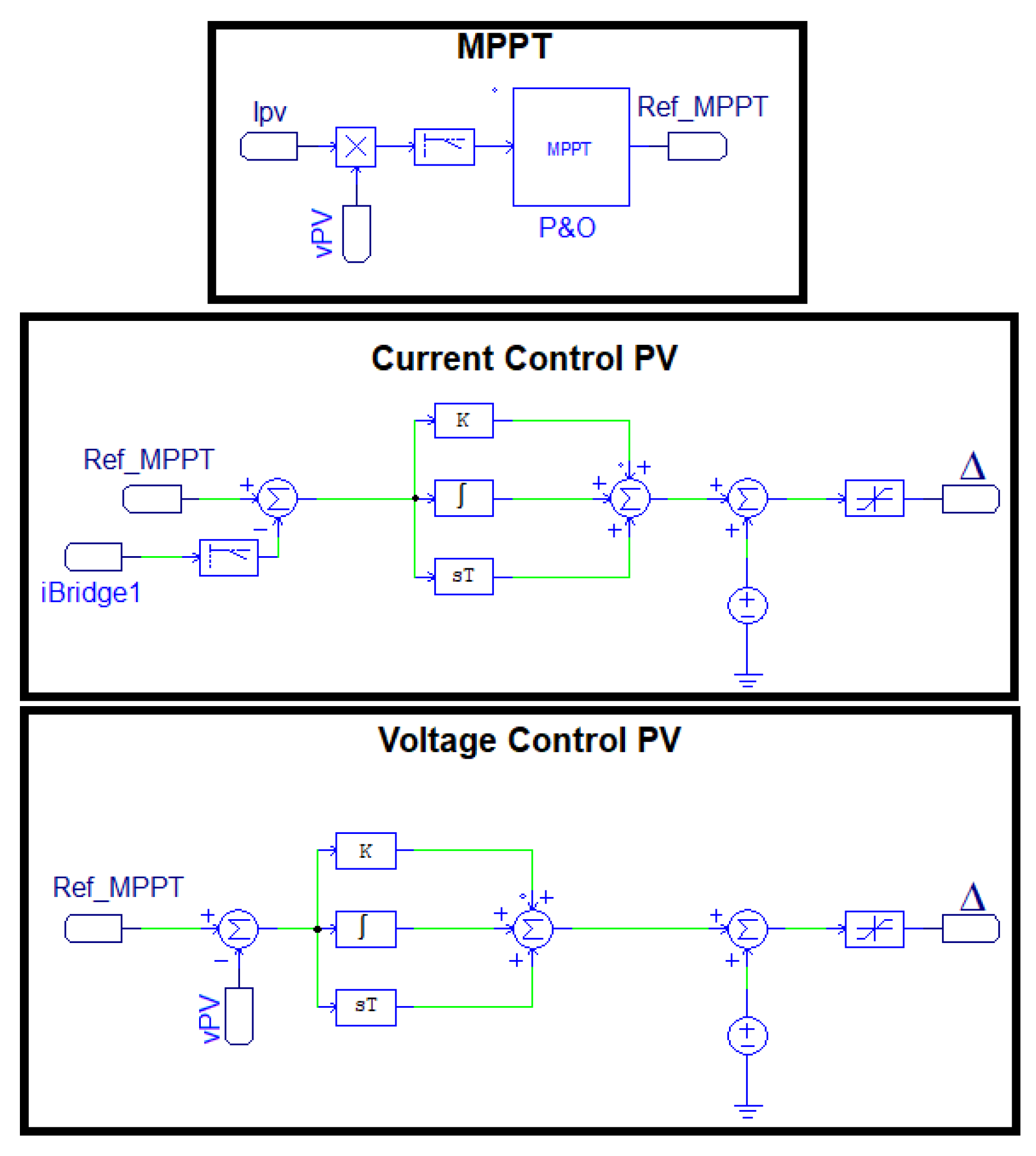
5. Application Example
This section illustrates the use of the proposed linearized model in the design of classical controllers for a PV system based on a DAB converter. Two control systems are designed in this section: an MPPT application based on the control of the PV current, and an MPPT application based on the control of the PV voltage.
Figure 11 shows the diagrams of the control blocks used to implement the two control systems. The
MPPT block corresponds to the
MPPT algorithm, where the input is the power produced by the PV system, which is filtered to remove the switching components using a low-pass filter with a cutoff frequency of 1 kHz [
38]. The output of this block (
) corresponds to the reference for the classical control system;
for the current controller and
for the voltage controller. The current control
block diagram corresponds to the first application, where
is regulated. In this case the
is filtered to obtain the mean value, which is regulated using a classical feedback-loop with a
PID controller; the objective of this controller is to ensure
to ensure the panel operation at the maximum power point.
The design of the
PID controller was performed using the Pole placement technique [
39], which requires the transfer function (
63) parameterized using
Table 1:
The
PID controller was designed with a damping factor of
and a closed-loop bandwidth of 30 kHz, obtaining the following controller:
The
MPPT algorithm adopted in this section is a Perturb and Observe (P&O) considering
ms (perturbation period) and
A (perturbation size) following the procedure reported in [
40]. This algorithm provides the optimal reference
for the
PID controller, which ensures the extraction of the maximum power from the PV system. Finally, the complete control system is connected as follows: The
MPPT block of
Figure 11 measure the PV current and voltage to calculate the PV power, and such a block provides the optimal reference
. That reference value
is provided to the current control
block diagram of
Figure 11, which also measures the
current to calculate the error. Such an error is processed by the
PID controller
to generate the small-signal change on the phase shift value
. Finally, the small-signal change is added to the steady-state value of the phase shift (using an adder) to generate the effective phase shift value
, and that value is provided to the Phase shift block in the scheme of
Figure 3.
Figure 12 reports the results obtained from the simulation. The first plot corresponds to
, depicting a non-saturated, smooth and stable response of the converter to the
reference. The second plot depicts
, which follows the reference imposed by the
MPPT block (
) reaching a steady-state after every change in the reference. This simulation, considers a 20% peak-to-peak perturbation at the bus voltage
(±22 V), which are depicted in the third plot; those three perturbations are satisfactorily compensated by the current controller designed with the proposed model. The PV voltage
is also observed, which is always regulated within [17.5–18.5] V because controlled PV current ensures a stable operation of the PV system. The last plot shows the maximum possible PV power and the power harvested with the DAB converter, which confirms the operation of the PV system close to the MPP even in presence of perturbations in
.
The second example is based on regulating the PV voltage using a
PID controller and the
MPPT algorithm. The design of the
PID controller is also performed using the pole-placement technique, but in this case the design was based on the transfer function given in (
62) parameterized using the values given in
Table 1:
The voltage
PID controller was designed to provide a damping factor of
and a closed-loop bandwidth of 30 kHz:
The voltage regulation scheme, also depicted in
Figure 11, is the following one: the P&O algorithm defines the optimal reference
to the voltage controller; such a
MPPT controller was designed using the procedure reported in [
40], obtaining the P&O parameters
ms (perturbation period) and
V (perturbation size). The voltage reference
is now provided to the block diagram (6) to calculate the voltage error using a subtracted, and such an error is processed by the
controller to generate the small-signal change on the phase shift value
. Finally, that small-signal change is added to the steady-state value of the phase shift (using an adder) to generate the effective phase shift value
, and that value is provided to the Phase shift block (2) in the scheme of
Figure 3.
Figure 13 reports the simulation results of the
MPPT application based on the voltage controller. The first plot shows the control action
, which confirms the stability of the
PID controller designed with the proposed linearized model. In such a simulation,
exhibits a smooth and non-saturated value, thus the system operates by following the reference provided by the
MPPT algorithm. This is further observed in the
waveform, which is always equal to the
MPPT reference
. Moreover, the simulation shows a null steady-state error in the PV voltage, which is achieved due to the integral action of the
PID controller. The waveforms at the bottom report the harvested PV power and the theoretical maximum power achievable. Such a simulation confirms the correct operation of both the
MPPT algorithm and the
PID controller, since the PV module is always operating around the MPP, even under different irradiance conditions.
In fact, the simulation considers three changes on the irradiance: first, the irradiance starts at
, where the PV voltage exhibits the stable three-point profile of the P&O algorithm [
40]. Then, the irradiance changes to
, and the
PID controller changes
to ensure a correct tracking of
. Another change is performed in the irradiance, reaching again
, Finally, the irradiance is further increased to
. In all cases the PV system operates as predicted: the P&O algorithm changes
to force the PV system to produce the maximum available power, while the
PID controller changes
to force the DAB converter to follow the reference. This iterative action is observed in the Power vs. Voltage curves at the bottom of
Figure 13, where the PV system (blue trace) always operates around the maximum power of each curve, i.e., for each irradiance condition.
In conclusion, the simulations presented in this section confirm the usability of the proposed model in the design of classical controllers for a PV system based on the DAB converter.
6. Conclusions
DAB converters have characteristics that are raising their use in several applications. Among their characteristics, high voltage-conversion-ratio and high efficiency make the DAB converter suitable to interface PV panels with electric grids. Therefore, an extensive mathematical model of a DAB converter connected to a PV module including protection diodes, an explicit linearized version of the model, and a detailed application example were presented in this work. The development of the models was focused in controlling a PV system, and the modeling approach was presented in detail to encourage the use of the model. Simulation results shown the close representation provided by the control-oriented model to the non-linear equations systems and the electric circuit, which are considered high detail models. Time and frequency domain simulations comparing bridge current, leakage inductance current and PV voltage confirms the close representation of the control-oriented model. Finally, the simulation of a realistic application validated the effectiveness of the model to design classical controllers for a PV system based on a DAB converter. Two control approaches were evaluated, an MPPT based on the control of the PV current, and an MPPT based on the control of the PV voltage.
For future work, the implementation of the PV system with its controllers will be done. Also, taking into account that microinverters connected to the electrical grid can be built with DAB converters, and the harmonics studies are essentials to connect devices to the electrical grid, it is necessary to extent the proposed modeling so that it includes the harmonics components. On the other hand, there is a field of research around modeling along with other renewable energy devices and advanced control strategies that can be implemented to further improve the effectiveness and versatility of the DAB converter. Furthermore, design a microgrid exclusively using the DAB converter for several renewable energy sources with distributed loads, in both dc and ac, is a promising future work to simplify energy management systems and improve the capacity and scope of microgrids along with their energy efficiency.


 ,
, 


