1. Introduction
The enhancement of the power electronics components in various applications of the renewable energy sector leads to the requirement of efficient components or configurations so as to obtain better results. Power electronics components play a vital role in transforming power supply and renewable energy resources-based applications [
1]. The selection of the accurate topology plays a vital role in building efficient configuration. The entire effectiveness of the solar photovoltaic (PV) system depends on the tracking of the Maximum Power Point Tracking (MPPT), selecting the efficient DC-DC boost converter, and implementation of the efficient configuration of the inverter with control strategies for the grid connected PV system. Significant work has been done in the field of MPPT for its various types and applications [
2,
3,
4,
5], its superior or improved versions with high accuracy, and fast-tracking under different environmental conditions [
6,
7,
8]. In [
9], a modified MPPT algorithm for reducing the inter harmonics present while tracking maximum power point is proposed whereas, a new concept called boost MPPT system is based on non-linear dynamics so as to track global MPPT without any additional external circuitry is provided in [
10].
Equally advanced work has been carried out by researchers on DC-DC boost converters. Some topologies with high efficiency, cost-effective, and high step-up are proposed in [
11,
12]. A comprehensive review of DC-DC converters topologies based on five major drives and accordingly classifying their area of applications is reported in [
13]. A comprehensive analysis of the DC-DC converters is provided in [
14,
15]. A novel high step-up DC-DC converter is provided in [
16]. A comparative study of diverse non-isolated DC-DC boost converters is provided [
17]. DC-AC converter or inverter topology is also the key factor for a photovoltaic system. In [
18], a review of the various inverter topologies or single-phase systems is provided. Specific investigations on inverter topologies have also been done by many researchers. Few of them include multilevel inverter topology [
19], transformer-less type inverter topology [
20], enhanced z-source [
21], and online variable topology [
22]. The paper [
23] provides the recent trends in inverter topologies. In [
24], the disturbance control strategy for LCL filter type grid-connected inverters is focused. The performance of the proposed control method was compared with other conventional control techniques for proving its effectiveness and stability. The matter of fact is that the advancement and researches done with respect to MPPT, DC-DC converters, and DC-AC converters are substantial and grooming with day-to-day advancement in technology. Researchers are focusing on cost-effective, efficient, reliable, and sustainable topology so as to get the most power at the least cost. However, issues pertaining to grid integration, like power quality, also need to be addressed for maintaining a stable and secure system. The power quality responses of grids under usual and unusual conditions with grid-connected solar water pumps have been analyzed [
25]. In the paper [
26], the power quality issues at the distribution grid after integration of roof-top solar PV system are presented. The recent developments in the grid-connected solar PV system are highlighted [
27]. A detailed review of the topologies available in the literature is provided [
28]. In the paper [
29], emphasis is given to the recent integration requirements related to power quality (PQ) issues. The paper also proposed the control for mitigating PQ concerns whereas the paper [
30] discussed the design of fuzzy based space vector PWM controller for mitigations of the power quality issues in the grid connected converters.After reviewing the existing research, some limitations were observed in the area of loss minimization on the DC side and ripple reduction at the DC link capacitor. Also, many researchers have used additional power control devices such as UPQC, DSTATCOM, etc., which enhance the additional cost of the system. Controlling the power on the DC side can enhance the conversion efficiency and thereby reduce the DC ripples present at the DC link capacitor.
The present paper emphasizes the efficient topology of the DC-DC converter so that the maximum power loss can be controlled and maximum efficiency can be obtained on the DC side with reduced ripples present at the input of the inverter. A synchronous interleaved boost converter was developed and presented in this paper. Efforts were made to develop the prototype in the laboratory and test it for the grid integrated solar PV system. Among the various intelligent controllers, the PSO based MPPT controller and the synchronous frame reference (SRF) based phased lock loop (PLL) control strategy for grid synchronization and control were used in this paper. The key objectives of this proposed configuration are as follows:
This proposed synchronous interleaved boost converter has a switch in place of the diode in the conventional method, which reduced the switching losses across the diode and thus making a more reliable system as compared to the conventional type of interleaved boost converter available.
This system topology is simple to implement and is capable of controlling power on both sides, that is, on the generation side as well as on the load side. On the generation side, the optimum power was tracked using PSO-based MPPT and then the DC link losses were reduced by using switches in place of diode whereas maintaining the power quality, power factor, and power management on the load side makes the system robust and practical.
In case of deviation in the load condition or deviation in the generation side due to solar irradiance, the proposed configuration coordinates with the power generation through the solar PV system and accordingly feeds continuous accessible power to the load to maintain the stability of the system. However, if any deficiency of power occurred from the solar PV system, the same shall be fulfilled by the existing grid power.
The response of grid and total harmonics distortion present in the grid after integration of the proposed system is also recorded in this paper.
The paper is organized as follows:
Section 1 describes the Introduction which includes proposed DC-DC boost converter and its advantages over the conventional type boost converter, system configuration and its hardware prototype.
Section 2 discusses the results obtained from the proposed system.
Section 3 concludes the paper. Authors contribution and references are mentioned thereafter in the paper.
1.1. Proposed DC-DC Boost Converter
The basic architecture of the grid integrated solar PV system has mainly three segments which are the DC side, AC side, and DC link as shown in
Figure 1. Onthe DC side, the main components are solar PV array and DC-DC converter with MPPT controller; the AC side includes the inverter, filter, and isolation transformer with the AC controller and decoupling capacitor or DC link capacitor, which acts as a link between the DC side and AC side.
The prime focus was given to the DC part of the architecture in this paper. Hence, emphasis was given to the MPPT controller for catering to the real-time variation and to the DC-DC converter for reducing losses and maintaining fewer ripples at the DC link capacitor so as to achieve better results on the AC side of the system.
The selection of topology and further choosing its hardware components required for implementing the same to design the DC-DC converter plays a significant part in formulating the dynamic system. The selection is based on various factors like voltage rating, on-state resistance, current flowing, and switching frequency. The culling of the switching device to be used in the DC-DC converter depends on the intercepting voltage, on-state resistance, and switching frequency. MOSFET and IGBT are the most prominent components used as a switching device. If the intercept voltage is below 700 V, then it is preferable to use MOSFET because it provides low conduction loss. Above 700 V voltage level, IGBT is the better choice. The IGBT based control switch was used in this paper.
1.2. Benefits of Interleave Boost Converter (IBC) over Traditional Boost Converter (TBC)
A traditional boost converter is one having one IGBT/MOSET switch, a diode, and an inductor placed in the manner shown in
Figure 2. The traditional boost converter has the voltage gain represented as:
where,
D stands for the duty ratio, and current across inductor
IL is given as:
At duty ratio,
D = 0.5, the current and voltage stress experienced by the diode and IGBT switch is within permissible limits whereas at a high value of duty ratio or high voltage gain, that is,
D > 0.7, the diode conducts for a prolonged time as compared to the desired value and thus causes an enormously high current and voltage stress [
31]. Also, the power loss afterward, over the diode, becomes steeply high at such duty ratios. Thus, photovoltaic applications having large voltage gain and involved in high power capabilities do not suit the use of the conventional type boost converter.
Interleaving the boost convert makes it the special type of boost converter where the current entering into the input gets divided into two paths so as to diminish the conduction losses and hence increases the effectiveness of the scheme.
Figure 3 illustrates the typical boost converter with the interleaved facility where the input current (
Io) is divided into two paths having current
IL1 and
IL2.
The value of the inductor also gets reduced. The expressions for IBC are:
where,
D is the duty ratio, and inductor current
IL is given as:
The proficient ripple frequency at the capacitor’s output also improved due to interleaving and thus reduces the ripple voltage conveniently at the converter’s output. Also, as compared to the CBC, the IBC is able to handle more power.
1.3. Synchronous and Non-Synchronous Means of Operation
The fundamental operation of the converter with traditional boosting capabilities and interleaving is usually based on the non-synchronous mode. In the non-synchronous mode of operation, the converter contains the combination of IGBT/MOSFET and diode. However, during the synchronous mode of operation, the diode is substituted by the switch, either IGBT or MOSFET, thereby reducing the losses, and hence the efficiency of the converter gets enhanced. The loss calculations of boost converter under synchronous and non-synchronous mode are analyzed [
32]. There are two sources of power loss across IGBT/MOSFET one is power loss across the resistive elements of the MOSFET and the second is the dissipation of power due to the switching losses. Further, the size of MOSFET is conversely proportional to the resistance loss. More is the size of the MOSFET, less will be the resistance loss. This resistance is called on-resistance (
Ron). The second loss is the switching loss. When MOSFET toggles on and off, the inherent freeloading capacitance accumulates and then disperses the energy at each interval. The switching frequency is directly proportional to this loss and thus with the enhancement in the size of the MOSFET, its capacitance also enhances resulting in enhancement of switching loss. The expression for the same is as below:
Power loss across IGBT/MOSFET:
where,
D stands for the duty ratio,
Ron represents the on-resistance of MOSFET,
f denotes the switching frequency,
Co represents the capacitance at the output of the MOSFET and
Po is the output power and power loss across the diode is given as:
where,
VF represents the forward voltage drop,
RF stands for the forward resistance of the dynamic diode and
Vo is the output voltage.
Loss across the inductor (
PL) and capacitor (
PC) is given as:
Therefore, as the synchronous mode of operation is adopted, the power loss across the diode as represented in Equation (6) gets replaced by the power loss across the MOSFET as represented in Equation (5) making the synchronous configuration more efficient.
1.4. Circuit Diagram of Synchronous Interleave Boost Converter
In the present paper, the boost converter with the interleaved facility is proposed, which is working in the synchronous mode of operation. This synchronous interleaved boost converter (SIBC) has a dual advantage, that is, the advantage of interleaving the input current thereby reducing the losses and second operating in the synchronous mode, that is, by replacing the diode with the IGBT/MOSFET. The circuit design of the prospective model is demonstrated in
Figure 4.
As observed from
Figure 4, the two IGBTs and the two diodes were replaced with the two MOSFETs/switches say S
1 and S
2. Due to interleaving the inductor L is divided into two parallel inductors having values L
dc1 and L
dc2. The output voltage (
Vo) and load current (
Io) was derived and is represented as:
where,
T is the total duration of time the converter is conducting and Δ
t is the incremental time of conduction.
1.5. System Configuration and Hardware Setup
The configuration of the synchronous boost converter-based grid connected solar PV system is shown in
Figure 5. The system consists of the 1.5 kW grid integrated solar PV system, a highly efficient synchronous interleaved boost converter having two shunt connected inductors having a value of 2.3 mH, input capacitance of 470 µF each, and output capacitance of 1200 µF. The diodes were replaced with the IGBT based switches, which are denoted as S
1 and S
2 respectively. The three-stack voltage source converter having three IGBTs branches containing two switch ports was connected with the boost converter with the DC link capacitance having a value of 1200 µF.
The technique used for tracking the maximum power point in the proposed configuration is particle swarm optimization (PSO), which is used to generate pulses and regulate the switches of the boost converter. The PSO was selected due to its faster response in case of the partial shading conditions of PV modules. The typical PSO method may be described using the following equations:
This algorithm is an intuitive method that is used for optimization by calculating the fitness function and then continuously amending the local best (LB) and global best (GB) points thus assuring the chasing of global maxima if the situation of partial shading conditions persists.
The AC side controller also plays a vital role in grid synchronism. The foremost requirement for grid synchronism is to measure the grid voltage (V
grid), phase angle (Φ), and frequency (f) and match with the voltage, phase angle, and frequency of the inverter output respectively. In this paper, the phase lock loop (PLL) based method has been used due to its advantage of well-established and simple configuration to implement. The synchronous reference frame phase lock loop (SRF-PLL) used for the control at the AC side is shown in
Figure 6. The SRF-PLL determines the phase and frequency of the grid voltage. The outputs of the SRF-PLL are the sine and cosine signals with unit magnitude. These are known as the unit vectors and are utilized to produce reference signals. The SRF-PLL is capable of handling disturbances like DC offset, unbalance, and harmonics.
The hardware prototype was developed wherein the control was provided with the help of a dSPACE DSP board 1104 [
33], which is used as an interface between the hardware components and the computer-based algorithms for control strategies. The complete hardware setup is illustrated in
Figure 7.
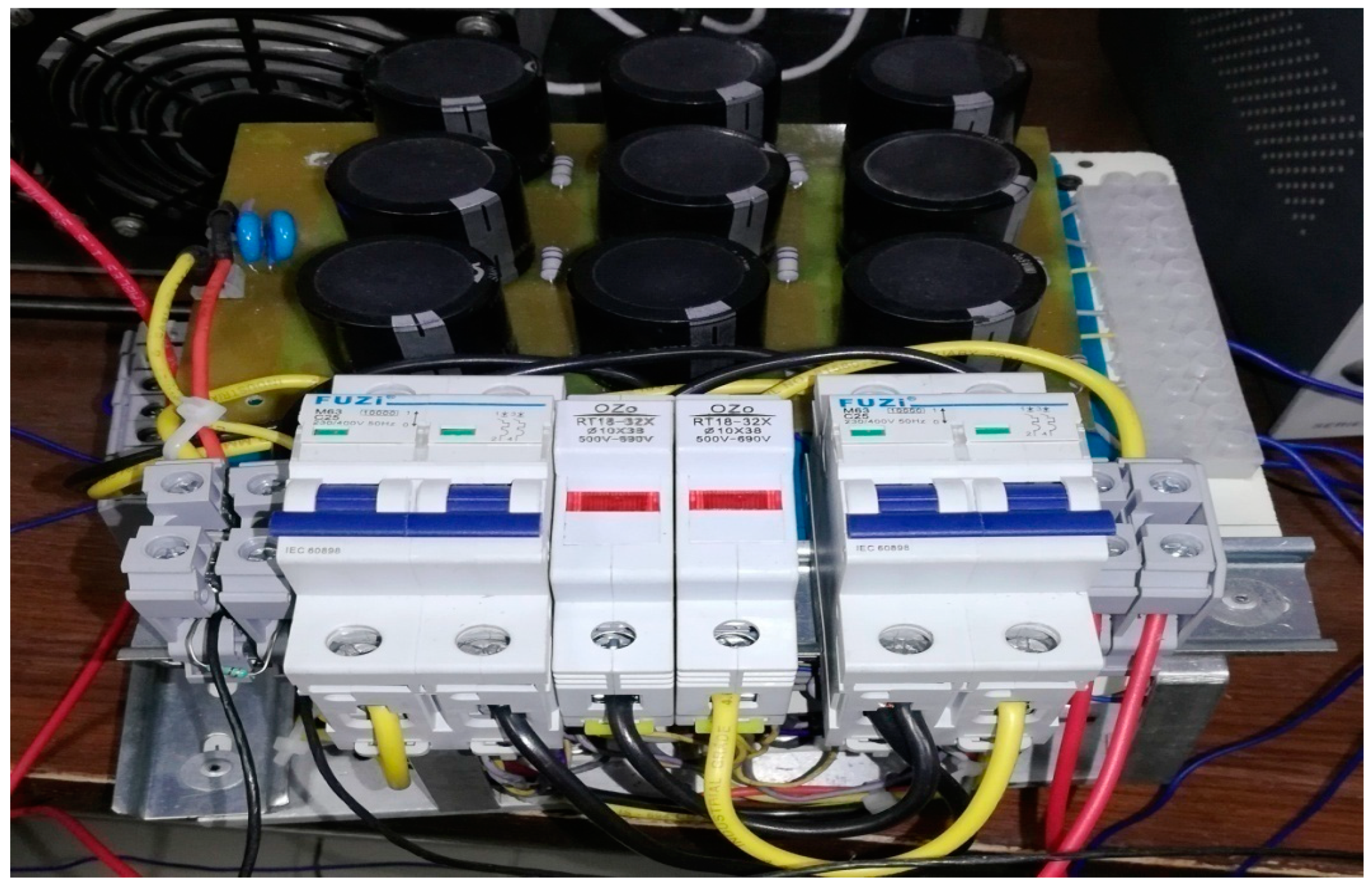
The hardware archetype of the synchronous interleaved boost converter was established after theoretical study and carrying out the simulation and the replica of the same is demonstrated in
Figure 8.
The hardware of the synchronous interleaved boost converter consists of the two-leg IGBT, DC link capacitor, input capacitor, HRC fuses for protection, and input inductor. The rating of the same is given in
Table 1.
For sensing the current and voltage of the PV system and the grid, the sensory circuit was designed. This sensory circuit shall sense the actual value of the current and voltage and feed to the computer-based controller through dSPACE 1104.
The current is sensed using the sensor, LEM LA 25 P and the voltage through the sensor, LEM LV 25 P.
The three-phase, 10 kVA, 415 V AC, 50 Hz, with a switching frequency capability of up to 20 kHz, three-stack voltage source converter was designed for the proposed configuration. The proposed voltage source converter can cater the DC voltage range from 200 V to 800 V. The Semikron make SKM100GB12T4 IGBT having a pair of switches was used as one leg and four such legs were configured, one for each phase R, Y, and B, and one leg spare for either grounding purposes or as a standby. The Semikron IGBT driver circuit was used for driving the IGBT. The hardware realization of the voltage source converter is shown in
Figure 9.
2. Results and Discussions
The 100 kWp solar PV system was designed and simulated with a solar PV module of rating 305 Wp each. A total of five modules were linked in sequence and 66 such strings were connected in shunt to form an array. A total of five modules were linked in sequence and 66 such strings were connected in a shunt to form an array. The variation of irradiance and temperature was considered under this study for vetting the response of the proposed system under different environmental uncertainties.
For analysis, the same, the 1.5 kW hardware archetype was established in the research lab. The DS1104 DSP board was based on a 64-bit PowerPC type PPC603e processor. The board included analog to digital (A/D), digital to analog (D/A) converters, and digital incremental encoder interfaces. The controller was designed using MATLAB Simulink and the pulses generated were provided to fire the IGBTs in the hardware setup using dSPACE Control Desk software [
33]. The controlling of the firing angle and other controls was done using dSPACE graphical user interface GUI software. With this GUI, it was possible to see the real-time output and any changes in the controller could be observed on a real-time basis. The pulses given to the IGBTs of the synchronous boost converter are shown in
Figure 10, whereas the 1.5 kW solar PV modules installed on a roof top were used for providing DC power to the proposed prototype, which is illustrated in
Figure 11.
The magnitude of irradiance considered was 1000 W/m
2 initially and it varied over the time period. The simulation was done for 2.5 s. At time t = 0.6 s, the irradiance varied to the level of 200 W/m
2 and then started rising to attain the value of 1000 W/m
2 at time t = 1.7 s. Then, to vet the variation of the temperature, the temperature was initially considered as 25 °C till t = 2 s. After 2 s, the temperature rose to 50 °C.
Figure 12 depicts the responses received from the photovoltaic system under different environmental conditions.
It was observed that as the irradiance value dipped, the corresponding voltage and power also dropped in the same respect, which shows the direct relationship between the irradiance and voltage. However, with the increase in temperature, the voltage and power reduced, which illustrates the inverse relationship between the temperature and voltage till the standard temperature condition (STC) of the PV module.
The synchronous interleaved boost converter configuration was implemented for this grid tied solar PV system. For verifying the reliability and robustness of the proposed system, a comparative analysis of the synchronous mode of operation and non-synchronous conventional type of boost converter was carried out. The simulation results obtained are shown in
Figure 13. The response in black color denotes the non-synchronous mode whereas the response obtained in magenta color is the proposed synchronous mode of operation. The response clearly depicts the stability and efficient regulation of the ripples of the output voltage waveform from the synchronous mode of operation as compared to the non-synchronous mode.
The simulation results illustrate the presence of fewer ripples in voltage for the DC link capacitor when functioning in the synchronous mode of operation and it is stabled in early time with stable voltage. Also, the average magnitude of the DC voltage measured is greater in the case of the synchronous mode of operation as compared to the non-synchronous boost converter. The voltage at the output of the voltage source converter is after the DC link capacitor was measured and is shown in
Figure 14.
It was observed that the conversion efficiency of the proposed converter configuration was recorded to be more than 93% under different duty ratios. To synchronize the output response received through voltage source converter with the power grid, the synchronous reference frame phase lock loop-based AC control scheme with PI controller was implemented. The complete AC control scheme is demonstrated in
Figure 15.
The sensory circuit senses the three-phase voltages (V
a, V
b, and V
c) and currents (I
a, I
b, and I
c) from the grid and fed into the control scheme. Then these three-phase voltage signals are converted into the two-phase stationary frame using abc to αβ transform using Equation (13).
Then these stationary frame values Vα and Vβ transform into the rotating reference frame. This conversion is called αβ to dq transformation. This is carried out using Equation (14).
where θ
e is the estimated angle calculated from the synchronous reference frame-based phase lock loop. The PI controller is used in association with the PLL so that the value of V
d is terminated or zero at steady state and the grid voltage is preferably aligned with the q-axis of the rotating reference frame. After the process of PLL, the outcome received is the estimated frequency, which is represented here as ω
e and estimated angle θ
e. This estimated angle is multiplied with the sine and cosine factor to generate unit vectors Sinθ
e and Cosθ
e respectively.
The system acts as nonlinear due to the rotating reference frame which is transformed from the stationary reference frame. The value of V
d is calculated using Equation (14) and is given as:
Differentiate Equation (15) with respect to θ
eThe estimated frequency is given by:
where,
Equation (19) is a nonlinear equation. Vα and Vβ are quadrature signals wherein Vβ lags 90° with respect to Vα.The Id_ref is generated by comparing the actual assessment of voltage at DC link (Vdc) and reference value Vdc_ref in DC link controller whereas Iq_ref is generated by evaluating the reference value reactive power in the grid using a Q controller based on the dips present in the grid and then this reference value is given to the inner current loop to generate the same.
Figure 16 displays the voltage and current profile at the output of the grid integrated solar PV inverter.
Figure 17 is the voltage and current profile of the grid where the voltage level at the grid side is considered at the primary distribution system, which is at 20 kV voltage level which can be stepped down with the help of a distributed transformer for further integration into the distribution side and consumer load.
The voltage and current at inverter output and point of common coupling of the distributed network was recorded using Fluke Energy and Power meter and is illustrated in
Figure 18 and
Figure 19 respectively.
It was observed from the
Figure 18 that the average magnitude of the output voltage at each phase of the inverter (V
i_abc) with respect to time is near to the value 240 V or line voltage of 415 V. Moreover the distortions at grid voltage (V
grid_abc) are more as compared to the inverter output voltage. To mitigate the difference in each phase voltage, an SRF-PLL based controller was used. Similarly, the response of rms phase current injected into the grid by voltage source converter and the grid current at each phase has was observed and is shown in
Figure 19.
During the observations of the behavior of the current waveform, it is seen that small ripples were present in the grid current. However, at certain fractions of a second, the current from the inverter becomes constant with no ripples or distortions. The role of SRF-PLL based controller used is to regulate the injected current into the grid so as to maintain the constant level of the current waveform.
It is significant to measure and analyze the power wave of the grid before injecting the inverter current into the grid or before grid connection. The power wave at each phase is to be observed so as to reduce the error difference between the grid voltages and inverter output voltage and thus making the phase match with each other. The same conditions are for each phase current of the grid and inverter.
Figure 20 shows the power wave of the grid depicting the general trends of variations of the waveform.
The graphical result shows an assessment of frequency, which is nearly sinusoidal in nature with a measured value of nearly 50 Hz. However, some difference was observed in the frequency of grid and inverter. The inverter frequency is nearly 50 Hz constant as presented in
Figure 21 whereas the frequency varies for the grid but it was observed that the frequency variations of the grid were well within the limit as per the IEEE 519 [
34].
Figure 22 shows the frequency spectrum at the point of common coupling (PCC) during the time span at a different number of events. Here, total 10 numbers of events were observed. It was observed that the frequency variation is from 50.03 Hz to 50.11 Hz out of which maximum times the value of frequency observed is f = 50.09 Hz, which compiles as per IEEE 519 standard.
The graph in
Figure 23 and
Figure 24 depicts the three-phase current and voltage analysis of the solar system and the grid side. It is seen from the figures that the waveform for solar system is pure sinusoidal whereas some notches has been observed at the tip point of the graphs as shown in
Figure 24.
Due to load variation at the grid, the voltage profile of the grid side varies and some distortions and notches at the edge points were observed. To compensate for these variations, IGBTs of the inverter/VSC were fired so as to mitigate the distortions. However, the grid voltage and current are always the references while calculating the compensation or error signals. If the grid fails, the reference point value stands at zero and hence, the inverter shall not get the power and go in islanding mode of operation.
The harmonic analysis of the grid side was also an important factor while the integration of the solar system takes place into the grid. For catering to the harmonics present in the grid, IEEE Std. 929-2000 [
35] has to be followed. The analysis of the harmonics on the grid side was observed and is shown in
Figure 25. It is seen that thethird, fifth, and seventh harmonics were present at each phase of the voltage. The 6n ± 1 harmonic is always present in the grid system, which can be viewed in the harmonics analysis of the grid. It can be seen in
Figure 25 that the harmonics present were approx. 3.4% which is less than the 5% THD and hence complies with the IEEE 519 standard.
The transients present in the network current travels in the distribution grid which is interconnected with the solar inverter. Hence, the current profile of the grid gets distorted, which is in general 120° out of phase with each other. This happens due to variation in the load side power demand As a whole, it can be concluded that the grid current and voltage have sinusoidal behavior, and the same is required if grid integration is to take place with a stable frequency. It is further noticed that if there is any deviation from normal operating conditions, like failure of the reference grid, the inverter isolates from the grid and stops injecting voltages into the grid.
The active power feed from the grid tied inverter after receiving from the solar PV plant through the DC-DC converter is shown in
Figure 26. It is observed that the power dipped at time t = 0.6 s and then resumed to the desired level at t = 1.6 s. This is due to the variation of irradiance at the generation side of the system. Also, at t = 2 s, a slight plunge was observed due to the variation in the temperature of the system at the input side. The results show that the power on the demand side varies as per the conditions on the generation side. The active power is directly proportional to the irradiance and hence a steep depletion was observed as recorded in
Figure 26 whereas, it is inversely proportional to the temperature so trivial moderation was traced during such a time period.


