Article

An Adaptive Switching Control Strategy under Heavy–Light Load for the Bidirectional LLC Considering Parasitic Capacitance

1
College of Information Science and Engineering, Northeastern University, Shenyang 110004, China
2
State Key Laboratory of Alternate Electrical Power System with Renewable Energy Sources, North China Electric Power University, Beijing 102206, China
*
Author to whom correspondence should be addressed.
Sustainability 2022, 14(19), 11832; https://doi.org/10.3390/su141911832
Submission received: 22 August 2022 / Revised: 14 September 2022 / Accepted: 16 September 2022 / Published: 20 September 2022
(This article belongs to the Topic Distributed Energy Systems and Resources)

Abstract

:
The LLC topology is widely used to link renewable energy and inverters to provide constant voltage in the smart grid. Due to its characteristics, the voltage regulation range under light load conditions is limited, so that the output voltage cannot be maintained constant. The adaptive switching control strategy is proposed in this paper to keep the output constant. Under heavy load conditions, the voltage is kept constant by adjusting the frequency to ensure the accuracy of the control. The phase shift is adjusted to achieve constant voltage, considering the influence of parasitic capacitance on the modeling process for the changing trend of output voltage in light load conditions. The switching point is calculated from the characteristic curve to ensure that the output voltage is stable during mode switching. In addition, there is a new hysteresis control which is robust near the switching point to cope with the instability of the new energy itself and frequent disturbance under light load. Finally, a 400V–36V–1KW prototype is used to verify this control strategy.

1. Introduction

With the development of the smart grid, renewable energy is used in forms integrated by the power electronic converters into the power system. The smart grid faces enormous opportunities and challenges, requiring a higher distribution network and converter requirements [1,2]. Inverters and DC–DC converters are used to connect renewable energy [3,4], such as photovoltaic, wind, and energy storage devices, to the grid [5,6,7].
Various electrical converters in the grid have been required to achieve high reliability, high frequency, high efficiency, high watt density, and low cost. The DC converters are divided into two types based on the transformer: isolated converters and nonisolated DC–DC converters. There are many DC–DC converters applying renewable energy. A method is proposed to reduce voltage ripple mixed with a neural network to provide a stable voltage for the latter inverter in constant power load conditions [8]. Compared with nonisolated converters, isolated conversion is suitable for a condition where the input and output differ significantly. Conventional isolated converters such as phase-shifted full-bridges have many shortcomings. The current ripple is diminished by changing the topology [9,10]. Dual active bridge (DAB) as a resonant converter is used when energy flows in both directions, in which two symmetrical H-bridges are on either side of the transformer. Ref. [11] adds switches to achieve soft-switch in the full range to reduce loss. The low efficiency is caused by the backflow power, and Extended Phase Shift (EPS) control is presented to reduce the backflow power [12]. Although there are various control methods, these are determined by their own topology and can only reduce the impact. Compared to DAB and other converters, LLC has lots of advantages, such as lower loss, lower current stress, and so on.
LLC can achieve soft-switching in the full range caused by the excitation in which the current flows through the switch before the voltage. The diodes are replaced with switches due to diodes resulting in a much needless loss in conventional LLC topology. There are many papers to research synchronous rectifiers (SR) [13,14], in which additional devices are needed to detect the current to add unnecessary loss. The pulse width locked loop is used to achieve SR [15]. The angle between the input voltage and the output current is used to control the conduction time of the MOSFET [16,17]. In addition, the switches are controlled by following the trajectory in which the current and voltage plots flow through the resonator [18]. These synchronous rectification methods are all digital control and only for the secondary side, which is complex in the program. A two-phase dual LLC resonant converter is adopted to widen the output voltage [19]. This topology changes rental with the different loads [20], which changes between the full bridge and half bridge. In [21], based on the new non-linear LLC model, a new observer is established but ignores the effects of parasitic parameters. Considering bidirectional energy flow, LLC has the DC bias in the reversed mode so that the output is less than the reference. Digital control for synchronous rectification is used in the reverse mode [22], which adopts different control methods, adding control variables instead of radically solving this problem. There are many control methods by digital [23]. The CLLC symmetry topology and a control method are valid for bidirectional flow in [24]. Meanwhile, ref. [25] adds an excitation inductor to solve the DC bias called L-LLC, and a new modulation method based on this new topology is presented [26]. Renewable energy is frequently disturbed under light load conditions. The converter needs strong robustness to maintain constant output voltage. In light load, the duty of the switches has been changed to keep the output constant in [27], and the effect of the excitation current is ignored, which causes some errors. The switch-controlled capacitor (SCC) is added to the topology to solve the load-sharing problem [28], adding additional switching losses. Refs. [29,30] avoid noise interference on the output in light load conditions, improving the efficiency in a wide range.
So, this paper proposes a new switching control method for LLC to keep the voltage constant in all regimes, especially under light load. The main innovations of this paper are as follows.
(1)
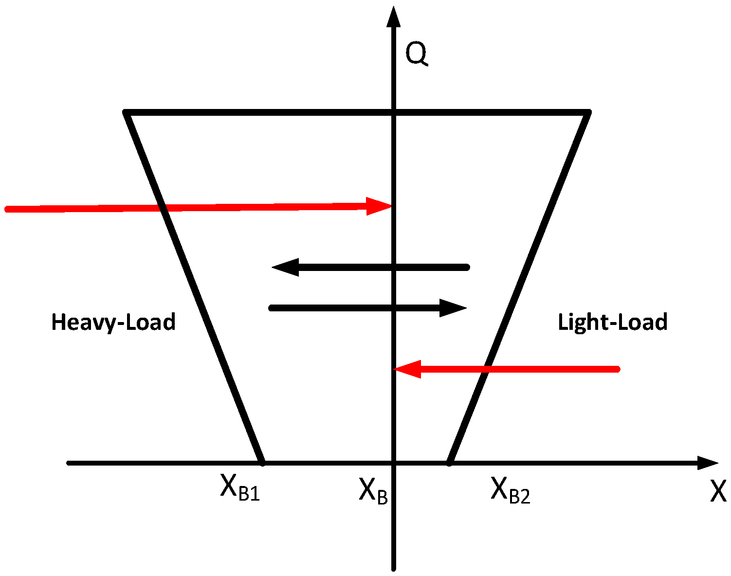
An adaptive switching control strategy is provided for the LLC, which can adjust the hysteresis loop boundary range according to the load. It solves the problem of higher output voltage than the reference and ensures the control continuity.
(2)
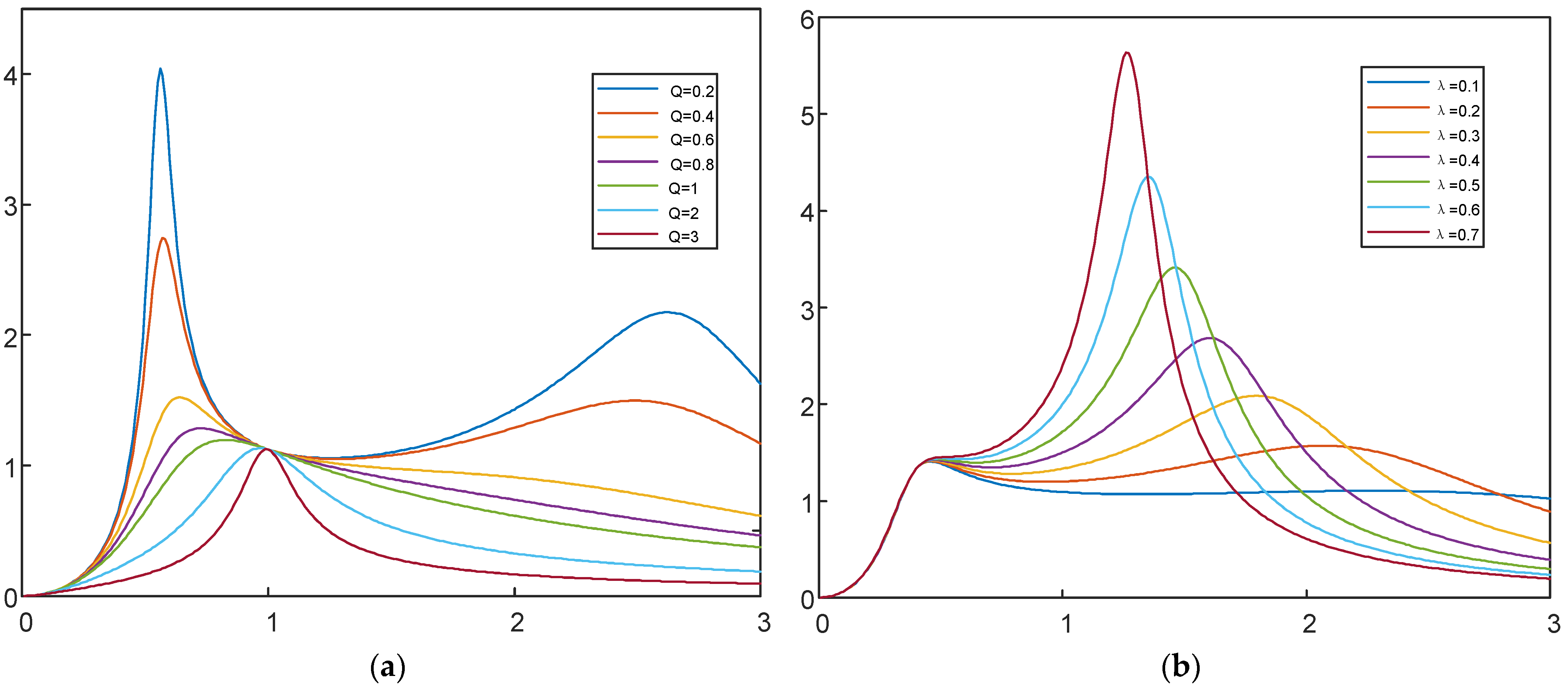
A bidirectional model considering parasitic capacitance is established, which compensates for accuracy in the light-load condition. It accurately describes the voltage gain curve under light load, which is more realistic than the previous model.
(3)
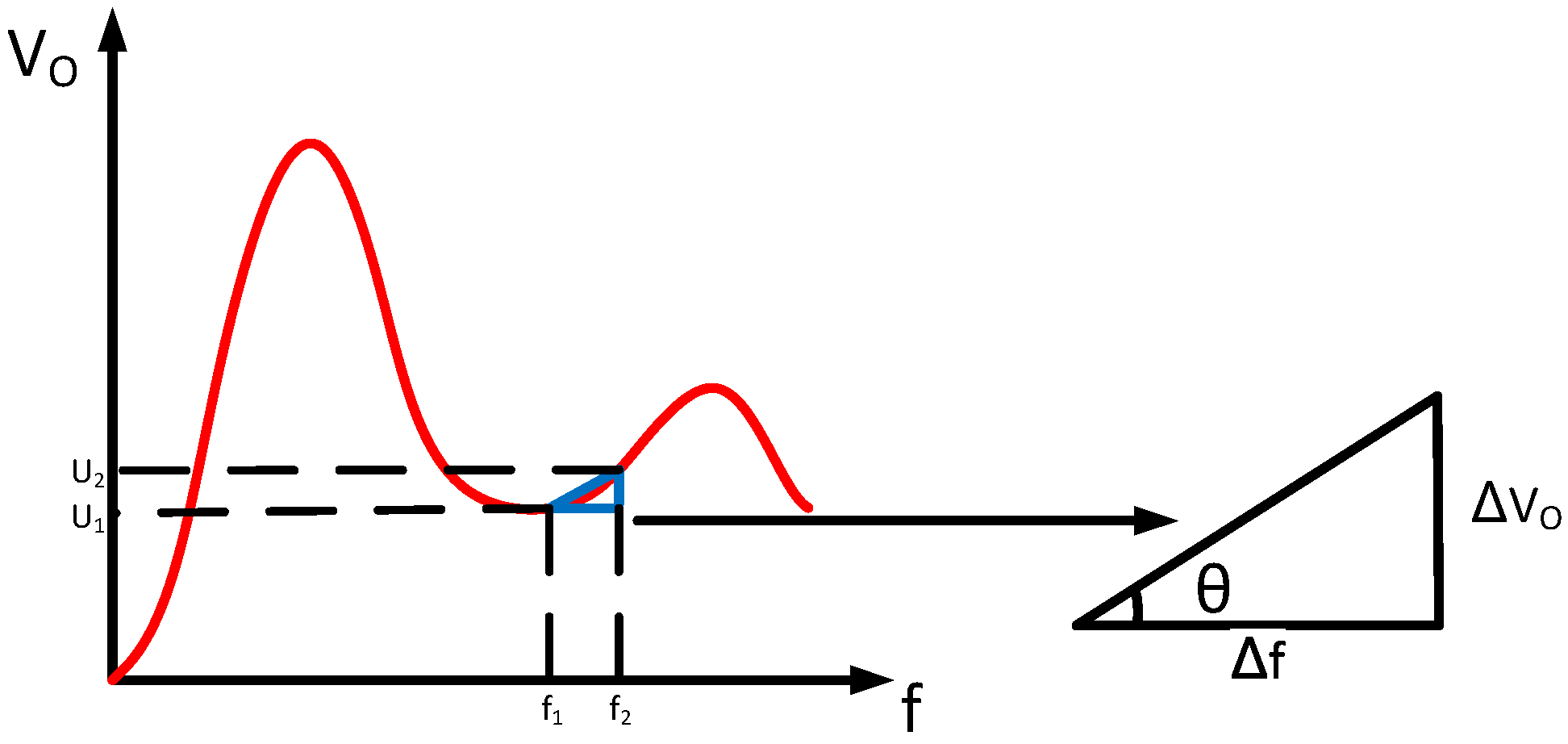
The mentioned switching points are determined according to the rate of change of the output voltage and frequency, which ensures smooth switching. In addition, the energy hysteresis strategy is adopted near the switching point, in which the length of the hysteresis adapts to load changes. It plays an important role in improving the stability near the switching point under slight disturbance.
The paper is organized as follows. Section 2 describes the conventional topology and its characters. The model with parasitic capacitance and the control method are discussed in Section 3, which improves the antijamming capability in the light-load situation and ensures that the output voltage is kept constant. In Section 4, a converter prototype and experiment are given.

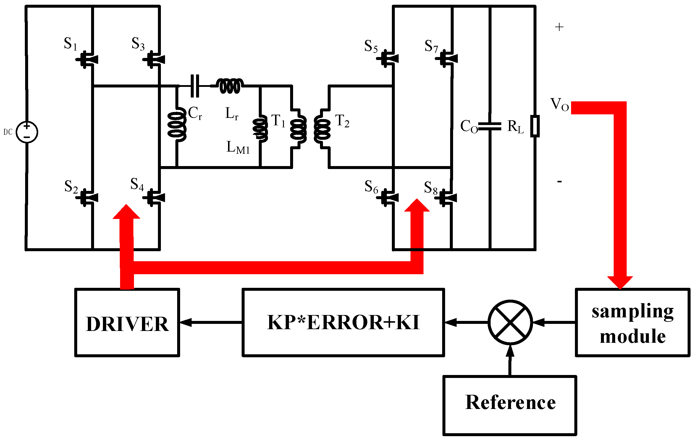
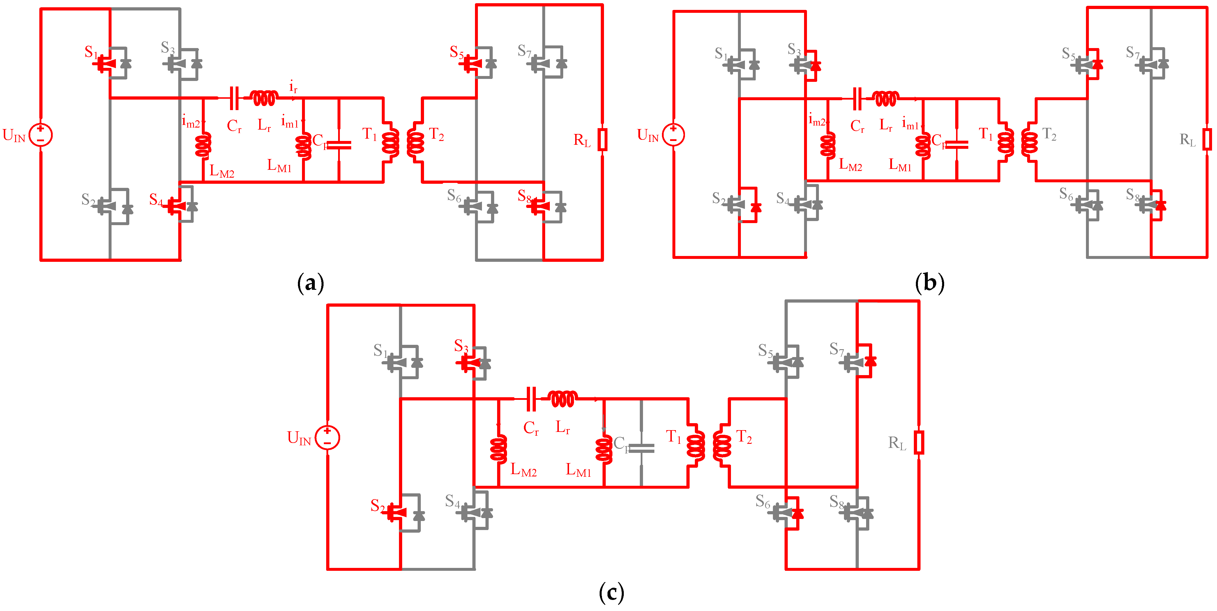
2. Conventional Topology and Control Method

This topology in Figure 1, which can solve the problem of voltage bias in the reverse mode presented in 2015, has three inductances: two excitation inductors, LM1 and LM2, and one resonant inductor, Lr. LM2 in the forward mode plays no role; instead, LM2 in the reversed mode act as the excitation. The whole circuit is symmetric if LM2 has the same value as LM1, which can eliminate the DC bias. The gain curve of the LLC is shown in Figure 2, which is similar to the conventional LLC circuit. When the switching frequency is below the resonant frequency, the gain of the curve is equal to (1), while the circuit voltage gain is equal to (2) when the switching frequency is beyond the resonant frequency. The output is influenced by Q, which means the quality factor deciding by the parameters of this circuit and load. Req is equal to the resistance of the rectifier circuit. In those equals, fs and fr are, respectively, the switching frequency and the resonance frequency.
G = 1 [ 1 + 1 k ( 1 1 x 2 ) ] 2 2 Q tan [ π ( 1 x 2 ) 2 ] ( x 1 x ) [ 1 + 1 k ( 1 1 x 2 ) ] + Q 2 1 [ cos π ( 1 x 2 ) 2 ] ( x 1 x ) 2
G = 1 [ 1 + 1 k ( 1 1 x 2 ) ] 2 + Q 2 ( x 1 x ) 2
where Q = L r C r R e q , x = f s f r , k = L M 1 L r . This circuit adopts PFM as the modulation method, which acts according to the gain curve. The switching frequency is modulated by the PI controller, as shown in Figure 3. After VO is sampled, the output voltage is subtracted from the reference value, and the error is controlled by PI. Compared with other controls, PI control does not introduce high-frequency oscillations and spikes. Other controls, while stable, can cause large current and voltage stresses that cause device damage. By calculating the value of switching frequency, the driving signal is issued to control [31,32]. S1 is complementary to S2, and S3 is complementary to S4. The duty is 50%. There is no phase shift between S1 and S4. For the synchronous rectifier, the switching frequency is the same as on the primary side, and more details are mentioned in [33].
Theoretically, the output voltage should decrease with increasing frequency. Many experiments have shown that the output voltage under light load is higher than the reference voltage, contrary to the gain curve. Until the frequency is high enough, the output voltage decreases again. Therefore, the model cannot accurately describe the relationship between the output voltage and frequency, especially under light load. The voltage cannot be kept constant with a control strategy based on the conventional model. Above this problem, a new model for LLC considering parasitic capacitance is proposed. On the basis of this model, an adaptive switching control strategy is raised, ensuring voltage stability under light load and is robust to frequent disturbances.

3. The Proposed Model and Conventional Method

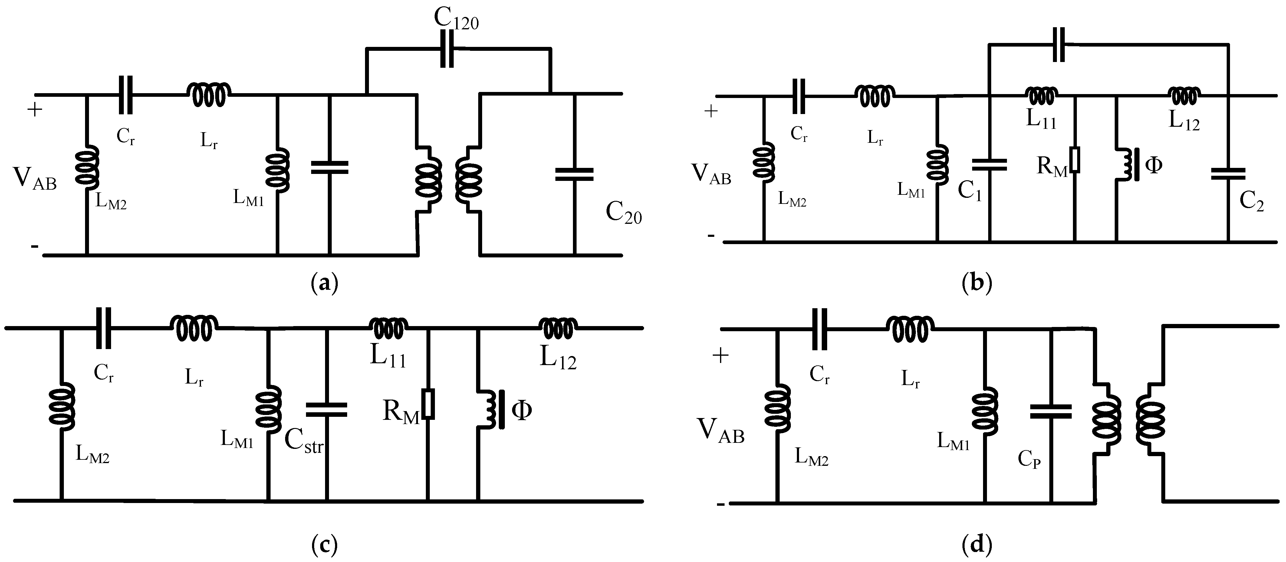
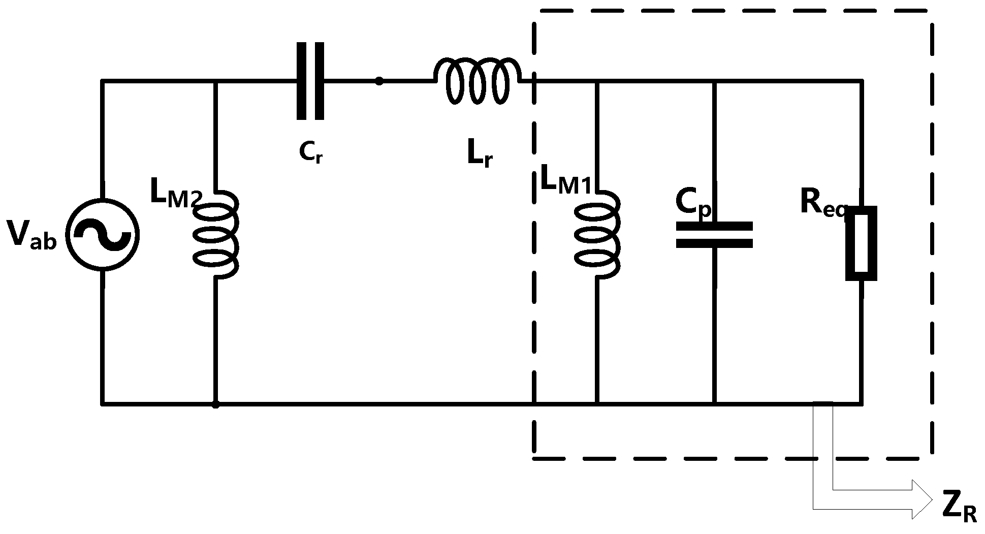
3.1. The LLC Model Considering Parasitic Capacitance

As Figure 4a shows, the transformer has two windings and stray capacitances. The resistance of the primary and secondary sides can be ignored due to less impact. C10 and C20 are the self-capacitance of the primary and secondary sides, respectively. C120 is the mutual capacitance of primary and secondary sides. The equivalent circuit of the transformer is shown in Figure 4b, in which the secondary parameters are represented by the primary. The specific relationship is shown in (3)–(5) [33].
C 1 = C 10 + ( 1 n ) C 120
C 2 = n 2 C 20 + n ( n 1 ) C 120
C 12 = n C 120
Since the leakage inductors are less than the magnetic inductor, the voltage drops across should be small. Therefore, C12 can be ignored, and the capacitance can be expressed by the Cstr. The final model is shown in Figure 4d. When the junction capacitance caused by the SR is considered, the parasitic capacitance equals the sum of the CSR and Cstr.
C s t r C 1 + C 2 C P C s t r + C S R
Before analyzing, some conditions need to be known. First, the switching frequency is greater than the resonant frequency under the light-load condition. Then, the switches are an ideal model that has no loss. Finally, the parasitic capacitance is juxtaposed with LM2.
At different times, the voltage and current have other states. Due to the newly added excitation inductor in the forward mode not playing one role in the resonant and the model being symmetrical, the forwarding mode should be analyzed. Meanwhile, the reversed mode is the same as the forward.
Mode1[t0-t1]: An equivalent circuit is shown in Figure 5a. S1 and S4 are on, and S2 and S3 are off. Before t0, the current flow of M1 and M4 is so that S1 and S4 are ZVS soft-switching. Due to the resonant inductor being smaller than excitation inductors and the parasitic capacitance Cp being smaller than the resonant capacitance, CP and Lr are in resonance. Meanwhile, the Vr is to zero, and iLm1 is similar to iLm2, as shown in Figure 6.
Mode2[t1-t2]: S1 and S4 are off, and S2 and S3 are on. The ir value is larger than iLm2, which flows the anti-diode of S2 and S4 for soft-switching in the following mode. ir covers the DC component, flowing LM1 at t1 time, and for the AC component, the resonant current generated by Cp and Lr. Uab is the reverse. Um also includes the DC, Vab, and AC parts as well as the resonance voltage generated by Cp and Lr. The voltage between Cr and Lr is approximately zero. The equivalent circuit is shown in Figure 5b.
Mode3[t2-t3]: The secondary side has limited the Cp voltage, which stops resonance with Lr. There is only one resonance where Cr and Lr occur in Figure 5c. This mode continues until the current that flows the resonance is equal to the excitation current iLM2. After this mode, the second half of the cycle begins when the current and voltage are symmetrical with the above modes.
The circuit is analyzed by the Fundamental Harmonic Approximation (FHA). When the load is minimal, the current and voltage are approximately in phase and can be regarded as a purely resistive load. The rectifier circuit can be equivalent to Req, as shown in (7).
R e q = 8 n 2 π 2 R L
where RL means the actual access load, and n means the ratio of the transformer. The input voltage V1 is approximately Vab, which is the value expressed by (8) adopting FHA. Vcd is the same thing.
V a b = 4 V 1 π sin ω t
V c d = 4 n V 2 π sin ω t
The relationship between the amplitude of Vab and the amplitude of Vcd can be obtained in Figure 7 by the principle of partial pressure.
G = V o u t V i n = | V c d V a b | = | Z L Z L + j ω L r + 1 j ω C r |
Z L = j ω L M 2 R e q j ω L M 2 + ( j ω ) 2 C p L M 2 R e q
After completion, the gain can be expressed as (12).
G = 1 ( 1 + 1 k λ x 2 1 k x + λ ) 2 + ( x 1 x ) 2 Q 2
λ = C p C r
where λ represents the Cp and Cr ratio; Figure 8 shows the gain curve according to (8). After the first wave, the switches achieve soft switching, reducing the loss; in other words, the whole circuit is in the inductive region. As the load decreases, the value of Q increases, and the voltage gain shows two spikes and a trough in Figure 8a. When Q is fixed, different λ values have different curves, as shown in Figure 8b. Drawing on the curves, as the parasitic capacitance increases, the second peak of the gain curve becomes larger. Therefore, the parasitic capacitance value is the most influential factor in the light-load stage, and the change of other parameters, such as the K value, is small. The gain curves need another Q, according to Figure 8b, in which Q is related to the λ.

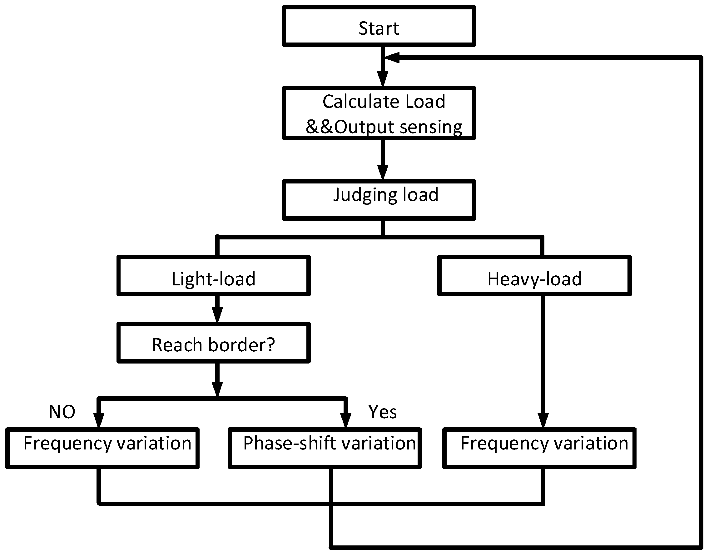
3.2. An Adopting Switching Control Method

The proposed control method applies to this model, solving the problem put forward in Section 2. In this section, one method is given: two degrees of freedom energy hysteresis control. This method which applies to the full load, particularly in light load, includes two parameters: frequency and phase-shift angle. In the reversed mode, the fundamental principles are similar to those of the forward mode. Therefore, only forward modes are analyzed here. The new control method based on this model improves output range, ensures output voltage stability, and enhances robustness, especially in light load.
The boundary between light load and heavy load is up to the circuit parameters. Light and heavy loads can be divided according to the gain curve. Taking the derivative of the gain, the following result can be obtained.
F ( x ) = 2 λ 2 x 8 [ 2 λ ( 1 + 1 k + λ ) Q 2 ] x 6 + [ 2 k ( 1 + 1 k + λ ) Q 2 ] x 2 2 k 2
In the paper, the curves with two sharp peaks are defined as a light load and the others are defined as a heavy load. Equation (14) has many positive solutions in the light load conditions, and the parameters are substituted into (14). After the actual load value is calculated from the output voltage and current obtained by sampling, the load value is substituted into (15) for comparison. When the load confirms to (15), the load can be defined as the light load.
R e q 2 > 1 2 L r C r C P 2 + C r ( 1 + L M 1 L r ) C P
The switching point varies in real time because of the value of the inductor and capacitance change with the frequency. The controller has entered the heavy-load mode when Req is too small to conform to (15). The circuit has adopted the conventional controller PFM control in the heavy load. The details about PFM are described in Section 2. In contrast, the gain has two peaks and one trough in the light-load situation. The circuit adopts the two-degree-of-freedom energy hysteresis control. This control method includes two modulation strategies, phase shift and frequency. Before the frequency reaches the switch, the circuit enters PFM mode in light load, as in heavy load. The frequency gradually decreases with the load increase.
In the PSM mode, the switching frequency is beyond resonance frequency in the light load conditions, and Figure 9 is only a schematic diagram of the waveform in PFM mode without specific values. The amplitude of the curve is determined by the input, load, device parameters, control method, etc. S1, S2, S3 and S4 are complementary in one period. As Figure 9 shows, when Vab is beyond zero, ir grows up. When Vab approaches zero in one period, Cp and Lr are resonant. In the second half of the period, the process is similar. There exists a phase shift between S1 and S4, which can effectively reduce the voltage at a higher voltage side. As the phase shift angle increases gradually, the voltage in the positive mode also decreases progressively until the phase shift angle reaches the maximum and the voltage reaches the minimum. The angle limit range is [ 0 , 0.5 ] . It is shown that the relationship between voltage and phase-shift in Figure 10 is identical to the linear. The frequency after arriving at the switching point is fixed, which is the same as the switching point. The PS mode adopts the PI controller to change the phase angle, which magnifies gradually with the load. The switch point is the critical matter which relates to mode switching. The boundary selection should consider the performance of the two modes and characteristics.
When switching, the output voltage must be highly smooth and reduce the voltage spike. The rate of voltage change needs to be small. Therefore, the output voltage and frequency rate of change are set as reference values. When the rate equals zero, the output curve at the switch point is the most smooth. As Figure 11 shows, tanθ is up to the ratio of ΔVO and Δfs, which is so tiny. The red line represents the relationship between output and frequency, and the blue line represents the approximation relationship between the two. The value of tanθ approximates the derivative as (16).
tan θ = U o u t f s d U o u t d f s
U O U T = U 2 U 1
f = f 1 f 2
Since the input voltage is constant, the output voltage and frequency relationship approximately equal the gain curve and frequency. The output is replaced with the gain for calculating. Consequently, the point is chosen when tanθ is approximately minimum, where the output is kept smooth. As the input is kept constant, (16) is approximately the derivative of (12).
According to (14), there are four solutions, three of which are greater than zero in the light load situation. There are three possible values for XB. Since the switching point is related to the circuit parameters, in practice, XB is less than or equal to 1 when the circuit parameters are extreme. So, it makes no sense to discuss XB in the above situations. The switching point gradually moves to the left when the Q increases until it switches to the heavy load mode. When the frequency reaches XB, the phase shift has maintained the initial value in the first period, and the phase shift is variable in the next period.
Due to there being more interference from new energy sources, when it is near the switching point, the modes are switched several times, resulting in system instability. In order to avoid the above situation, hysteresis control is introduced. Hysteresis control can reduce the number of switching and maintain the robustness of control under frequent disturbance. When the system is perturbed in the hysteresis range, the system retains its previous mode. Energy hysteresis control is a range for shock within a limit. Its control includes two directions, heavy-load to light-load and light-load to heavy-load, as shown in Figure 12. After frequency reaching the switching point for the first time in the first direction, the energy hysteresis is trigged, and the converter enters the phase shift mode. The calculated frequency experiences shocks between XB1 and XB2 but does not switch mode. In other words, the frequency is fixed at this shocking stage. When the calculated frequency is left of the XB1, the mode has been changed, switching to PFM mode. The phase shift gradually decreases from light to heavy load. After the calculated frequency reaches the switching point, the mode has been switched to PFM mode, and energy hysteresis control plays a role. The phase angle is changed only when the calculated frequency reaches XB2.
The actual tolerance range for the output voltage has influenced the hysteresis range. The hysteresis range depends on the demand for voltage variation under different load conditions. The output voltage is proportional to load and inversely proportional to parasite capacitance and sampling accuracy. When the load is light, the voltage varies greatly with frequency. According to the gain curve, XB1 and XB2 are large at this time. When the load is slightly heavy, the hysteresis range is small. When the circuit requires high precision of the output voltage, the hysteresis range is small, and the voltage transition is relatively unstable. When the accuracy is low, the hysteresis range is large. Overall, the length increases with the value of Q in Figure 12. As shown in Figure 13, the LLC control method has many steps that ensure robustness and output constant.

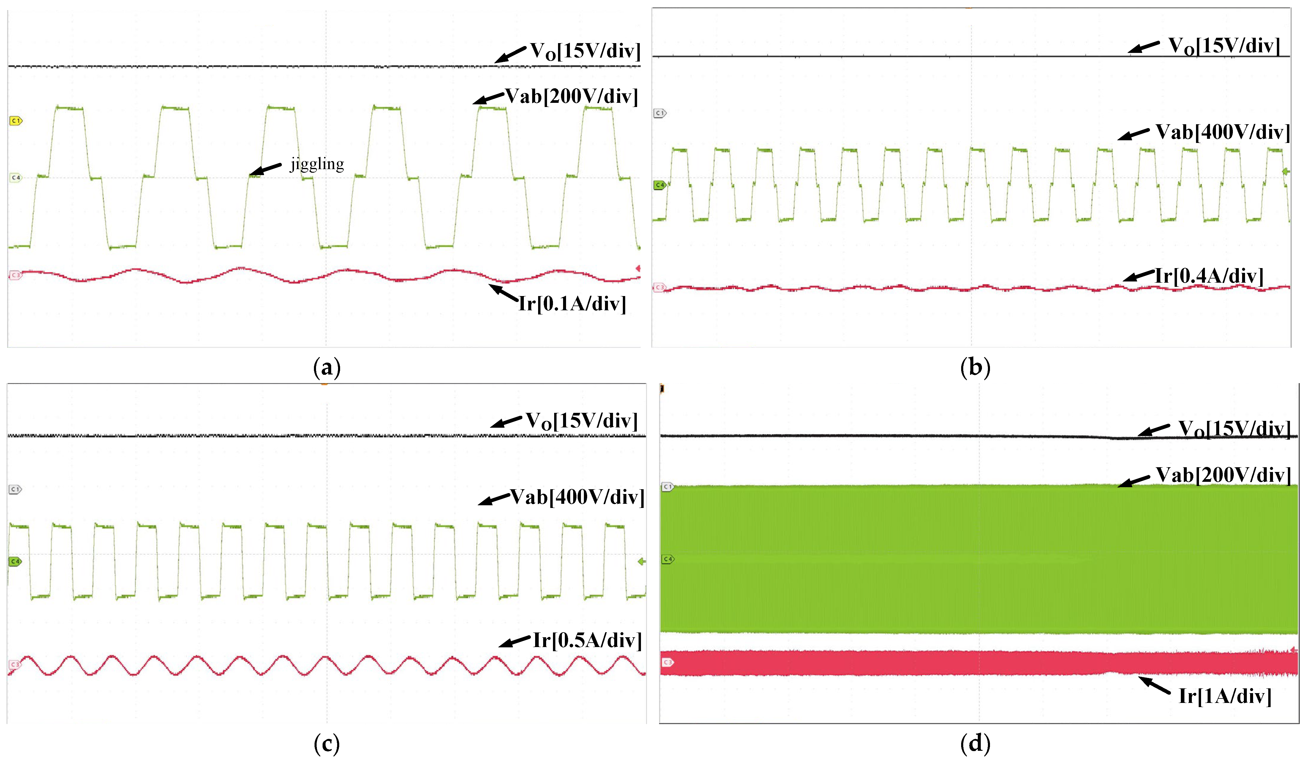
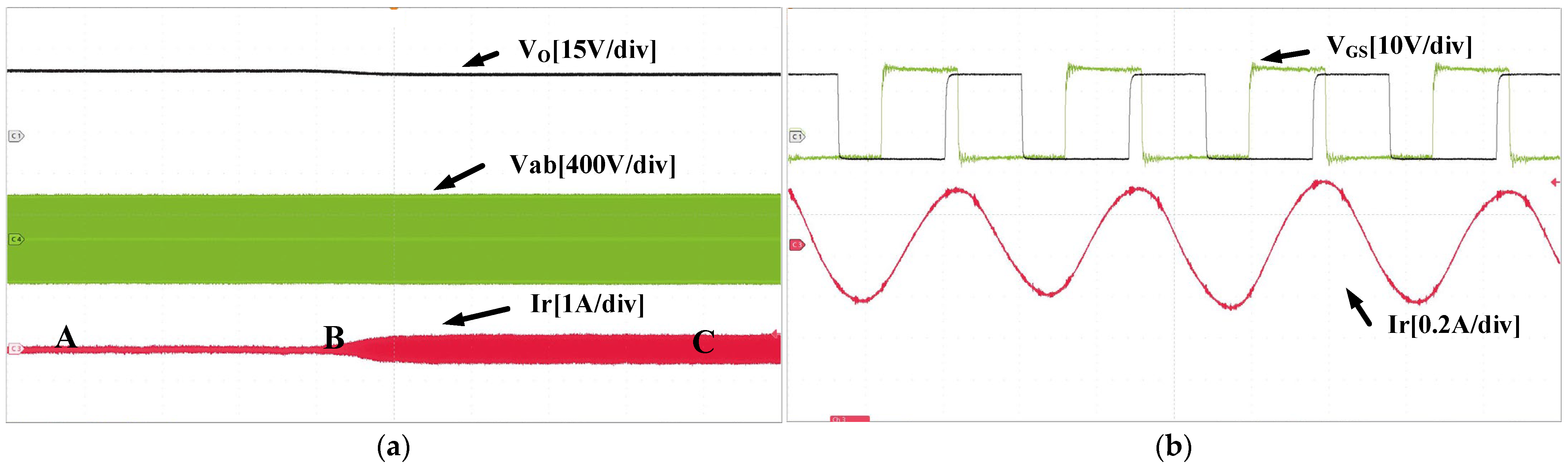
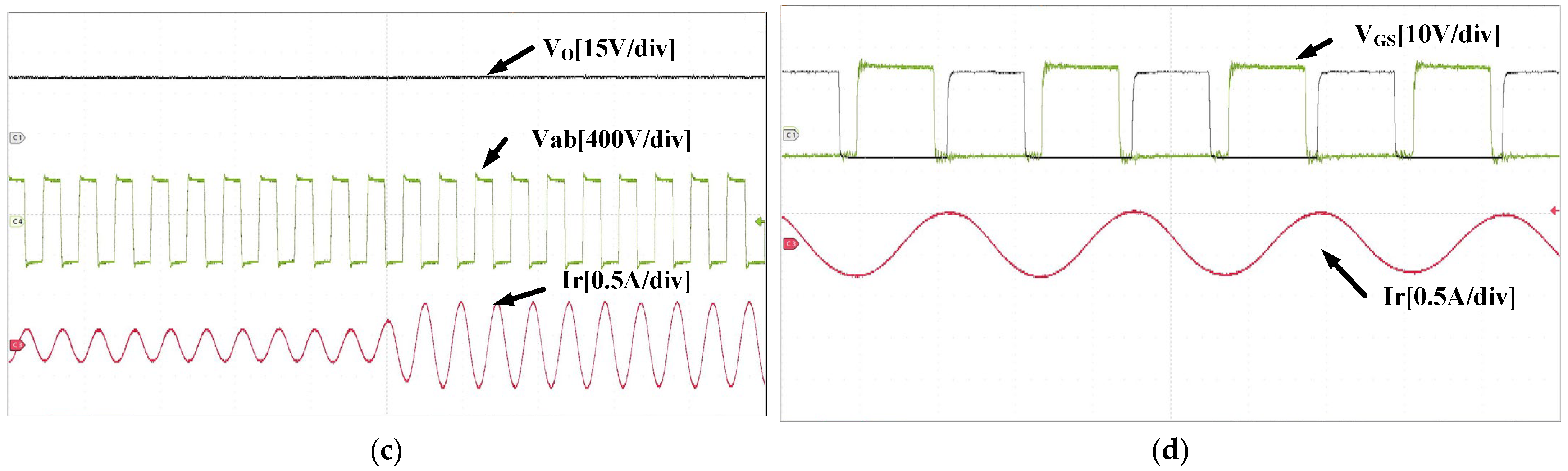
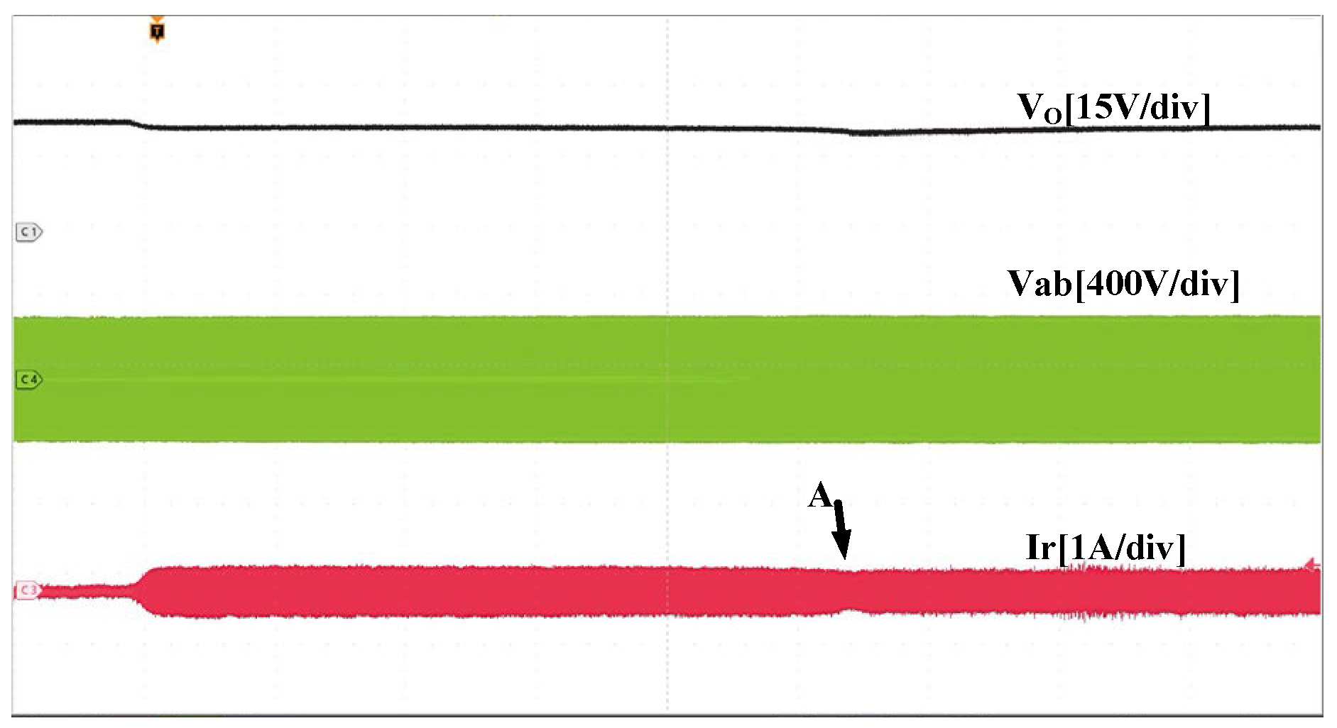
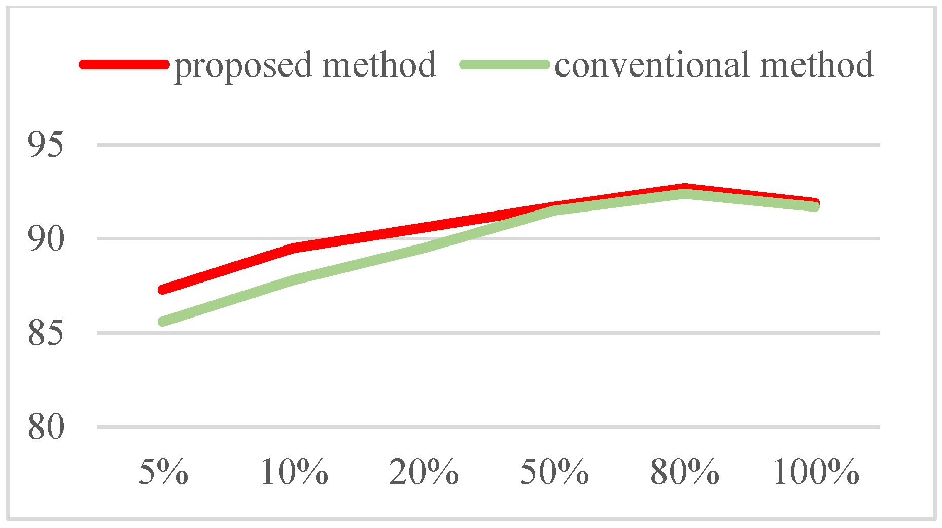
4. Experimental Results

The prototype is designed to connect the input to the inverter and the output to the energy storage device. The prototype works in Vin = 400 V in the forward mode, while the reference is kept constant at 36 V. The maximum output current is 27 A in forwarding mode and 2.5 A in reverse mode. The theoretical value of the resonant frequency is the same as the switching frequency, but some parasitic parameters cause the resonant frequency to be slightly below 100 K. NTHL160N120SC1 and IXFH160N15T2 are chosen as the primary and secondary MOSFETs, respectively. Detailed parameters are shown in the table. Those devices are larger than the values calculated to leave a margin. So, the capacitance is chosen to be 24.6 uh, and the transformer is made to have a turn ratio of 12. LM1 and LM2 hold to make the prototype symmetry, and the detailed parameters in the prototype is shown in Table 1. The prototype is shown in Figure 14. It should be mentioned that this prototype is only for verification of principle and does not pursue power density.
DSP, TMS320F28335, which is published by Texas Instruments, is used as the digital processing unit, which +5 V supplies. The DSP is connected to the upper computer as a key to the grid. The DSP consists of the PWM generator, an analogue-to-digital converter (ADC), a sampling module, and a delay-time module. The output voltage and current collected by the Hall element are transformed into digital quantities by the ADC module for control. According to the proposed method, the frequency and phase shift are adjusted by the PI controller. We use the look-up table in DSP to obtain the switching point, which is limited by data processing capability, and the lengths are calculated in real time.
Waveforms are shown in Figure 15, including the output voltage, midpoint voltage of the H-bridge, and the current flowing through the resonance cavity at a steady state. They are laid out in proper order at 1% load, 5% load,10% load, and 30% load. VAB has some jigglings due to the parasite capacitance. The switches can achieve the soft-switching of ZVS and ZCS in this condition where Vin = 400 V, VO = 36 V in the forward mode. The control mode in Figure 5a,b is the PSM mode, and there is the phase shift between M1 and M4, in which the phase shift at 1% load is greater. The frequency increases as the load becomes heavier when in PFM mode.
In Figure 16, the load varies from 8% to 25%. The resonance current increases from 0.1 to 0.8 A, while the output voltage decreases by 0.2 V. At the moment when the load varies, there is no burr on the output voltage and resonance current. Figure 16a shows the whole process of variable load, and Figure 16b–d correspond to A, B, and C in Figure 16a, respectively. The load at point B increases. Due to the dead-time being set too long and DSP needing some computation time, the variation on the Vab when the load varies is not outstanding. The driving waveforms of point A and point C are shown. At point A, the driving waveform of M1 overlaps that of M4, and the overlap is the phase shift angle. The frequency is adjusted by the digital controller at point C, where the frequency is minor until the output equals the reference.
Figure 17 shows the energy hysteresis control. Point A means jumping out of energy hysteresis control after changing the load. The proposed method decreases the burr when varying the load and has strong robustness. From Figure 18, it is easy to see that the efficiency of the proposed control method is higher than that of conventional PFM, especially in light load conditions. The THDv for this control method is 0.45% in the steady state, whose output voltage is calculated by Fourier.

5. Conclusions

An adaptive switching control method is proposed to keep the output voltage constant based on the LLC model considering parasitic capacitance. In this control method, the frequency is adjusted according to the gain curve to ensure the continuity of control, and in light load conditions, the phase shift is regulated to maintain constant. Meanwhile, the switching point is calculated according to the characteristics to switch smoothly. An adaptive control method around the switching point has been proposed, strengthening the robustness disturbance, especially in light load conditions. Compared with other control methods, the proposed control method can solve the voltage problem of reverse bias and light load simultaneously. It is simple enough to be practical. In the face of slight disturbance near the switching point, it can also maintain stability and keep the system stable. Experimental data using the 400V–36V–1kW prototype converter verify the validity of the proposed model and control method for ensuring constant output voltage, especially under frequent disturbances.

Author Contributions

Project administration, R.W., Y.Z. and D.M.; Software, S.J. and L.W.; Writing—original draft, Y.H. All authors have read and agreed to the published version of the manuscript.

Funding

This research was funded by the Fundamental Research Funds for the Central Universities grant number N2204007 and by the State Key Laboratory of Alternate Electrical Power System with Renewable Energy Sources grant number No.LAPS22002.

Institutional Review Board Statement

Not applicable.

Informed Consent Statement

Not applicable.

Conflicts of Interest

The authors declare no conflict of interest.

References

  1. Gao, S.; Zhao, H.; Gui, Y.; Luo, J.; Blaabjerg, F. Impedance Analysis of Voltage Source Converter Using Direct Power Control. IEEE Trans. Energy Convers. 2020, 36, 831–840. [Google Scholar] [CrossRef]
  2. Gao, S.; Zhao, H.; Wang, P.; Gui, Y.; Terzija, V.; Blaabjerg, F. Comparative Study of Symmetrical Controlled Grid-Connected Inverters. IEEE Trans. Power Electron. 2021, 37, 3954–3968. [Google Scholar] [CrossRef]
  3. Xie, F.; McEntee, C.; Zhang, M.; Mather, B.; Lu, N. Development of an Encoding Method on a Co-Simulation Platform for Mitigating the Impact of Unreliable Communication. IEEE Trans. Smart Grid 2020, 12, 2496–2507. [Google Scholar] [CrossRef]
  4. Alawieh, H.; Riachy, L.; Arab Tehrani, K.; Azzouz, Y.; Dakyo, B. A new dead-time effect elimination method for H-bridge inverters. In Proceedings of the IECON 2016—42nd Annual Conference of the IEEE Industrial Electronics Society, Florence, Italy, 23–26 October 2016; pp. 3153–3159. [Google Scholar]
  5. Zhao, H.; Wu, Q.; Wang, J.; Liu, Z.; Shahidehpour, M.; Xue, Y. Combined Active and Reactive Power Control of Wind Farms Based on Model Predictive Control. IEEE Trans. Energy Convers. 2017, 32, 1177–1187. [Google Scholar] [CrossRef]
  6. Montero-Cassinello, J.; Cheah-Mane, M.; Prieto-Araujo, E.; Gomis-Bellmunt, O. Small-signal analysis of a fast central control for large scale PV power plants. Int. J. Electr. Power Energy Syst. 2022, 141, 108157. [Google Scholar] [CrossRef]
  7. Gao, S.; Zhao, H.; Gui, Y.; Zhou, D.; Terzija, V.; Blaabjerg, F. A Novel Direct Power Control for DFIG with Parallel Compensator Under Unbalanced Grid Condition. IEEE Trans. Ind. Electron. 2020, 68, 9607–9618. [Google Scholar] [CrossRef]
  8. Faraji, R.; Adib, E.; Farzanehfard, H. Soft-switched non-isolated high step-up multi-port DC-DC converter for hybrid energy system with minimum number of switches. Int. J. Electr. Power Energy Syst. 2018, 106, 511–519. [Google Scholar] [CrossRef]
  9. Li, H.; Zhao, L.; Xu, C.; Zheng, X. A Dual Half-Bridge Phase-Shifted Converter with Wide ZVZCS Switching Range. IEEE Trans. Power Electron. 2017, 33, 2976–2985. [Google Scholar] [CrossRef]
  10. Chen, Z.; Liu, S.; Shi, L. A Soft Switching Full Bridge Converter with Reduced Parasitic Oscillation in a Wide Load Range. IEEE Trans. Power Electron. 2014, 29, 801–811. [Google Scholar] [CrossRef]
  11. Chan, Y.P.; Loo, K.H.; Yaqoob, M.; Lai, Y.M. A Structurally Reconfigurable Resonant Dual-Active-Bridge Converter and Modulation Method to Achieve Full-Range Soft-Switching and Enhanced Light-Load Efficiency. IEEE Trans. Power Electron. 2018, 34, 4195–4207. [Google Scholar] [CrossRef]
  12. Shi, H.; Wen, H.; Chen, J.; Hu, Y.; Jiang, L.; Chen, G.; Ma, J. Minimum-Backflow-Power Scheme of DAB-Based Solid-State Transformer with Extended-Phase-Shift Control. IEEE Trans. Ind. Appl. 2018, 54, 3483–3496. [Google Scholar] [CrossRef]
  13. Wang, K.; Wei, G.; Wei, J.; Wu, J.; Wang, L.; Yang, X. Current Detection and Control of Synchronous Rectifier in High-Frequency LLC Resonant Converter. IEEE Trans. Power Electron. 2022, 37, 3691–3696. [Google Scholar] [CrossRef]
  14. Wu, X.; Hua, G.; Zhang, J.; Qian, Z. A New Current-Driven Synchronous Rectifier for Series–Parallel Resonant (LLC) DC–DC Converter. IEEE Trans. Ind. Electron. 2010, 58, 289–297. [Google Scholar] [CrossRef]
  15. Feng, W.; Mattavelli, P.; Lee, F.C. Pulsewidth Locked Loop (PWLL) for Automatic Resonant Frequency Tracking in LLC DC–DC Transformer (LLC-DCX). IEEE Trans. Power Electron. 2012, 28, 1862–1869. [Google Scholar] [CrossRef]
  16. Li, H.; Wang, S.; Zhang, Z.; Zhang, J.; Zhu, W.; Ren, X.; Hu, C. A Bidirectional Synchronous/Asynchronous Rectifier Control for Wide Battery Voltage Range in SiC Bidirectional LLC Chargers. IEEE Trans. Power Electron. 2021, 37, 6090–6101. [Google Scholar] [CrossRef]
  17. Li, H.; Zhang, Z.; Wang, S.; Tang, J.; Ren, X.; Chen, Q. A 300-kHz 6.6-kW SiC Bidirectional LLC Onboard Charger. IEEE Trans. Ind. Electron. 2020, 67, 1435–1445. [Google Scholar] [CrossRef]
  18. Fei, C.; Li, Q.; Lee, F.C. Digital Implementation of Adaptive Synchronous Rectifier (SR) Driving Scheme for High-Frequency LLC Converters with Microcontroller. IEEE Trans. Power Electron. 2017, 33, 5351–5361. [Google Scholar] [CrossRef]
  19. Xue, B.; Wang, H.; Liang, J.; Cao, Q.; Li, Z. Phase-Shift Modulated Interleaved LLC Converter with Ultrawide Output Voltage Range. IEEE Trans. Power Electron. 2020, 36, 493–503. [Google Scholar] [CrossRef]
  20. Jovanovic, M.M.; Irving, B.T. On-the-Fly Topology-Morphing Control—Efficiency Optimization Method for LLC Resonant Converters Operating in Wide Input- and/or Output-Voltage Range. IEEE Trans. Power Electron. 2016, 31, 2596–2608. [Google Scholar] [CrossRef]
  21. Buccella, C.; Cecati, C.; Latafat, H.; Pepe, P.; Razi, K. Observer-Based Control of LLC DC/DC Resonant Converter Using Extended Describing Functions. IEEE Trans. Power Electron. 2015, 30, 5881–5891. [Google Scholar] [CrossRef]
  22. Li, H.; Wang, S.; Zhang, Z.; Zhang, J.; Li, M.; Gu, Z.; Ren, X.; Chen, Q. Bidirectional Synchronous Rectification on-Line Calculation Control for High Voltage Applications in SiC Bidirectional LLC Portable Chargers. IEEE Trans. Power Electron. 2020, 36, 5557–5568. [Google Scholar] [CrossRef]
  23. Kirshenboim, O.; Peretz, M.M. Combined Multilevel and Two-Phase Interleaved LLC Converter with Enhanced Power Processing Characteristics and Natural Current Sharing. IEEE Trans. Power Electron. 2017, 33, 5613–5620. [Google Scholar] [CrossRef]
  24. Jung, J.H.; Kim, H.S.; Ryu, M.H.; Baek, J.W. Design Methodology of Bidirectional CLLC Resonant Converter for High-Frequency Isolation of DC Distribution Systems. IEEE Trans. Power Electron. 2013, 28, 1741–1755. [Google Scholar] [CrossRef]
  25. Jiang, T.; Zhang, J.; Wu, X.; Sheng, K.; Wang, Y. A Bidirectional LLC Resonant Converter with Automatic Forward and Backward Mode Transition. IEEE Trans. Power Electron. 2014, 30, 757–770. [Google Scholar] [CrossRef]
  26. Jiang, T.; Zhang, J.; Wu, X.; Sheng, K.; Wang, Y. A Bidirectional Three-Level LLC Resonant Converter with PWAM Control. IEEE Trans. Power Electron. 2016, 31, 2213–2225. [Google Scholar] [CrossRef]
  27. Awasthi, A.; Bagawade, S.; Jain, P.K. Analysis of a Hybrid Variable-Frequency-Duty-Cycle-Modulated Low-Q LLC Resonant Converter for Improving the Light-Load Efficiency for a Wide Input Voltage Range. IEEE Trans. Power Electron. 2020, 36, 8476–8493. [Google Scholar] [CrossRef]
  28. Hu, Z.; Qiu, Y.; Wang, L.; Liu, Y.-F. An Interleaved LLC Resonant Converter Operating at Constant Switching Frequency. IEEE Trans. Power Electron. 2013, 29, 2931–2943. [Google Scholar] [CrossRef]
  29. Yoon, H.; Lee, H.; Ham, S.; Choe, H.; Kang, B. Off-Time Control of LLC Resonant Half-Bridge Converter to Prevent Audible Noise Generation Under a Light-Load Condition. IEEE Trans. Power Electron. 2018, 33, 8808–8817. [Google Scholar] [CrossRef]
  30. Fei, C.; Gadelrab, R.; Li, Q.; Lee, F.C. High-Frequency Three-Phase Interleaved LLC Resonant Converter with GaN Devices and Integrated Planar Magnetics. IEEE J. Emerg. Sel. Top. Power Electron. 2019, 7, 653–663. [Google Scholar] [CrossRef]
  31. Tehrani, K.; Capitaine, T.; Barrandon, L.; Hamzaoui, M.; Rafiei, S.M.R.; Lebrun, A. Current control design with a fractional-order PID for a three-level inverter. In Proceedings of the 2011 14th European Conference on Power Electronics and Applications, Birmingham, UK, 30 August 2011–1 September 2011; pp. 1–7. [Google Scholar]
  32. Priya, M.; Ponnambalam, P. Circulating Current Control of Phase-Shifted Carrier-Based Modular Multilevel Converter Fed by Fuel Cell Employing Fuzzy Logic Control Technique. Energies 2022, 15, 6008. [Google Scholar] [CrossRef]
  33. Lu, H.Y.; Zhu, J.G.; Hui, S. Experimental determination of stray capacitances in high frequency transformers. IEEE Trans. Power Electron. 2003, 18, 1105–1112. [Google Scholar] [CrossRef] [Green Version]
Figure 1. The conventional L-LLC.
Sustainability 14 11832 g001
Figure 2. The gain curve of the conventional model.
Sustainability 14 11832 g002
Figure 3. Control blocks of the proposed universal adaptive SR driving scheme.
Sustainability 14 11832 g003
Figure 4. Models including parasitic capacitances (a) circuit model (b,c) equivalent circuit model (d) simplified model.
Sustainability 14 11832 g004
Figure 5. The model with parasitic capacitance (a) t0-t1 (b) t1-t2 (c) t2-t3.
Sustainability 14 11832 g005
Figure 6. Waveforms of the circuit in PFM.
Sustainability 14 11832 g006
Figure 7. The simplified model with the parasitic capacitance.
Sustainability 14 11832 g007
Figure 8. The gain curve of the new model: (a) the gain curve under different Q, (b) the gain curve under different λ.
Sustainability 14 11832 g008
Figure 9. Waveforms of the circuit in PSM.
Sustainability 14 11832 g009
Figure 10. The relationship between phase shift and VAB.
Sustainability 14 11832 g010
Figure 11. The diagram for the switching point.
Sustainability 14 11832 g011
Figure 12. The diagram of the energy hysteresis.
Sustainability 14 11832 g012
Figure 13. Diagram for the proposed control.
Sustainability 14 11832 g013
Figure 14. The prototype for the LLC.
Sustainability 14 11832 g014
Figure 15. Under different loads: (a) 1% load, (b) 5% load, (c) 10% load, (d) 30% load.
Sustainability 14 11832 g015
Figure 16. The load from 8% to 25%: (a) overview, (b) light load, (c) switching point, (d) heavy load.
Sustainability 14 11832 g016aSustainability 14 11832 g016b
Figure 17. The energy hysteresis control.
Sustainability 14 11832 g017
Figure 18. Efficiency curves of the prototype.
Sustainability 14 11832 g018
Table 1. Detailed parameters in the prototype.
ParametersValue
Resonance inductorLr = 101 μH
Resonance capacitanceCr = 24.6 μH
Magnetic inductanceLM1 = LM2 = 606 μH
Ratio of transformern = 12
Publisher’s Note: MDPI stays neutral with regard to jurisdictional claims in published maps and institutional affiliations.

