Review

A Comprehensive Review on Graphene Nanoparticles: Preparation, Properties, and Applications

by
Talal Yusaf
1,2,*,
Abu Shadate Faisal Mahamude
3,
Kaniz Farhana
4,
Wan Sharuzi Wan Harun
3,
Kumaran Kadirgama
5,6,
Devarajan Ramasamy
3,
Mohd Kamal Kamarulzaman
5,
Sivarao Subramonian
7,
Steve Hall
1 and
Hayder Abed Dhahad
8
1
School of Engineering and Technology, Central Queensland University, Rockhampton, QLD 4701, Australia
2
Department of Research, Universiti Tenaga Nasional, Kajang 43000, Selangor, Malaysia
3
Department of Mechanical Engineering, College of Engineering, Universiti Malaysia Pahang, Gambang 26300, Pahang, Malaysia
4
Department of Apparel Engineering, Bangladesh University of Textiles, Dhaka 1208, Bangladesh
5
Automotive Engineering Centre, Universiti Malaysia Pahang, Pekan 26600, Pahang, Malaysia
6
Faculty of Mechanical and Automotive Engineering Technology, Universiti Malaysia Pahang, Pekan 26600, Pahang, Malaysia
7
Faculty of Manufacturing Engineering, Universiti Teknikal Malaysia Melaka, 76100 Melaka, Melaka, Malaysia
8
Mechanical Engineering Department, University of Technology-Iraq, Baghdad 10066, Iraq
*
Author to whom correspondence should be addressed.
Sustainability 2022, 14(19), 12336; https://doi.org/10.3390/su141912336
Submission received: 21 August 2022 / Revised: 14 September 2022 / Accepted: 16 September 2022 / Published: 28 September 2022
(This article belongs to the Section Waste and Recycling)

Abstract

:
Graphene, with its amazing prospects and nonpareil aspects, has enticed scientists and researchers all over the globe in a significant fashion. Graphene, the super material, endlessly demonstrates some of the substantial, as well as desired, mechanical, thermal, optical, and chemical characteristics which are just about to bring about an unprecedented transformation in the science and technology field. Being derived from graphite, graphene is made of one-atom-thick, two-dimensional carbon atoms arranged in a honeycomb lattice. This Nobel-prize-winning phenomenon includes properties that may result in a new dawn of technology. Graphene, the European Union’s (EU) largest pledged project, has been extensively researched since its discovery. Several stable procedures have been developed to produce graphene nanoparticles in laboratories worldwide. Consequently, miscellaneous applications and futuristic approaches in artificial intelligence (AI)-based technology, biomedical and nanomedicine, defence and tactics, desalination, and sports are ruling over the next generation’s fast-paced world and are making the existing market competitive and transformative. This review sheds light upon the ideology of the preparation and versatile application of graphene and foretells the upcoming advancements of graphene nanoparticles with the challenges rearing ahead. The study also considers graphene nanoparticles’ diverse fields and portends their sustainability with the possibility of their acceptance in the commercial market as well as in common usage.

1. Introduction

Carbon atoms are arranged to form graphene in a hexagonal structure. It is a triangular grid with two atomic bases rather than a Bravais grid [1]. As can be seen from the number of articles published each year and the considerable amount of investment in research, international interest in this “wonder material” is still growing [2]. This interest stems primarily from the multifunctionality of the 2D atomic crystal, which combines outstanding features, such as thermal conductivity of around 5000 W/m·K [3]. Even as charge carrier concentrations approach zero, graphene’s conductivity never falls below a minimum value equivalent to the quantum unit of conductance. At room temperature, graphene possesses excellent electron fluidity (250,000 cm2/V·s) [4], a large surface area (2630 m2/g) [5], and a high modulus of elasticity (~1 TPa). It has strong electrical conductivity, making it suitable for use in a wide range of applications. High-end composite materials are amongst the potential applications [6,7], as are field-effect transistors [8], electromechanical systems [9], strain sensors [10], supercapacitors [11], hydrogen storage systems [12,13], and solar cells [14,15,16]. Due to its 2D planar structure and the fact that it is a zero-gap semimetal, the utilization of graphene in some applications is more challenging. Graphene, therefore, has been treated in several forms, such as nanoribbons [17], quantum points for usage in hydrogels and semiconductor devices [18,19], and nitrogen-doped graphene foams [20,21] for biological and energy applications [22].
The effect of the size, shape and some nanoparticles of different graphene-based nanomaterials (i.e., GO, RGO GQD, GNPs, GONs) requires further investigation. The majority of the literature and findings about graphene presented by researchers are based on the physical and thermal features and innovative notions and theorems. However, a good amount of literature featuring the economic feasibility of graphene nanoparticles, industrial justifications of costing, and production efficiency reports still needs to be researched, as well as published, to carry on the process. The challenge of maintaining enough graphene dispersion is a unique characteristic that needs to be overcome to take advantage of the unique properties of graphene (at least in bulk systems). In both academic circles and industry, the study of the mechanical features of graphene composites is becoming increasingly popular. This review presents updates on publications found during our research on the mechanics of graphene composites [23].
Recent advances in atomically thin, two-dimensional (2D) materials have led to various promising future technologies for post-CMOS nanoelectronics and energy generation [24,25,26]. For example, graphene, a one-atom-thick planar sheet of carbon atoms densely packed in a honeycomb crystal lattice, has grabbed appreciable attention due to its exceptional electronic and optoelectronic properties. The reported properties and applications of this two-dimensional carbon structure form have opened up new opportunities for future devices and systems. However, although graphene is known as one of the best electronic materials, synthesizing a single sheet of graphene has been less explored [27]. Nevertheless, graphene-based nanomaterials are promising in many utilizations due to their momentous basic, engineered, and genuine properties [28,29,30].
Graphene is the most straightforward, most robust material that has ever been found and has shown its capacity in various fields. In addition, graphene has consolidated itself as an invaluable material whereby many applications can be improved or revised in the existing paradigm. It has provoked a good response in the commercial field of synthesis and processing, construction, electronics, energy storage, telecommunications, composites, military and defence, aerospace, biomedicine, energy generation, and automotive industries. As seen in the given pie diagram (Figure 1), we observed that the most significant portion of graphene is used in the electronics and energy storage sector as well as in the aerospace sector, which means graphene is a driver of modern technology applications [31].
The ability of graphene to absorb near-infrared light has been demonstrated using magnetic resonance excitation in metamaterials. At the communication wavelength of 1550 nm, the absorption maximum of monolayer graphene can reach up to 77%. The absorption bandwidth is commonly defined. When the incident angle is increased even to 60 degrees for both p and s polarizations, the absorption maximum, absorption bandwidth, and resonance position all show almost no change. The absorption in graphene can be completely modulated with a nearly 100% modulation depth by applying an external bias voltage to change the Fermi energy. Furthermore, the absorption of graphene changes abruptly and dramatically around the interbond transition, exhibiting an electrical switching property [32]. Placing the graphene layer on the top layer of the PT symmetry photonic crystal to design a composite structure of graphene and parity–time (PT) symmetry photonic crystal can realize the ultra-strong absorption of graphene with electrical modulation properties. The absorption properties of graphene and, therefore, the electrical modulating properties of the structure were theoretically analyzed using the transfer matrix method in a paper. The modulation depth of graphene absorption approached 100%, and the operation speed was near 8.171 GHz [33]. Because of its excellent conductivity, high transmittance, and flexibility, graphene, which is made up of single-layer carbon atoms arranged in the shape of a unique, hexagonal honeycomb lattice structure, is a promising, two-dimensional, transparent, conductive material for flexible organic light-emitting devices (FOLED) [34]. Light absorption enhancement in graphene is desired for many applications in optoelectronic devices (e.g., photodetectors) [35]. It is well known that the optical wavelength range absorption efficiency of suspended monolayer graphene is only 2.3%. Dual-band absorption enhancement of monolayer graphene at optical frequency has been numerically demonstrated, with the most absorption efficiency reaching around 70% under ideal conditions. As per its inherent optical properties and lightweight absorption frequency, graphene produces exceptional thermal conductivity to other nanomaterials [36].
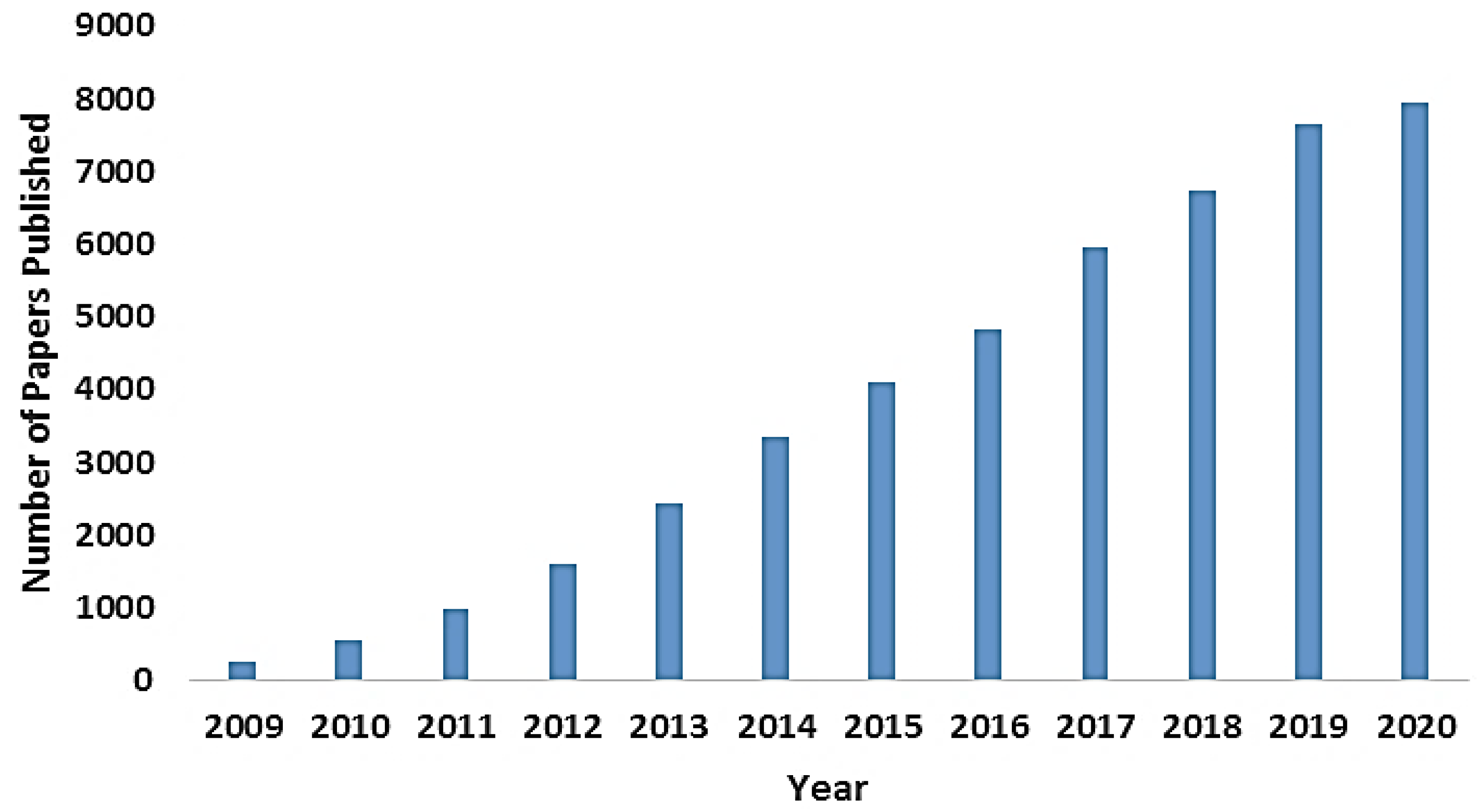
Since graphene is just a single layer of carbon atoms connected in a hexagonal pattern, it is also extremely thin and lightweight and an attractive material for nanotechnology applications. On the other hand, the increasing number of graphene publications in journals, as shown in Figure 2, shows the importance of graphene after innovation. This work consists of a consolidated review of graphene’s exotic properties, different manufacturing approaches, characteristics, and promising graphene applications. This review is followed by a debate summarizing these activities and possible applications in the future and some recommendations.

2. Graphene Basic Structure

2.1. Basic Mechanical Structure of Graphene

Carbon is placed as the sixth element in the periodic table with an electronic 1s22s22Px12Py12Pz0 ground state configuration, as illustrated in Figure 3b. The 2pz energy level is stabilized without electrons for convenience but equals the 2px and 2py energies. As shown in Figure 3a, of the six electrons, the four remaining in the outer shell are valence electrons, which encircle the nucleus of a carbon atom. These electrons can form three hybridization types in a carbon valence shell, namely, sp, sp2, and sp3. The formation of hybrids of sp2 is shown in Figure 3c. Since carbon atoms share sp2 electrons with their three nearby carbon atoms, they form a planar structure wave network layer, which is also called a monolayer graph. The graphene crystal unit cell is shown in Figure 3d, marked by a purple parallelogram, which has the same gate constant of 2.45 Å, and two carbon atoms. The stability of the planar ring is caused by the resonance and the relocation of electrons. The out-of-plane Ś bond is made by 2pz orbitals perpendicular to the planar structure, with a typical sp2 hysteria [37] of the two neighbouring carbon atoms on the graphene layer (see Figure 3e), while the in-plane bond is formed by the sp2 hybrid orbits (2s, 2px, and 2py). The resulting covalent μ bond is a short-length interatomic ~1.42 Å, making it more robust than the hybridized carbon/carbon diamond sp3 bonds. The monolayers of graphs, therefore, have remarkable mechanical properties (for example, a 1 TPa Young’s modulus and 130.5 GPa intrinsic strength) [38,39,40].
As the half-filled μ band allows free moving of electrons, the steering band and valence band with zero band distances are created in a monolayer graph [39]. In addition, the α bonds give a weak interaction of Van der Waals forces adjacent to the graphene layers of two-layer and multilayer graphene.

2.2. Electrical Band Structure of Graphene

Graphene can be tailored chemically and structurally in many ways without losing its structure and electronic flexibility or its metal atomic deposition. In new directions, graphene-based systems with magnetic and superconducting features may be regenerated to control graphene properties. Understanding and controlling this material’s properties are open doors in electronics for a new frontier with modern dimensions [40]. The band structure is studied most often from the point of view of the relationship between electron energy and momentum in each material. Since the graph limits the movement of the electrons to two dimensions, we also limit our momentum space to two dimensions. Therefore, an energy-to-energetic relationship can be found for graphene [41].
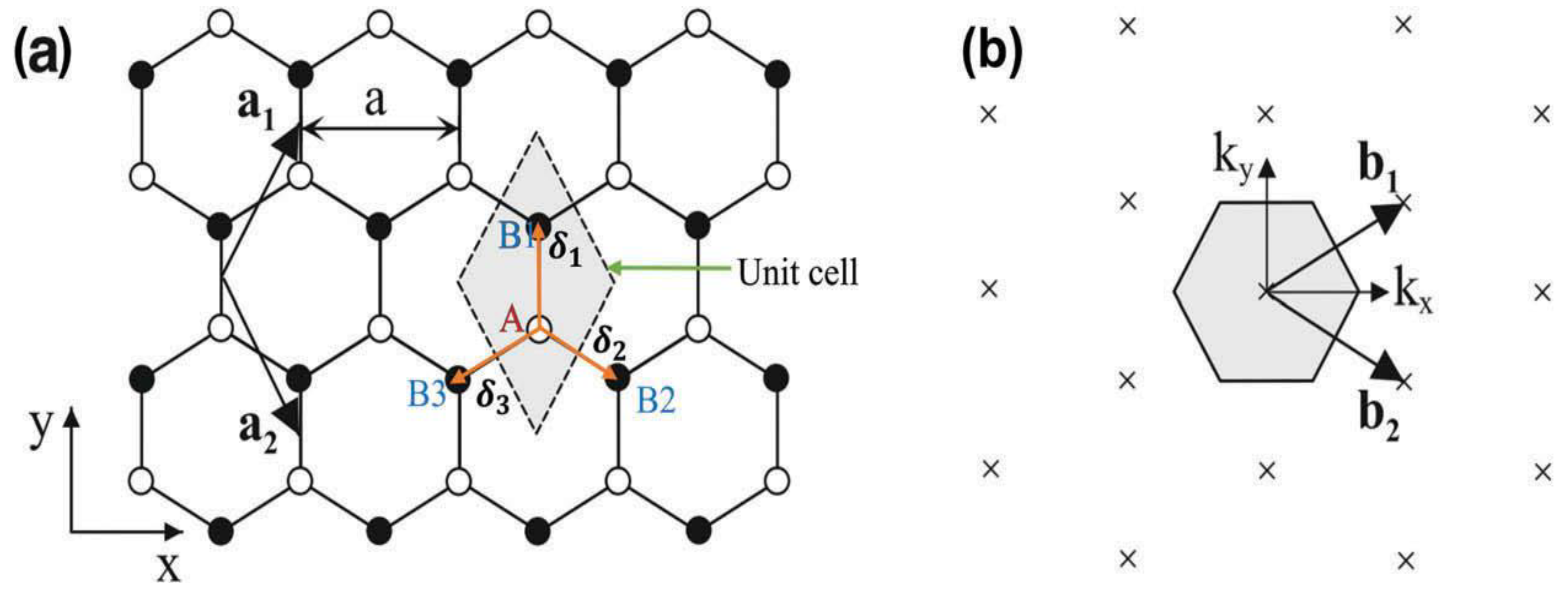
Two primitive vectors of a lattice are written in the hexagonal mesh of monolayer graphene, as shown in Figure 4a:
a 1 = a 2 ( 1 , 3 )   and   a 2 = a 2 ( 1 , 3 )
where a = 3 , and a 0 3 × 1.42 = 2.46   A is the lattice constant, which is the distance between unit cells. The position vector of atom B (1, 2, 3) relative to atom Ai is denoted as δ , and the three nearest neighbor vectors are real space given by:
δ = ( 0 , a 3 ) ,   δ = ( a 2 , a 2 3 )   and   δ = ( a 2 , a 2 3 )
It was noticed that | δ I | = | δ 2 | = | δ 3 | = a / 3 is the spacing of two neighbour carbon atoms; Figure 4 represents the reciprocal lattice of monolayer graphene. The primitive reciprocal lattice vectors b 1   and b 2   satisfy the conditions.
Whereas a 1 b 1 = a 2 b 2   = 2 Π ,
a 1 b 1 = a 2 b 2
Therefore,
b 1 = ( 2 Π / a , 2 Π 3     a )   and   b 1 = ( 2 Π a , 2 Π 3     a )
Usually, the electronic band structure of graphene can be calculated using the LACTO method, also called the tight-binding approach [43].

3. Preparation of Graphene Nanoparticles

Graphene synthesis is a process for manufacturing or extracting according to the product’s desired size, purity, and efflorescence. Different techniques to produce small graphic films were found at the earlier stage. Carbon was precipitated on metal surfaces by the late 1970s in the form of thin graphite layers [44,45]. Graphene is best explained as a single, delicate layer of graphite, the soft, flaky substance used in pencil lead. Graphite is an allotrope of the element carbon, which means that it has the same atoms, but it is arranged differently and gives the substance varied characteristics. For instance, diamond and graphite are both carbon sources, but they differ significantly. Graphite, although fragile, is exceptionally sturdy. In diamonds, however, the graphene atoms are structured hexagonally. It is interesting to note that when graphite is removed, it assumes specific miraculous properties. It is just a single atom, the first two-dimensional substance ever discovered. There have been ongoing efforts to develop high-quality graphene both for research and possible applications in large quantities. Graphene preparation methods can be divided into top-up and bottom-down methods [46].
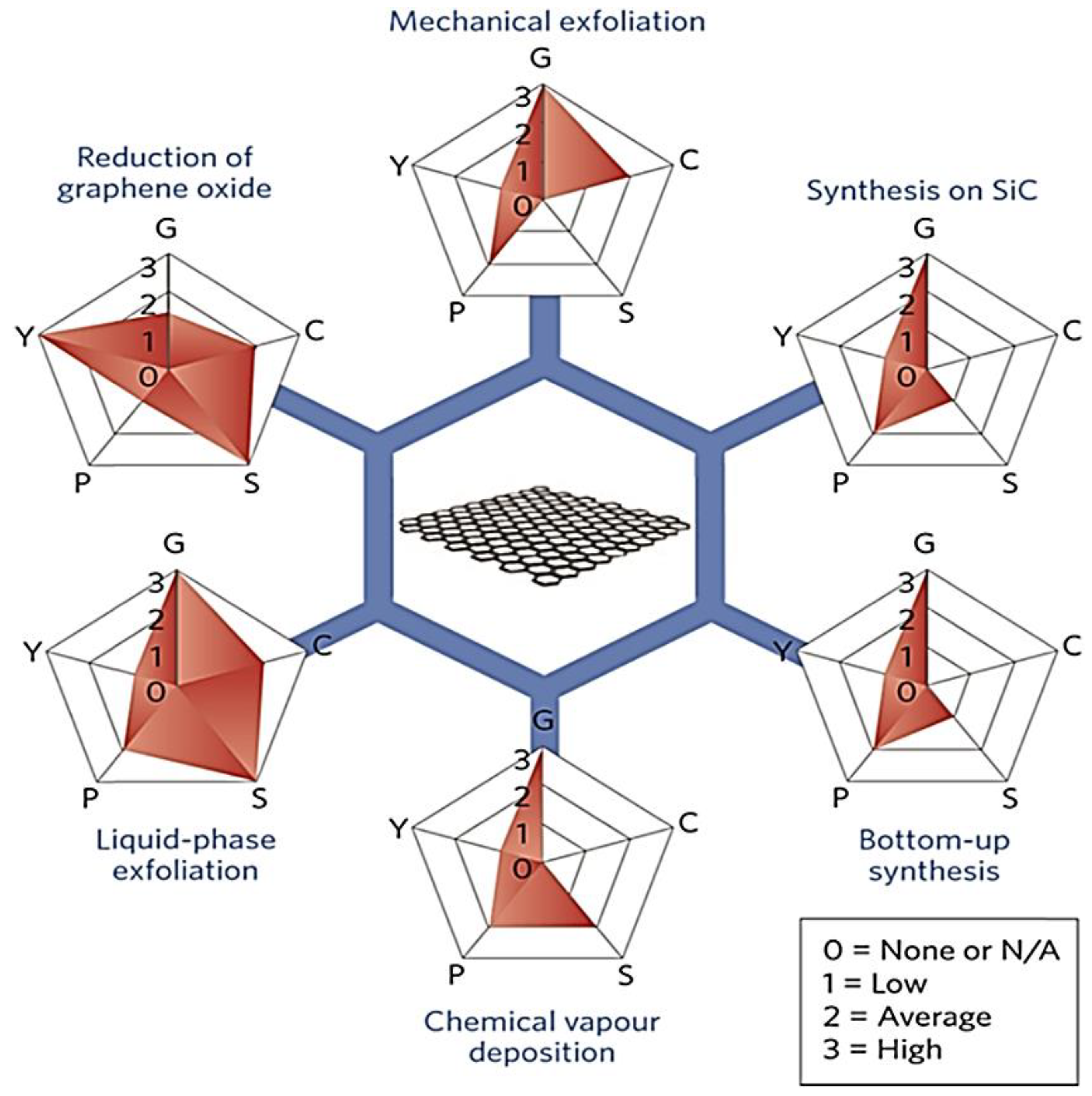
It is shown in Figure 5 [47] that smaller sheet size (<10 μm) requires the development of alternative approaches to generating graphene in sizes that are sufficiently large to cover practical applications in the transistor field. Mechanical exfoliation remains, to date, the process for transport measurements of high-quality single- and few-layer Gr sheets. However, many production methods allow high-quality Gr production in ever-larger areas and higher quality [48].
Although graphene preparation has been rapidly developed and advanced, low-cost methods of preparing large areas and monolayers are still not mature. High-purity graphene hinders large-scale graphene production and commercial uses. The challenge of graphene functional applications is still how to develop the flexible energy storage systems based on graphic, mobile, and wearable electronic devices and the functional composites and microelectronic components required to meet the demands of commercial applications. During the past few years, researchers have produced a short analysis and study of graphene preparation literature [49], illustrating the most common graphene production method, as indicated in Figure 6. In summary, basic graphene preparation is shown in Figure 7.

3.1. Top-Down Process

These top-down approaches are easier to implement on a wide scale and have lower costs, so it is no surprise that the most commercially available graphene uses top-down techniques. However, current world graphene production is not widespread due to the high cost of production. Therefore, it is still of utmost significance for successful commercialization and industrial acceptance to develop new methods and improvements in existing top-down processes [50]. Graphene production usually includes reduction or exfoliation with powdered graphite [51]. An example of a top-down synthesis procedure is the Nobel-prize-winning method of mechanical exfoliation developed by Novoselov et al. (2004). Home Scotch tape was used to mechanically peel SLG from a significantly oriented pyrolytic graphite with a lateral size of micrometres (HOPG) [52].

3.1.1. Mechanical Exfoliation

The rare and eminent procedure for extracting the graphene flocks of a single layer on preferred substrates is by mechanical exfoliation. It is the first known graphene synthesis method. This is a top-down nanotechnology technique whereby, on the circumference of the layered structural materials, there is longitudinal or transverse stress. Graphite is formed when weak Van der Waals forces pile the monoatomic graph layers together. The interlayer and layer-connecting energies are 3.34 A € per capita, and a 2 eV/nm2 €. A *300 nN/lm2 level of external strength is required for mechanical cleaning to separate one monoatomic layer from the graphite [53]. The graphite stacking of sheets results from a partially filled p orbital perpendicular to the sheet’s plane (Van der Waals forces involved). Exfoliation is the reverse of stacking; due to a weak bonding process and a considerable distance from the small lattice and stronger bonding on the hexagonal lattice plane, it takes the perpendicular direction [54].
The mechanical exfoliation process for graphite, known as the Scotch tape technology, developed in 2004, is usually considered only for adhering to some form of bulk graphite surface, such as removing the tape and then attaching the tape and residue to the substrate, usually silicon oxide. This tape is pulled off until the substrate is secured, and a final stage of exfoliation leaves behind flakes, preferably monolayer graphene, with randomly removed flakes of varying thickness [52]. However, Geim and Novoselov were more involved in the isolation of FLG. Their process began with a 1 mm HOPG oxygen plasma etch to produce tablets 5 μm deep from 20 μm to 2 mm square. The grated HOPG was then pushed over and plunged into a 1 μm wet Foton box on the surface of the glass. The resultant product was then heated and cured to consolidate the photoresist and pick up the mess. Phase 4 was completed by the cleared layer of HOPG, which remained above the table, leaving behind the collection of tablets in the photograph.
Phase 5 introduced the well-known “Scotch tape’’ process. The perpetual exploitation of Scotch tape was used to mechanically exfoliate the tablets strung in the photoresist to reduce the number of hopper layers held together by the weak Van der Waals forces. The mechanically exfoliated tablets were then placed in an acetone bath that released the flakes by dissolving the photoresist in acetone. The glass separated in the water and left graphic flakes floating in the acetone bath. In step 7, a 300 nm oxide layer silicone substrate (n+ doped) was immersed in the acetone bath and thin graphite flakes. The SiO2 substratum was removed and cleaned with water and propanol. Step 7 and step 8 were one stage in which the water and propanol in the solution were dipped, removed, and washed. Water helped in this process to catch the fine floors of the substratum. In the final phase, the substratum was placed in an ultrasound bath of propanol.
The further ultrasound purification process removed thicker flakes, and the graphite was thinner, possible FLG (~1 to 3 layers). In addition, the capillary and VDW forces supported by the material were observed to bind strongly to the SiO2 surface. Finally, the SiO2/graphene ensemble was extracted from the ultrasound bath, dried, and prepared to characterize and produce the unit [55,56]. This method is helpful for the physical study of large-scale graphene preparation [44].
This exfoliation method does not make it easy to obtain large amounts of graphene, not even in the absence of sustainable flakes. The challenge of this method is small, yet the graphene flakes must be found on the surface of the substratum, which is wide-ranging. The graphene is very high in quality with virtually no deficiencies. To produce FET devices, graphene made from these mechanical exfoliation techniques is used. However, for commercial-scale bulk production of flawless, high-purity graphene in the field of nanotechnology, the mechanical exfoliation method must be further enhanced [57]. The exfoliation method is shown in Figure 8.

3.1.2. Chemical Exfoliation

One of the most suitable methods for graphene syncretization is the chemical method. A colloidal suspension is a chemical method that modifies graphite and graphite intercalation compound graphene. Various types of papers, such as those on material science [59], polymer composites [60], energy storage materials [61], and transparent conductive electrodes [62], have already used chemical methods for the production of graphene. In 1860, graphene oxide was first manufactured, as reported by Brodie [63,64], Hummers [65], and Staudenmaier [66].
The two-step process includes chemical exfoliation. In the beginning, the interlayer Van der Waals force reduces the interlayer distance. Then, graphene intercalated compounds are formed (GICs) [67]. The mix of sulfuric and nitric acid intersperses the graphite to produce a higher-level GIC that may be exfoliated by fast-heating or dried-down polish microwave therapy to produce a substance commonly known as extended graphite [68]. The ultrasonic mixer used produces single-layer graphene in DMF/water (9:1) (dimethyl formamide). This explains how the spacing between the layers increases from 3.7 to 9.5 A/T. To oxidize the high density of functional groups and reduce them, graphite-like properties must be achieved. The chemical reduction with hydrazine monohydrate disperses single-layer graphene sheets [69]. Polycyclic aromatic hydrocarbons (PAHs) [69,70] have been used for the synthesis of graphene. Using a dendrite cell precursor transformed by cycloid hydrogenation and planarization produces small domains of graphene. A poly-dispersed, hyper-branched polyphenylene precursor gives larger flakes. The first was synthesized through oxidative cyclodehydrogenation with FeCl3 [71,72]. A variety of solvents were used to disperse graphene in perfluorinated aromatic solvents and ortho-dichlorobenzene [73] and even in low-boiling solvents, such as chloroform and isopropanol [74,75]; electrostatic attraction forces were observed between the HOPG and the Si substrate in the SiO2/Si substrates in graphene. Pulsed neodymium-doped yttrium aluminum grenade (Nd:YAG) laser exfoliation from HOPG was also used to prepare FG [76]. Graphite oxide reduction and thermal exfoliation also produce graphene, usually called graphene oxide reduction (RGO).

3.1.3. Reduction of Graphene Oxide

The experimentally designed model of graphene production from graphite is carried out by the chemical treatment process. A few routes were described by the author [77], as shown in Figure 9. The first step refers to the process, named oxidative exfoliation, wherein reduced graphene oxide is produced. The second step is liquid-phase chemical exfoliation of graphene by chemical and ultrasonication. Lastly, the route for preparing graphene is electrochemical exfoliation. One conventional method of preparing graphite in large quantities is the chemical reduction of graphite oxide. Graphite oxide (GO) is typically synthesized using oxidants, including concentrated sulphuric acid, nitric acid, and Brodie-based potassium permanganate, the Staudenmaier method, and the Hummers method through an oxidation process [78]. Reducing graphite oxide or graphite oxide into graphene is one of the low-cost methods used in large-scale graphene production. This method is currently the most popular method for producing graphene materials due to its possible scalability, high efficiency, and excellent dispersibility in different solvents, making processing easier for a variety of applications [79,80]. Sonication and graphene oxide (GO) reduction are other approaches to graphene production. H2 is added throughout the alkenes, coupled with nitrogen gas extrusion, which is used to reduce the excess NaBH4 as a reducing agent [81]. In the planning of RGO/graphene, 100 mg of as-arranged GO was scattered in 30 mL of every natural dissolvable (di-ethylene glycol (DEG), isopropanol (ISP), n-butanol (BA), n-hexylamine (HA), and ethyl acetic acid derivation (EA)) exclusively with the guide of gentle ultra-sonication for 1 h. A homogeneous arrangement was shaped, prompting a steady scattering proceeding to additional peeling of GO. The arrangements were then moved to a universally useful autoclave made of tempered steel (SS-316) furnished with a Teflon liner with a 30 mL limit. The autoclaves were kept at a temperature of 200 °C in a hot air boiler for 24 h and, afterward, permitted to chill to room temperature. The items were washed a few times with deionized water and ethanol, followed by centrifugation at 4000 rpm for 30 min. The last resultant items were saved for drying in a vacuum stove at 80 °C for 24 h, bringing about a fine, dark powder known as RGO/graphene [82].
Another way to synthesize large-scale graphene is by electronic reduction. The first single-layered graphene oxide flaking was established in 1962. The solution of graphite oxide was then sonicated so that GO nanoplatelets were formed. A hydrazine reduction agent was used to remove the oxygen group. However, there was no completion of the reduction process, leaving some oxygen. GO is helpful because, unlike graphite, its layers are hydrophilic. Therefore, sonication suspends GO in water reduction [83].

3.2. Bottom-Up Process

Most bulk graphene is produced with a top-down, exfoliating graphite approach which usually requires large quantities of solvent with high-energy mixing, shearing, sonication, or electrochemical processing [84]. As a result, a base-up amalgamation of great graphene is frequently limited to ultra-small sums whenever performed by substance fume testimony or by progressed engineered natural techniques, or it gives an imperfection-ridden structure whenever completed in mass arrangement [85,86].

3.2.1. Pyrolysis Process

The solvo heat technique was utilized as a compound blend of graphene in bottom-up measures. In this heat response, the molar proportion of sodium and ethanol was 1:1, kept in the shut vessel. The graphene sheets could be easily disconnected by the pluralization of sodium ethoxide utilizing sonication. This delivered graphene sheets with measurements of up to 10 µm. The translucent design, various layers, graphitic nature, and band structure were deep-rooted by SAED, TEM, and Raman spectroscopy [87].
Many-layered materials, including in situ templates and pre-synthesized templates, are used for the containment and guiding effects of graphene-like materials. To directly convert glucose to polycrystalline carbon sheets, a “matched” poly-domain graphene network with a domain size of 2 to 15 nm was used, a simple, synthetic process requiring neither catalytic nor solvent. The carbon assemblies showed high conductivity, a particular surface area, and the unforeseen process ability of solutions [88,89]. G-C3N4, boric acid, clays, and zeolites were the layered materials reported. The typical, layered structure is shown in g-C3N4. Dicyandiamide (DCDA), urea, and melamine could be calculated in the temperature interval of 500 °C to 600 °C and decomposed with NH3, C2N2+, C3N2+, and C3N3+ species at a temperature above 750 °C [90]. Thus, g-C3N4 can be used as a layered, graph-like carbon material synthesis slaughtering template. This method allows nitrogen doping with a concentration of around 3~5% in the resulting carbon nanosheet, even at high temperatures of 1000 °C. Monolayer and two-layer graphene may be formed with this method when the precursors are glucose and HMF. When, for instance, glucose with DCDA is heated together, the in-situ g-C3N4 formed at a temperature 600 °C can bind the intermediate formed aromatic carbon from glucose to its surface, thereby confining the intermediate carbon condensation in the g-C3N4 interlayer space. The process is demonstrated in Figure 10. The maximum temperature of g-C3N4, temperature thrombolysis, is then obtained at temperature 750 °C, while graphic sheets at high temperatures are obtained (e.g., 1000 °C). Urea g-C3N4 is cheap and easily available to prepare. The graph-like aerogenes/fibres with a hierarchical pore distribution resulted from a two-step pyrolysis of urea and cotton. Likewise, g-C3N4 was formed during pyrolysis at temperatures of approximately 500–600 °C, and carbon intermediates entered its interlayer space. The decomposition of g-C3N4 occurred at high temperatures of up to 900 °C, and carbon intermediates were transformed into N-doped graphene. A sophisticated, thin, layer-like, N-doped graphene structure was obtained when 5-hydroxymethyllfurfural was used as a carbon precursor and urea as a g-C3N4 precursor [91,92]. The guiding effect for graphene-like, N-doped carbon nanosheet formation in chitosan pyrolysis has also been reported as g-C3N4 sheets of urea. A high graphic nitrogen species and a high specific surface area have been found in the formative nanosheets.

3.2.2. Chemical Vapor Deposition (CVD)

Particularly in the synthesis of graphene with low carbon solid solubility (Cu) at high area thickness of uniformity and defect density, the reaction chamber pressure results in chemical vapor deposition (CVD) [94]. CVD is used to introduce a vapor from a gaseous reactant or liquid reactant consisting of a thin film element into the reaction chamber, which produces a chemical reaction on the substratum surface. It was later widely used in semiconductor films and is also a way of preparing graphene. CVD can produce large-scale preparation of high-purity graphene. However, graphene development is limited by the slow growth rate of the traditional CVD process [95]. CVD is the most regularly utilized thin film testimony strategy used to orchestrate CNTs. CVD is a different technique from the other CNT amalgamation strategies. The CVD strategy for creating CNTs enjoys the benefits of a high return of nanotubes and a lower temperature necessity (550 °C–1000 °C) which makes the interaction less expensive and more available for lab applications.
Moreover, the CVD strategy permits authority over the morphology and design of the CNTs created, and the development of adjusted nanotubes in an ideal way is conceivable. Be that as it may, the CVD technique has the drawback that the nanotubes are more fundamentally flawed than those created by laser dissipation or the curve release technique. Both curve release and laser vaporization are considered as short-response time (micro to milliseconds) and high-temperature measures (over 3000 K) [96].
On the other hand, catalytic CVD is an intermediate-temperature (700–1473 K) reaction of minutes to hours. Hydrocarbon or other carbon-bearing precursors are used in the presence of a catalyst in the CVD technique to produce CNTs and CNTs deposited on a substitute. In a CVD process, the temperature is usually less than 1200 °C. The advantage of this process is that CNTs with the required structure are produced by checking alignment, length, wall number, and diameter. Thus, CVD is generally seen as a low-cost process for manufacturing CNTs. The most common way to produce CNTs on a large scale is by using the fluidized bed process [97]. A typical fluidized bed scheme with a mass flow controller, gas distribution device, fluidized bed reactor, temperature controller, cold-trap system, and furnace is represented in Figure 11 [98].

3.2.3. Epitaxial Growth

Silicon carbide epitaxial graphene is one of the most promising, prominent graphene electronics candidates. Silicon-carbide-grown graphene has several advantages over metal substrates’ epitaxial graphene growth. One of the benefits is that no other electrical substratum must be transferred from the metal. SIC is a broad-band semiconductor “band to band” substratum widely used in the industry [99]. Hydrogen grazing removes scratches from polishing and oxides as a routine and leaves a surface with highly homogeneous atomic flat terraces. However, it is assumed that large amounts of graphene with a smoother graphitization surface can be obtained [100]. The relevance of the better graphene order of the pre-graphitization SiC surface has not been confirmed. The relationship between the initial morphology of the surface and sample quality has recently been discussed [101]. They observed SiC graph formation by Si sublimation in the atmosphere of argon (Ar) and found two kinds of monolayer graphene of various shapes. Large graphene sheets were noticed growing along with the three-layer SiC steps, whilst narrow graphene ribbons formed along the one-layer height surface. The dependence between the growth mechanisms and the initial morphology of the surface indicated H2 graphene formation. The results suggested that better graphene samples could be achieved by minimizing the number of single SiC steps with H2 etching [102].
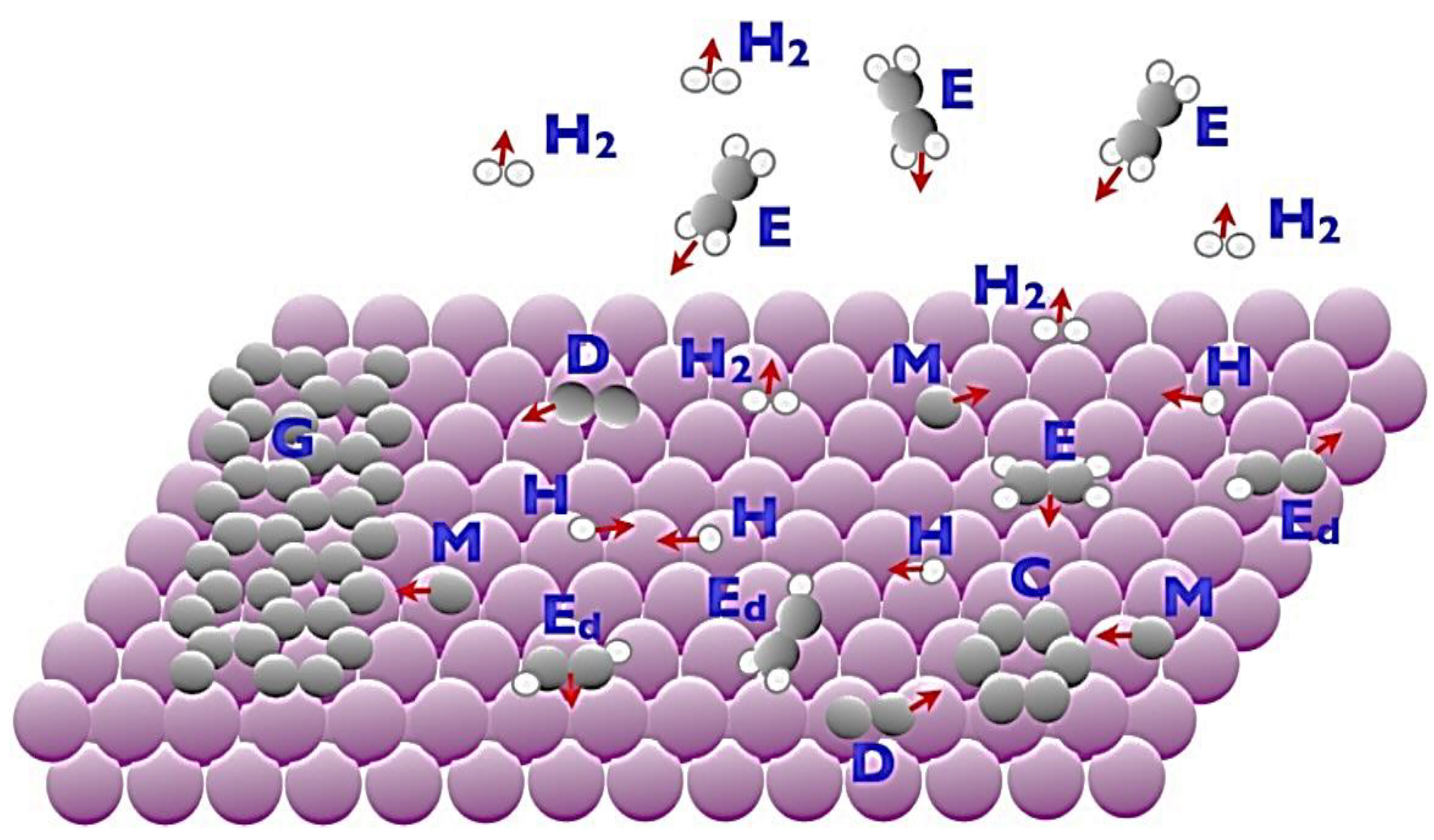
Typical epitaxy processes were illustrated by Tetlow et al. [95,103]. Some of these processes may need to be modified according to the material and the method of growth. First, starting with the filing. This is a testing process both in terms of the deposition and the deposited species. In the simplest case, the atomic (or molecular) component of the growing material is the deposited species, as this is often used in the growing thing of graphene, assuming that these are polyatomic precursors, E. In the latter, the kinetic of reaction is important, as certain surface sites can prevail in catalytic activity, and reaction products are to be desorbed from the surface (as shown by the hydrogen molecules H2). Even the atoms of the increasing material can desorb at high temperatures from the surface (not shown). The atomic species, M, diffuses on the surface after deposition and possibly decomposition kinetics. Even such an easy process can include difficult steps, such as exchanges, or even the forming of dimers, D, or larger C carbon clusters which migrate over the surface. The diffusing species concentration increases as deposition progresses and eventually reaches the level of G islands. This can occur through several processes. The colliding of two or more migratory species occurs in homogenous nucleation, binding then to an island. This island can be stable or break up depending on the temperature. The concentration of migratory species is eventually sufficient to induce the formation of the island, although many of these units are necessary. The rate of nucleation increases with the presence of a surface defect such as a vacancy, dislocation of the screws, or a previous step edge in heterogeneous nucleation, which is shown in Figure 11.

4. Properties of Graphene Nanoparticles

4.1. Electronics Properties

In each graphene grid, there are three bonds. The orbits of all carbon atoms are perpendicular to the hybridization of sp2 and form a de-located α bond, which passes through the whole graph [104,105]. Therefore, graphene has good conductivity and has a half-integer quantum Hall effect at room temperature, a bipolar electric field effect, superconductivity, a high carrier rate, and excellent electric properties. β electrons are free to move in the air. The electron is, therefore, free to move. Its mobility can range to 15,000 cm2/V at room temperature. Transporting the bandgap into the high power of the empty belt, an empty band with electrons following the conductive band, the price of the electron shortage after a positively charged space, is formed into holes. The electrons in the conduction band and the “trousers” in the valence band are known as electron–hole pairs which provide free transport of electrons and holes. They produce directional movement under external electric field action to form macro currents, electron conduction, and hole conduction [106].
Each unit of graphene has two atoms of carbon which cause two equal, tapered intersection points (K and K′) within each Brillion area, and energy is linearly associated with the wave vector at the intersection point [107,108]. During transport, the electrons in graphene do not become dispersed. As graphene electrons can move like zero mass particles, the electrons propagate at room temperature more quickly than any known conductor. Graphene electrons do not scatter as a consequence of gill or foreign electron defect in orbit; the graphene’s average free path can, therefore, reach 1 μm, and the general material’s average free path is within the range of the nanometer [109,110]. The graph bands are symmetrical for conduction and valence. Two kinds of electron and hole carrier are available. The ambitious electric field effects of the graph of one layer are shown in Figure 12A [111,112].

4.2. Mechanical Properties

One of the reasons graphene distinguishes itself both as an individual material and as a reinforcing agent in composites is its impressive mechanical properties. The cause of the extraordinary mechanical properties of graphene is the stability of the sp2 bonds which form the hexagonal grid and oppose different in-plan deformations [6]. First, by using the AFM nano-indentation (Figure 12A) and establishing the graphene as “the strongest material ever measured”, in their words, the mechanical properties of standing monolayer graphene were measured. To achieve both elastic properties and breaking stresses, the authors used the force-displacement response from the graphene membranes. The force-displacement curves (Figure 12B) were found to be insensitive to the tip radius, but, instead, they depended mainly on the radius of the tip and the membrane size [5,113].
A significant crack in the graphene membranes was introduced using a focused iron beam (FIB), and a breakdown after a load was applied was observed. An increasing crack life and a critical strain energy release rate (GC) decreased the fracture stress to 15.9 Jm−2, with the critical stress intensity factor (SCF) of 4.0 ± 0.6 MPa measuring the fracture tightness of graphene. From this and the like [114], monolayer graphene has been applied to springs that can be twisted with a magnetic field by up to 240% of their initial length. In the future, this idea could be extended to build high-performance mechanical metamaterials with a graph-based microscale [5,114].

4.3. Optical Properties

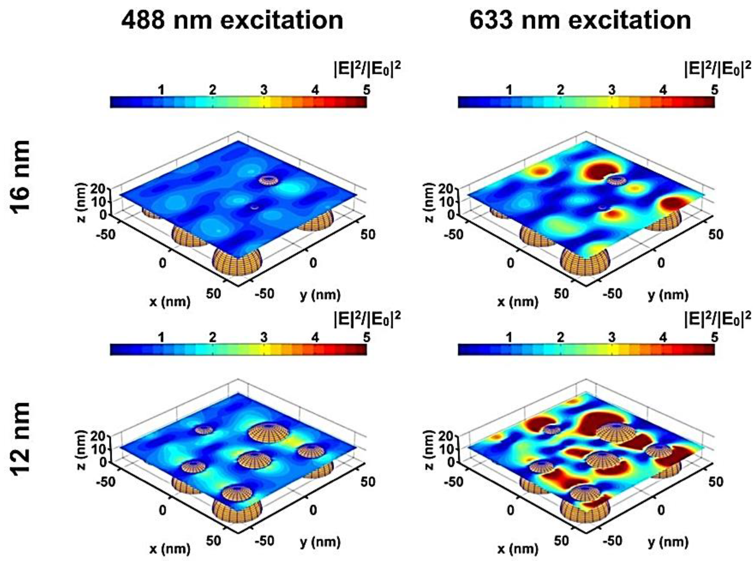
High-frequency conductance was shown to be equal to Π e 2 = 2 h from the infrared-through-visible spectrum ranges with Dirac closures in graphene [115,116]. For reconstructed clusters at different levels over the substratum level, the electric field enhancement |E|2/|E0|2 was shown for the two arousal wave lengths used in Raman experiments at different heights (12 and 16 nms, respectively) (488 nm and 633 nm, respectively) [117], as shown in Figure 13.
Figure 13. Distribution near field around the particles reconstructed. The intensity maps are shown at two different heights (12 nm and 16 nms) above the substratum level in the two excitement wavelengths (488 nm and 633 nm, respectively). Parallel to the x-axis lights, is the polarization. All plots are subject to the same intensity range. The field improvement in certain regions between two neighboring particles is well above a value of 5 for 633 nm excitation (hot spots).
Sustainability 14 12336 g013
A further reduction of mobility to 10,000–20,000 cm2/Vs [118] at room temperature was found in remote phonon interface dispersion from polar oxide substrates (such as SiO3) and inspired efforts to integrate graphs with alternative gate dielectrics. Graphene, for example, showed intrinsic mobility of about 500,000 cm2/V on ultra-flat boron nitride (BN) [119].
Due to these excellent optical properties of the graphene nanomaterial, it is also used in biological and medical science. Easy modification of the surface is a major feature, which makes GO more favorable than other carbon nanomaterials. GO can also be used for concurrent chemo- and photothermal treatment without adopting other pharmaceutical carriers thanks to its photothermal effect and drug transport capability [120].

4.4. Thermal Properties

The intrinsic thermal conductivity of graphene is extremely high. The small addition of liquid-phase exfoliated graphene can increase a composite materials’ thermal conductivity. The fillers can be electrically insulating and conductive to compounds with graphene and nanoparticles. As thermal interface materials, graphene composites are promising (TIMs). Graphene TIMs’ thermal conductivity reveals a low dependence on temperature—beneficial for applications in thermal management [121]. Empirically, graphene possesses a variety of unique properties such as (2630 m2g−1) 200 000 cm2v−1s−1 inherent mobility, a high Young’s modulus (~1.0 T), the thermal conductivity of high heat (~5000 Wm−1K−1), optical transmission capacity (~97.7%), and superb electrical conductivity. Graphene includes the extraordinary property of transporting heat energy. Therefore, scientists can now prepare free-standing sheets of graphene that have some of the highest electron mobilities of any inorganic semiconductor. The resistivity of ultraclean, suspended graphene is strongly temperature (T) dependent for 5 < T < 240 K. At T ~ 5 K transport is near ballistic in a device of ~2 μm dimension and mobility ~170,000 cm2/V s. At large carrier density n > 0.5 × 1011 cm−2, the resistivity increases with increasing temperature T and is linear above 50 K, suggesting carrier scattering from acoustic phonons. At T = 240 K, the mobility is ~120,000 cm2/V s, higher than in any known semiconductor. At the charge neutral point, a non-universal conductivity that decreases with decreasing T is observed, consistent with a density inhomogeneity <108  cm−2 [122,123].
In addition, graphene proved itself to be a prime candidate as a thermal paste for commercial usages, such as in next-generation thermal interface materials (TIMs), which are also used in solar cells to aid the heat removal process [124]. The π network in graphene emphasizes thermal efficacy and mechanical predominance. The thermal conductivity of graphene is reported to be 5 × 10³ Wm−1K−1, which is greater than diamond and graphite, and its Young’s modulus and intrinsic strength reach up to 1.0 TPa and 130 Gpa, respectively [6,125].
The solar absorption ability of nanofluids is important in volumetric solar collectors. One always expects that a larger absorption fraction of solar energy (AF) can be achieved through a minimum thickness and volume fraction of nanofluids. The thermal conductivity from the plane wave heat front can be expressed as K = ( L 2 S ) ( Δ P Δ T ) , where ∆P/∆T represents the change in heating power as a function of temperature, L is the distance from the center of the graphene to the heat sink, and S = h × W. For the radial heat wave case, K = χ G ( 1 2 h π ) ( δ ω δ P ) 1 , where δω/δP indicates the G peak position shift due to the heating power change. Consequently, the thermal conductivity can be expressed as below (Equation (5)):
K = χ G ( L 2 h W ) ( δ ω δ P ) 1
The excitation power dependence of the Raman G peak was measured for the suspended graphene layers. The increase in laser power induced an increase in the intensity and redshift of the G peak. The G peak position shift concerned the power change in the suspended graphene layers [126,127].
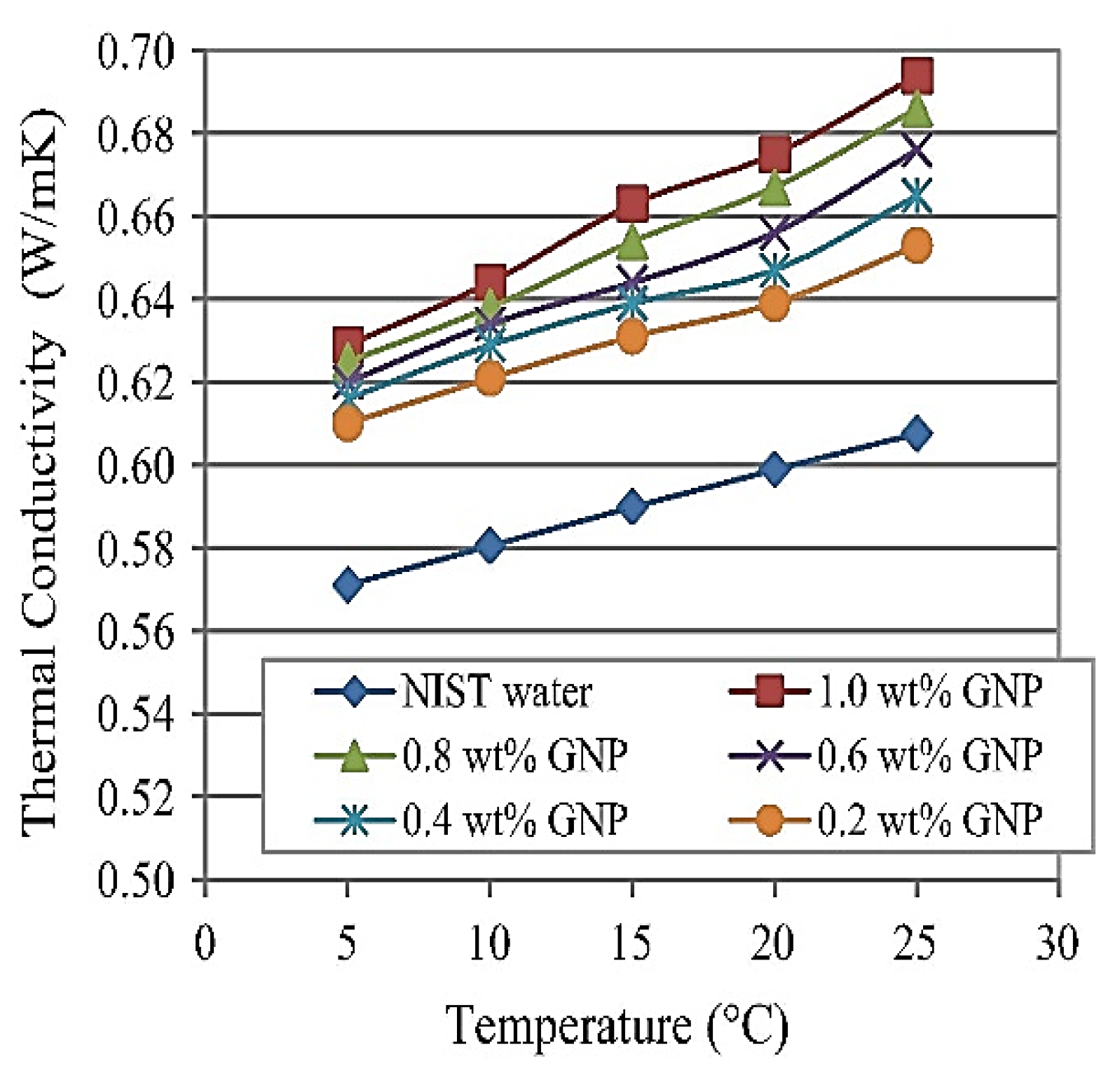
Figure 14 shows data on the thermal conductivity of GNP nanofluids with different concentrations and temperatures of nanoparticles. For comparison, NIST thermal conductivity values for water were obtained. The GNP nanofluid values of thermal conductivity rose linearly with the fluid temperature, as shown in Figure 9. For a maximum of 1 wt percent GNP of nanofluid at a temperature of 25 °C, the maximum thermal conductivity increase was 14.2%, while a minimum of 0.1 wt percent GNP of nanofluid was achieved at 5 °C [128].

4.5. Raman Spectroscopy of Graphene

Graphene is used for Raman spectroscopy, and a few review articles on the optical phonon spectrum and Raman graphene spectrum have been published [129]. The graphene spectra of Raman include an in-plan optical vibration (E 2 g de-generated zone center E mode) and a second-order zone border photometric vibration at 1580 cm−1 and a 2D peak at 2700 cm−1, respectively. The D peak is not present in defect-free graphene but exists with defeated graphene at 1350 cm−1 due to first-order area border phonons. The Raman spectra can be used to differentiate graphic quality and to determine by shape, width, and position of the peak of the 2D the number of n-layer graphs (for n up to 5) [130,131]. The so-called D, G, and 2D (also called G’), which have three main characteristics in their Raman spectrum, appear at approximately 1350, 1580, and 2700 cm−1 [132].
It is shown in Figure 15 that only defective samples are present in the first mode. The G model is a doubly degenerated first-order process involving transverse optical and longitudinal excitation in the center of the Brillouin zone. The other two are second order but double the resonant mode (as is easily observed, as in the G mode), with one optical transverse phone in the plane at the point K of the Brillouin zone and a D mode defect and two transverse optical phones in the plane at the point K for 2D mode (G’) [131,133].

5. Applications of Graphene Nanoparticles

5.1. Applications of Graphene in Energy

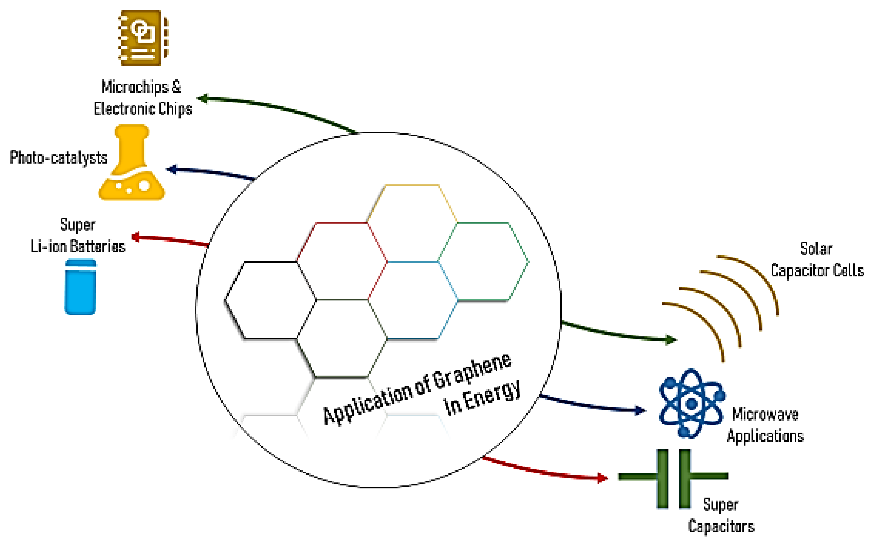
There are extensive applications of graphene-based nanomaterials in the energy-based sector of modern technology. Graphene-based energy storage systems have been developed for chemical, electrochemical, and electrical purposes. The commercial applications of graphene nanomaterials also include ongoing hydrogen storage systems, supercapacitors, and lithium batteries. Even though the exploration of the utilization of graphene for energy stockpiling started late, the unstable development of the examination directed in this space makes this mini review convenient [135]. Graphene is an alluring, delicate material for different applications because of its extraordinary and selective properties. The preparation and conservation of 2D graphene on every scale are trying because of graphene’s inborn inclination for layer restacking. The designs of three-dimensional, graphene-based nanomaterials (3D-GNMs) are protected while the process ability has been further developed alongside, giving upgraded qualities which show some remarkable benefits over 2D graphene [136]. Graphene–metal hybrid nanomaterials play a significant role in the world market as alternative electrical items that can serve fuel cells [137]. Figure 16 presents the use of graphene in different sectors, such as in microchips and electric chips, photocatalysts, super Li-ion batteries, solar capacitor cells, microwave applications, and super capacitors.

5.2. Graphene’s Applications in Medicine

Graphene is an alluring, delicate material for different applications because of its extraordinary and selective properties as in Figure 17. The preparation and conservation of 2D graphene on every scale are trying because of graphene’s inborn inclination for layer restacking. The designs of three-dimensional, graphene-based nanomaterials (3D-GNMs) are protected while the process ability has been further developed alongside, giving upgraded qualities which show some remarkable benefits over 2D graphene [138]. Due to its ultra-high surface area and easy surface functionalization, single-layered graphene has been intensively explored for drug and gene delivery. Utilizing their intrinsic, high, near-infrared absorbance, graphene and its derivatives were found to be excellent candidates for multimodal, imaging-guided, combined cancer photothermal and chemotherapies and/or photodynamic therapies. Then again, the drawn-out toxicological and metabolic practices of nano-graphene still have legitimacy, although they require more exertion before clinical use [139].
Graphene can likewise distinguish malignant cells in the beginning phases of the illness. Additionally, it can prevent them from filling any further in many kinds of disease by mediating the development of the growth or causing autophagy which prompts the demise of malignant cells [140]. Recent improvements exhibited that nanotechnology might offer new and powerful ways to deal with and battle malignancy. Until this point in time, various examinations gave accounts of the use of various nano-sized metals, metal oxides, and carbon-based nanoparticles for the therapy and imaging of malignancy. As of late, the two-dimensional carbon allotrope graphene has been displayed as a decent possibility for drug conveyance stages and hyperthermia because of its special physicochemical qualities, including simple functionalization and great biocompatibility, enormous surface-to-volume proportion, solid light-engrossing properties, and generally straightforward readiness [141]. Graphene and its subordinates have extraordinary physical and compound properties that make them promising vehicles for photothermal treatment (PTT)-based disease treatment as in Table 1. With natural, near-infrared (NIR) retention properties, graphene-based nanomaterials can be utilized for PTT and different therapeutics, especially in blended treatment, to provide fruitful, warm removal of malignant cells. In the new year, progress in graphene-based PTT has delivered proficient and effective cancer control through the nanomaterial foundational layout and distinctive functionalizations of graphene-determined nanocomposites. Graphene-based nano-systems display multifunctional properties that are valuable for PTT applications, including improvement of multimodalities, directed imaging, upgraded chemotherapy, and low-power, effective PTT for ideal, helpful effectiveness [142].
Graphene detects glucose by pulling it from the fluid present between the cells. This can not only end the painful methods of blood sugar monitoring but is also expected to increase the accuracy of the results [147,148,149,150,151,152,153,154,155,156,157,158,159]. Dialysis is a universal division measure in biochemical preparation and natural examination. Best-in-class dialysis layers include a somewhat thick polymer layer with convoluted pores and experience the ill effects of a low pace of dissemination, prompting very long interaction times (regularly a few days) and helpless selectivity, particularly in the 0–1000 Da sub-atomic weight range. Here, the manufacture of huge-region (cm2), nano-porous, molecularly flimsy films (NATMs) is accounted for by moving blended graphene utilizing versatile synthetic fume statement (CVD) to polycarbonate track-scratched upholds. After fixing discards presented during the move/taking care of interfacial polymerization, an effortless oxygen plasma draw is utilized to make size-particular pores (≤1 nm) in the CVD graphene [160]. Graphene is also used in bone and teeth implantation [161], tissue engineering, cell therapy, as performed by Shin et al. [77,151], biosensors, UV sensors [162,163], the brain [164], and birth control [165].

5.3. Graphene’s Applications in Electronics

Graphene can be utilized as a covering to further develop current touch evaluation for mobiles and tablets. It can likewise be utilized to make the hardware for our personal computers (PCs), making them unimaginably quick as in Figure 18. These are only two instances of how graphene can upgrade present gadgets. Graphene can likewise start the up-and-coming age of gadgets.
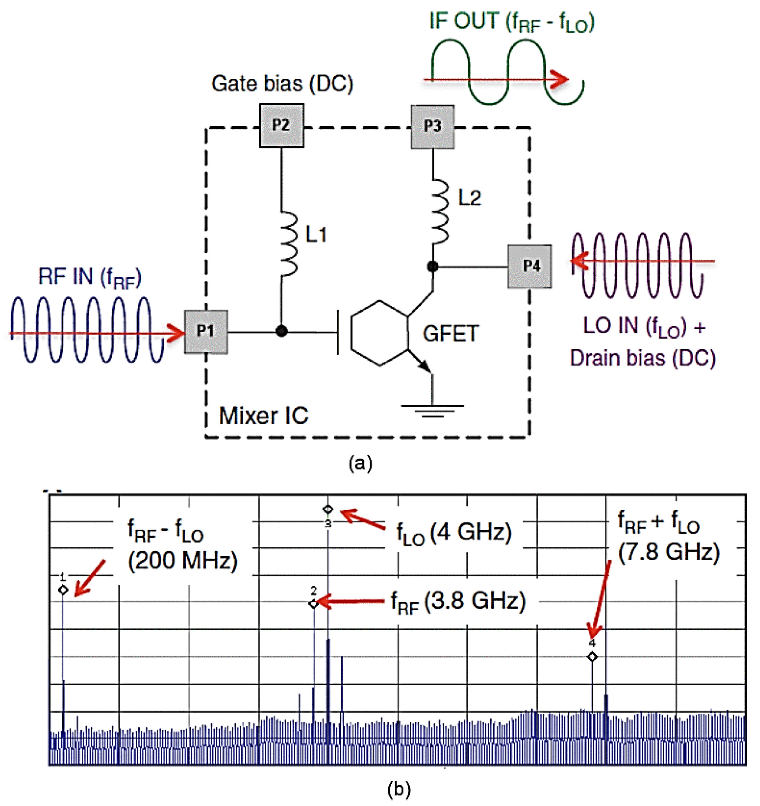
As mentioned above, graphene semiconductors with natural cut-off frequencies past 300 GHz have been shown in the enormous region of graphene materials. Be that as it may, concerning some other semiconductor advancements, it is fundamental to show the practicality of a solid mix of dynamic semiconductors with other inactive segments in Figure 19. Heterogeneous reconciliation of individual graphene semiconductors with outside, detached components has been shown as of late by different exploration gatherings [166]. An illustration of a solid mix of a graphene incorporated circuit (IC) is given by a recurrence blender created on a solitary SiC substrate utilizing wafer-scale handling [167].
Graphene conductive properties have been taken advantage of for some time in the field of natural photovoltaics and optoelectronics by established researchers around the world. A mixture bio-interface in which graphene is combined with photosensitive polymers and tried for its capacity to evoke light and set off neural action has been designed and portrayed. This opens the door to biomedical applications of graphene-based neuronal interfaces in the context of retinal implants [168]. To improve photoconversion in organic photovoltaic and photocatalytic devices, graphene has been extensively exploited [169].
The use of graphene and thin device geometry enables a capacitive touch sensor with good sensing capabilities in both contact and noncontact modes as in Table 2. Devices such as this can be attached to human body parts that are highly deformable, such as the forearms and palms. When multiple touch signals are recorded, this touch sensor can determine the distance and shape of the approaching objects before they are touched. For emerging, wearable electronics and robotics applications, this technology offers a convenient and immersive human–machine interface [170]. A high-resolution printed circuit can be created by inkjet printing on textiles, which reduces materials waste and natural resource consumption [171]. Further evidence of the effect of surface pre-treatment (NP1) on the conductivity of e-textiles can be seen in SEM images as in Figure 20. Figure 20 shows the interfacial interaction between fibers when hydrophobic NP1 is inkjet printed onto cotton fabrics (c, d) [172].

5.4. Other Applications of Graphene

Treatment of wastewater and groundwater polluted with human-created radionuclides, the most harmful of which are the transoceanic components, is a significant errand for tidying up heritage atomic offices. A recent mishap included the appearance of radionuclides in the Fukushima Daiichi Atomic Energy Environment in Japan whereby the water used to chill caused pollution. The requirement for successful treatment was underscored through its reactor centers as in Figure 21. Water was defiled with radionuclide techniques [173].
There are many usages of graphene nanoparticles in the food industry, especially in food packaging. This type of bio-nanocomposite has a variety of antimicrobial mechanisms, both physical and chemical. As main mechanisms of antimicrobial activity of graphene-based materials, researchers have suggested that membrane damage, oxidative stress, and electron transfer are the main mechanisms of action to some extent; pathogens’ structural damage may be caused by depolarization of membranes, which occurs when GO sheets come into direct contact with bacterial cells/fungal spores via cell wrapping and direct contact with the cell wall or membrane. Inhibition of microbial growth or death may be the result of it, affecting physiological metabolism processes [174]. The majority of the nanocarbon was tested for antibacterial properties against S. aureus and E. coli, but not against other bacteria in Figure 22. For example, its high efficacy against bacteria suggests that it has the potential to develop broad-spectrum antimicrobial activity against other pathogenic microorganisms. Biodegradable polymers–nanocarbon systems showed antifungal activity in a small number of studies, most of which focused on Aspergillus niger. The literature searches also turned up no studies on antiviral or antiprotozoal activity, temperature control, or removal properties [175].
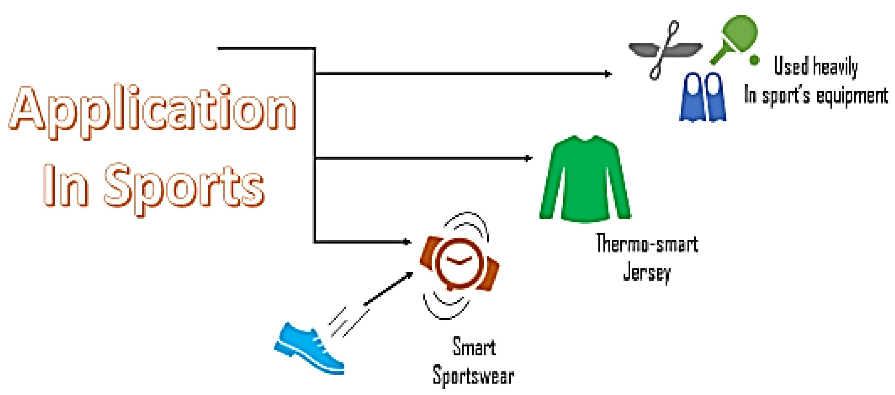
Using wearable fiber sensors, it is possible to monitor the human body’s basic movements. Typical soccer and basketball action was captured in a video. Using the fiber sensor, the movements of athletes could be accurately monitored by placing it on joints such as the shoulder, elbow, wrist, knee, ankle, and others. Each kick or shot was tracked to see how far it moves. Athletes’ movements could be improved based on the raw data collected from the sensors in various positions. Therefore, it was possible to accurately track and identify the subtle differences between athletes’ movements of the same joint [176]. Wearable graphene-coated composite fiber strain sensors were used to monitor human motion in sports such as basketball and soccer. They implemented the measurement and analysis of all the movement processes. In addition to accurate and vigorous movement, the data obtained were in line with the activities measured. A new type of fiber sensor will have broad and practical applications in sports monitoring and many other areas [177].
Powerful stage partition during the sorption cycle can likewise be guaranteed by choosing the communication conditions between the oxidized graphene suspension and the hydrophobic ligands as a reduced sorption material, which is coagulated in the ligand blend. This makes it especially essential to pick the strategy for extraction, including the conditions for the part blended during the sorption interaction. Because of suspension, the best interaction is achieved by adding oxidized graphene and ligand straightforwardly to the radionuclides to accomplish an extra sorbent and concentrate component in one phase. This empowers the extraction time to be abbreviated and sorption conditions to change effectively to guarantee that the component confinement is finished [84]. Graphene-based materials are receiving increased consideration as original materials for natural applications [178].

6. Future Trends

With the perpetual research and development of graphene nanomaterials for the latest applications, a lot of optimistic entrepreneurs and companies are eagerly penetrating the market. The sophisticated engineering and unparalleled characteristics of graphene nanoparticles have pushed them into numerous advanced technologies and applications. Sectors such as aeronautics, medicine, space, medicine, and sports, together with AI-based mechatronics, are the recipients dazzling with promising advanced innovations [179]. Some of the prime opportunities that are sneaking out are the following:
  • Graphene can conduct electrons nearly at light speed, making it a superconductive material. Researchers in the US have confirmed graphene to be an excellent conductor of heat as carbon nanotubes act as a good thermal conductor. Researchers are putting efforts into exploiting the thermal property of graphene to improve the efficiency of heat exchangers. Heat exchangers constructed from graphene coating show a better result in satellite cooling technology and, therefore, are highly appreciated by technologists. Hence, graphene nanocoated heat exchangers are certain to be commercialized in the near future;
  • Graphene possesses ultra-lightness and great mechanical strength. Researchers are optimistic about building solar sails weighing only a few pounds made from graphene which would help us to explore and learn more about solar systems;
  • The ultra-thin, lightweight feature has already accentuated its possibility and utilization in aeronautics and airspace. Airplane wings made from graphene particles resulted in a lower-weight structure which eventually improved thrust and take-off as well as fuel consumption. Researchers at University Central Lancashire successfully installed graphene-based wings on a drone named “Juno”, which is 17% lighter than carbon fiber. Now, there is a fine possibility to build a system integrated into the wings that could produce paints resulting in a reduction in radar footprints, as well as the establishment of invisible aircraft. EU’s white elephant, a zero-G aircraft whose heat exchangers are coated with graphene sheets, completed its parabolic flight in weightless conditions, enabling prospects in space;
  • Graphene oxide nanofilms impregnated on composite surfaces exhibit unprecedented aspects based on empirical tests and applications. GO nanofilms can be used as a heat shield capable of equalizing local heat formation, which enables it to be a stable flame retardant. Graphene’s coherent polymer matrix, combined with ceramics and epoxy resin, extinguishes the flame by delaying ignition and releasing exorbitant moisture;
  • Though nanomedicine is still in its embryonic stage, graphene is set to be incorporated with a variety of nanoparticles to assist in disease diagnosis and effective modern treatment. A significant amount of EU-backed funding has been disbursed into this material, and perpetual research projects concerning graphene make for a promising future. Antimicrobial applications in tissue engineering, neurological disorders, and genetic diseases are the newest opportunities in the field of medical science to alleviate the suffering of patients. It is believed that graphene nanocoated medical devices and apparels are safer to use and can effectively decelerate the spreading of lethal, antibiotic-resistant bugs. Researchers in Korea are optimistic about the attributes of graphene sheets capable of being used as a potential catalyst to support the growth of neural stem cells;
  • The sports and apparel industry is racing ahead towards superior performance and safer and much more comfortable clothing and accessories. Graphene-coated products are available in tennis, skiing, cycling; a lot of initiatives are being taken by sport product manufacturing heads [180]. The world is witnessing the evolution of sports equipment. Graphene’s unique characteristics, such as its higher strength-to-weight ratio and prolonged strength and durability, flexibility, and superior heat exchanging, improve the technical performance of sports accessories and attributes of sports products. Graphene, the game-changer, is ready to redeem the sports community on a large scale with its prominent commercial usage.

7. Conclusions

Graphene, the material from the future, emerged as an ambitious innovation in the world back in 2004. Despite being the prolific descendent of carbon, graphene’s bulk utilization and credibility in the industrial sectors and high-tech society, as well as in common usage, is yet to be proved. Though researchers have managed to yield graphene in flake form, engendering graphene sheets on a large, commercial basis is laborious and still to be developed. Consequently, graphene-based products and accessories are somewhat expensive and immature. Nevertheless, over the years, graphene’s astounding performance in various sectors has won hearts and competition in a grand fashion. Graphene, the honeycomb phenomenon, has the ultra edge to conquer the commercial sector because of its uniqueness in properties and outcomes. Its expanding opportunity and utility are raising the eyebrows of the researchers as well as the masses and encompassing new technology day by day. The graphene technology, along with its phenomenal characteristics, is set to reach the apex of its territory and, thus, take over the world.

Funding

This research was funded by University Malaysia Pahang, grant number FRGS/1/2022/TK10/UMP/02/35 RDU220124.

Institutional Review Board Statement

Not applicable.

Informed Consent Statement

Not applicable.

Acknowledgments

The authors are very thankful to University Malaysia Pahang for providing financial aid, FRGS/1/2022/TK10/UMP/02/35 RDU220124.

Conflicts of Interest

The authors declare no conflict of interest.

References

  1. Gomes, P.V.R.; Azeredo, N.F.B.; Garcia, L.M.S.; Zambiazi, P.J.; Morselli, G.R.; Ando, R.A.; Otubo, L.; Lazar, D.R.R.; de Souza, R.F.B.; Rodrigues, D.F.; et al. Layered graphene/hexagonal boron nitride nanosheets (Gr/h-BNNs) applied to the CO2 photoconversion into methanol. Appl. Mater. Today 2022, 29, 101605. [Google Scholar] [CrossRef]
  2. Alshamkhani, M.T.; Teong, L.K.; Putri, L.K.; Mohamed, A.R.; Lahijani, P.; Mohammadi, M. Effect of graphite exfoliation routes on the properties of exfoliated graphene and its photocatalytic applications. J. Environ. Chem. Eng. 2021, 9, 106506. [Google Scholar] [CrossRef]
  3. Balandin, A.A.; Ghosh, S.; Bao, W.; Calizo, I.; Teweldebrhan, D.; Miao, F.; Lau, C.N. Superior thermal conductivity of single-layer graphene. Nat. Mater. 2008, 8, 902–907. [Google Scholar] [CrossRef]
  4. Novoselov, K.S.; Geim, A.K.; Morozov, S.V.; Jiang, D.; Katsnelson, M.I.; Grigorieva, I.; Dubonos, S.; Firsov, A.A. Two-dimensional gas of massless Dirac fermions in graphene. Nature 2005, 438, 197–200. [Google Scholar] [CrossRef]
  5. Zhu, Y.; Murali, S.; Cai, W.; Li, X.; Suk, J.W.; Potts, J.R.; Ruoff, R.S. Graphene and graphene oxide: Synthesis, properties, and applications. Adv. Mater. 2010, 22, 3906–3924. [Google Scholar] [CrossRef]
  6. Lee, C.; Wei, X.; Kysar, J.W.; Hone, J.J. Measurement of the elastic properties and intrinsic strength of monolayer graphene. Science 2008, 321, 385–388. [Google Scholar] [CrossRef]
  7. Papageorgiou, D.G.; Kinloch, I.A.; Young, R.J.J. Graphene/elastomer nanocomposites. Carbon 2015, 95, 460–484. [Google Scholar] [CrossRef]
  8. Lin, Y.-M.; Jenkins, K.A.; Valdes-Garcia, A.; Small, J.P.; Farmer, D.B.; Avouris, P.J. Operation of graphene transistors at gigahertz frequencies. Nano Lett. 2009, 9, 422–426. [Google Scholar] [CrossRef]
  9. Bunch, J.S.; Van Der Zande, A.M.; Verbridge, S.S.; Frank, I.W.; Tanenbaum, D.M.; Parpia, J.M.; Craighead, H.G.; McEuen, P.L.J. Electromechanical resonators from graphene sheets. Science 2007, 315, 490–493. [Google Scholar] [CrossRef]
  10. Raju, A.P.A.; Lewis, A.; Derby, B.; Young, R.J.; Kinloch, I.A.; Zan, R.; Novoselov, K.S.J. Wide-area strain sensors based upon graphene-polymer composite coatings probed by Raman spectroscopy. Adv. Funct. Mater. 2014, 24, 2865–2874. [Google Scholar] [CrossRef]
  11. Yoo, J.J.; Balakrishnan, K.; Huang, J.; Meunier, V.; Sumpter, B.G.; Srivastava, A.; Conway, M.; Mohana Reddy, A.L.; Yu, J.; Vajtai, R.J.N.l. Ultrathin planar graphene supercapacitors. Nano Lett. 2011, 11, 1423–1427. [Google Scholar] [CrossRef]
  12. Patchkovskii, S.; John, S.T.; Yurchenko, S.N.; Zhechkov, L.; Heine, T.; Seifert, G.J. Graphene nanostructures as tunable storage media for molecular hydrogen. Proc. Natl. Acad. Sci. USA 2005, 102, 10439–10444. [Google Scholar] [CrossRef]
  13. Farhana, K.; Kadirgama, K.; Subramonian, S.; Ramasamy, D.; Samykano, M.; Mahamude, A.S.F. Applications of Graphene Nanomaterials in Energy Storage—A State-of-Art Short Review. In Proceedings of the International Conference on Mechanical Engineering Research 2021, 26–27 October 2021; Springer: Singapore, 2023; pp. 595–609. [Google Scholar]
  14. Wang, X.; Zhi, L.; Müllen, K.J. Transparent, conductive graphene electrodes for dye-sensitized solar cells. Nano Lett. 2008, 8, 323–327. [Google Scholar] [CrossRef]
  15. Miao, X.; Tongay, S.; Petterson, M.K.; Berke, K.; Rinzler, A.G.; Appleton, B.R.; Hebard, A.F.J. High efficiency graphene solar cells by chemical doping. Nano Lett. 2012, 12, 2745–2750. [Google Scholar] [CrossRef]
  16. Farhana, K.; Kadirgama, K.; Rahman, M.; Ramasamy, D.; Noor, M.; Najafi, G.; Samykano, M.; Mahamude, A.J. Improvement in the performance of solar collectors with nanofluids—A state-of-the-art review. Nano-Struct. Nano-Objects 2019, 18, 100276. [Google Scholar] [CrossRef]
  17. Jia, X.; Campos-Delgado, J.; Terrones, M.; Meunier, V.; Dresselhaus, M.S.J. Graphene edges: A review of their fabrication and characterization. Nanoscale 2011, 3, 86–95. [Google Scholar] [CrossRef]
  18. Shen, J.; Zhu, Y.; Yang, X.; Li, C.J. Graphene quantum dots: Emergent nanolights for bioimaging, sensors, catalysis and photovoltaic devices. Chem. Commun. 2012, 48, 3686–3699. [Google Scholar] [CrossRef]
  19. Xu, Y.; Sheng, K.; Li, C.; Shi, G. Self-assembled graphene hydrogel via a one-step hydrothermal process. ACS Nano 2010, 4, 4324–4330. [Google Scholar] [CrossRef]
  20. Xue, Y.; Liu, J.; Chen, H.; Wang, R.; Li, D.; Qu, J.; Dai, L. Nitrogen-doped graphene foams as metal-free counter electrodes in high-performance dye-sensitized solar cells. Angew. Chem. Int. Ed. 2012, 51, 12124–12127. [Google Scholar] [CrossRef]
  21. Wu, Z.-S.; Sun, Y.; Tan, Y.-Z.; Yang, S.; Feng, X.; Müllen, K. Three-dimensional graphene-based macro-and mesoporous frameworks for high-performance electrochemical capacitive energy storage. J. Am. Chem. Soc. 2012, 134, 19532–19535. [Google Scholar] [CrossRef]
  22. Mahamude, A.S.F.; Harun, W.S.W.; Kadirgama, K.; Ramasamy, D.; Farhana, K.; Salih, K.; Yusaf, T. Experimental Study on the Efficiency Improvement of Flat Plate Solar Collectors Using Hybrid Nanofluids Graphene/Waste Cotton. Energies 2022, 15, 2309. [Google Scholar] [CrossRef]
  23. Young, R.J.; Kinloch, I.A.; Gong, L.; Novoselov, K.S. The mechanics of graphene nanocomposites: A review. Compos. Sci. Technol. 2012, 72, 1459–1476. [Google Scholar] [CrossRef]
  24. Das, S.; Kim, M.; Lee, J.-W.; Choi, W.J. Synthesis, properties, and applications of 2-D materials: A comprehensive review. Crit. Rev. Solid State Mater. Sci. 2014, 39, 231–252. [Google Scholar] [CrossRef]
  25. Mahamude, A.S.F.; Harun, W.S.W.; Kadirgama, K.; Farhana, K.; Ramasamy, D.; Samylingam, L.; Aslfattahi, N. Thermal performance of nanomaterial in solar collector: State-of-play for graphene. J. Energy Storage 2021, 42, 103022. [Google Scholar] [CrossRef]
  26. Farhana, K.; Kadirgama, K.; Noor, M.; Rahman, M.; Ramasamy, D.; Mahamude, A. CFD modelling of different properties of nanofluids in header and riser tube of flat plate solar collector. IOP Conf. Series: Mater. Sci. Eng. 2019, 469, 012041. [Google Scholar] [CrossRef]
  27. Choi, W.; Lahiri, I.; Seelaboyina, R.; Kang, Y.S.J. Synthesis of graphene and its applications: A review. Crit. Rev. Solid State Mater. Sci. 2010, 35, 52–71. [Google Scholar] [CrossRef]
  28. Wang, C.; Astruc, D. Recent developments of metallic nanoparticle-graphene nanocatalysts. Prog. Mater. Sci. 2018, 94, 306–383. [Google Scholar] [CrossRef]
  29. Mahamude, A.S.F.; Harun, W.S.W.; Kadirgama, K.; Farhana, K.; Ramasamy, D. Numerical Studies of Graphene Hybrid Nanofluids in Flat Plate Solar Collector. In Proceedings of the 2021 International Congress of Advanced Technology and Engineering (ICOTEN), Taiz, Yemen, 4–5 July 2021; pp. 1–6. [Google Scholar]
  30. Kadirgama, G.; Bin Razman, M.I.; Ramasamy, D.; Kadirgama, K.; Farhana, K. Graphene as an Alternative Additive in Automotive Cooling System. In Proceedings of the International Conference on Mechanical Engineering Research, ICMER 2021, 26–27 October 2021; Springer: Singapore, 2023; pp. 13–35. [Google Scholar]
  31. Zhang, X.; Rajaraman, B.R.; Liu, H.; Ramakrishna, S.J. Graphene’s potential in materials science and engineering. Rsc Adv. 2014, 4, 28987–29011. [Google Scholar] [CrossRef]
  32. Chen, J.; Zhang, M.; Gu, P.; Yan, Z.; Tang, C.; Lv, B.; Wang, X.; Yi, Z.; Zhu, M. Broadband, wide-incident-angle, and polarization-insensitive high-efficiency absorption of monolayer graphene with nearly 100% modulation depth at communication wavelength. Results Phys. 2022, 40, 105833. [Google Scholar] [CrossRef]
  33. Yi, L.; Li, C. Enhanced absorption and electrical modulation of graphene based on the parity-time symmetry optical structure. Chin. Opt. Lett. 2022, 20, 022201. [Google Scholar] [CrossRef]
  34. Teng, Y.; Tong, S.; Zhang, M. Secondary-Transferring Graphene Electrode for Stable FOLED. Nanoscale Res. Lett. 2018, 13, 352. [Google Scholar] [CrossRef] [PubMed]
  35. Liu, B.; Tang, C.; Chen, J.; Xie, N.; Zheng, L.; Wang, S. Tri-band absorption enhancement in monolayer graphene in visible spectrum due to multiple plasmon resonances in metal–insulator–metal nanostructure. Appl. Phys. Express 2018, 11, 072201. [Google Scholar] [CrossRef]
  36. Liu, B.; Tang, C.; Chen, J.; Wang, Q.; Pei, M.; Tang, H. Dual-band light absorption enhancement of monolayer graphene from surface plasmon polaritons and magnetic dipole resonances in metamaterials. Opt. Express 2017, 25, 12061–12068. [Google Scholar] [CrossRef] [PubMed]
  37. Hiura, H.; Ebbesen, T.; Fujita, J.; Tanigaki, K.; Takada, T.J. Role of sp 3 defect structures in graphite and carbon nanotubes. Nature 1994, 367, 148–151. [Google Scholar] [CrossRef]
  38. Yang, G.; Li, L.; Lee, W.B.; Ng, M.C.J. Structure of graphene and its disorders: A review. Sci. Technol. Adv. Mater. 2018, 19, 613–648. [Google Scholar] [CrossRef]
  39. Cooper, D.R.; D’Anjou, B.; Ghattamaneni, N.; Harack, B.; Hilke, M.; Horth, A.; Majlis, N.; Massicotte, M.; Vandsburger, L.; Whiteway, E.J. Experimental review of graphene. Int. Sch. Res. Not. 2012, 2012, 258. [Google Scholar] [CrossRef]
  40. McCann, E. Electronic properties of monolayer and bilayer graphene. In Graphene Nanoelectronics; Springer: Berlin/Heidelberg, Germany, 2011; pp. 237–275. [Google Scholar]
  41. Wallace, P.R.J. The band theory of graphite. Phys. Rev. 1947, 71, 622. [Google Scholar] [CrossRef]
  42. Eizenberg, M.; Blakely, J.J. Carbon monolayer phase condensation on Ni (111). Surf. Sci. 1979, 82, 228–236. [Google Scholar] [CrossRef]
  43. Eizenberg, M.; Blakely, J.J. Carbon interaction with nickel surfaces: Monolayer formation and structural stability. J. Chem. Phys. 1979, 71, 3467–3477. [Google Scholar] [CrossRef]
  44. Singh, K.; Ohlan, A.; Dhawan, S.J. Polymer-graphene nanocomposites: Preparation, characterization, properties, and applications. Nanocompos.-New Trends Dev. 2012, 37–72. [Google Scholar] [CrossRef] [Green Version]
  45. Bonaccorso, F.; Lombardo, A.; Hasan, T.; Sun, Z.; Colombo, L.; Ferrari, A.C.J. Production and processing of graphene and 2d crystals. Mater. Today 2012, 15, 564–589. [Google Scholar] [CrossRef]
  46. Kitko, K.E.; Zhang, Q.J. Graphene-based nanomaterials: From production to integration with modern tools in neuroscience. Front. Syst. Neurosci. 2019, 13, 26. [Google Scholar] [CrossRef]
  47. Raccichini, R.; Varzi, A.; Passerini, S.; Scrosati, B.J. The role of graphene for electrochemical energy storage. Nat. Mater. 2015, 14, 271–279. [Google Scholar] [CrossRef]
  48. Kumar, N.; Salehiyan, R.; Chauke, V.; Botlhoko, O.J.; Setshedi, K.; Scriba, M.; Masukume, M.; Ray, S.S.J. Top-down synthesis of graphene: A comprehensive review. FlatChem 2021, 27, 100224. [Google Scholar] [CrossRef]
  49. Lim, J.Y.; Mubarak, N.; Abdullah, E.; Nizamuddin, S.; Khalid, M.J. Recent trends in the synthesis of graphene and graphene oxide based nanomaterials for removal of heavy metals—A review. J. Ind. Eng. Chem. 2018, 66, 29–44. [Google Scholar] [CrossRef]
  50. Novoselov, K.S.; Geim, A.K.; Morozov, S.V.; Jiang, D.-E.; Zhang, Y.; Dubonos, S.V.; Grigorieva, I.V.; Firsov, A.A.J. Electric field effect in atomically thin carbon films. Science 2004, 306, 666–669. [Google Scholar] [CrossRef]
  51. Zhang, Y.; Small, J.P.; Pontius, W.V.; Kim, P.J. Fabrication and electric-field-dependent transport measurements of mesoscopic graphite devices. Appl. Phys. Lett. 2005, 86, 073104. [Google Scholar] [CrossRef]
  52. Rao, C.; Maitra, U.; Matte, H.S.S. Synthesis, characterization, and selected properties of graphene. Acc. Chem. Res. 2013, 46, 149–159. [Google Scholar] [CrossRef]
  53. Hader, G.G.J. Synthesis, Modelling Characterization of 2D Materials Their Heterostructures; Elsevier: Amsterdam, The Netherlands, 2020; Volume 181. [Google Scholar]
  54. Casiraghi, C.; Hartschuh, A.; Lidorikis, E.; Qian, H.; Harutyunyan, H.; Gokus, T.; Novoselov, K.S.; Ferrari, A.J. Rayleigh imaging of graphene and graphene layers. Nano Lett. 2007, 7, 2711–2717. [Google Scholar] [CrossRef]
  55. Teng, C.; Xie, D.; Wang, J.; Yang, Z.; Ren, G.; Zhu, Y.J. Ultrahigh conductive graphene paper based on ball-milling exfoliated graphene. Adv. Funct. Mater. 2017, 27, 1700240. [Google Scholar] [CrossRef]
  56. Bhuyan, M.S.A.; Uddin, M.N.; Islam, M.M.; Bipasha, F.A.; Hossain, S.S.J. Synthesis of graphene. Int. Nano Lett. 2016, 6, 65–83. [Google Scholar] [CrossRef]
  57. Chen, J.; Liu, B.; Gao, X.J. Thermal properties of graphene-based polymer composite materials: A molecular dynamics study. Results Phys. 2020, 16, 102974. [Google Scholar] [CrossRef]
  58. Xiao, J.; Zhan, H.; Wang, X.; Xu, Z.-Q.; Xiong, Z.; Zhang, K.; Simon, G.P.; Liu, J.Z.; Li, D.J. Electrolyte gating in graphene-based supercapacitors and its use for probing nanoconfined charging dynamics. Nat. Nanotechnol. 2020, 15, 683–689. [Google Scholar] [CrossRef]
  59. Samantaray, M.R.; Mondal, A.K.; Murugadoss, G.; Pitchaimuthu, S.; Das, S.; Bahru, R.; Mohamed, M.A.J. Synergetic effects of hybrid carbon nanostructured counter electrodes for dye-sensitized solar cells: A review. Materials 2020, 13, 2779. [Google Scholar] [CrossRef] [PubMed]
  60. Dzyazko, Y.S.; Volfkovich, Y.M.; Chaban, M.O. Composites Containing Inorganic Ion Exchangers and Graphene Oxide: Hydrophilic–Hydrophobic and Sorption Properties. In Nanomaterials and Nanocomposites, Nanostructure Surfaces, and Their Applications; Springer: Berlin/Heidelberg, Germany, 2021; pp. 93–110. [Google Scholar]
  61. Alkhouzaam, A.; Qiblawey, H.; Khraisheh, M.; Atieh, M.; Al-Ghouti, M.J. Synthesis of graphene oxides particle of high oxidation degree using a modified Hummers method. Ceram. Int. 2020, 46, 23997–24007. [Google Scholar] [CrossRef]
  62. Ma, Y.; Zheng, Y.; Zhu, Y.J. Towards industrialization of graphene oxide. Sci. China Mater. 2020, 63, 1861–1869. [Google Scholar] [CrossRef]
  63. Sharotri, N.; Rana, A.K.; Thakur, N.; Dogra, S.; Dhiman, N. Fundamental of Graphene Nanocomposites. In Handbook of Polymer and Ceramic Nanotechnology; Springer: Cham, Switzerland, 2021; pp. 1161–1184. [Google Scholar]
  64. Guohua, C.J. Exfoliation of graphite flake and its nanocomposites. Carbon 2003, 41, 579. [Google Scholar]
  65. Park, S.; An, J.; Jung, I.; Piner, R.D.; An, S.J.; Li, X.; Velamakanni, A.; Ruoff, R.S.J. Colloidal suspensions of highly reduced graphene oxide in a wide variety of organic solvents. Nano Lett. 2009, 9, 1593–1597. [Google Scholar] [CrossRef]
  66. Cai, J.; Ruffieux, P.; Jaafar, R.; Bieri, M.; Braun, T.; Blankenburg, S.; Muoth, M.; Seitsonen, A.P.; Saleh, M.; Feng, X.J. Atomically precise bottom-up fabrication of graphene nanoribbons. Nature 2010, 466, 470–473. [Google Scholar] [CrossRef]
  67. Li, L.-S.; Yan, X.J. Colloidal graphene quantum dots. J. Phys. Chem. Lett. 2010, 1, 2572–2576. [Google Scholar] [CrossRef]
  68. Zhi, L.; Müllen, K.J. A bottom-up approach from molecular nanographenes to unconventional carbon materials. J. Mater. Chem. 2008, 18, 1472–1484. [Google Scholar] [CrossRef]
  69. O’Neill, A.; Khan, U.; Nirmalraj, P.N.; Boland, J.; Coleman, J.N.J. Graphene dispersion and exfoliation in low boiling point solvents. J. Phys. Chem. C 2011, 115, 5422–5428. [Google Scholar] [CrossRef]
  70. Hamilton, C.E.; Lomeda, J.R.; Sun, Z.; Tour, J.M.; Barron, A.R.J. High-yield organic dispersions of unfunctionalized graphene. Nano Lett. 2009, 9, 3460–3462. [Google Scholar] [CrossRef] [PubMed]
  71. Hernandez, Y.; Lotya, M.; Rickard, D.; Bergin, S.D.; Coleman, J.N.J. Measurement of multicomponent solubility parameters for graphene facilitates solvent discovery. ACS Publ. 2010, 26, 3208–3213. [Google Scholar] [CrossRef]
  72. Qian, M.; Zhou, Y.S.; Gao, Y.; Park, J.B.; Feng, T.; Huang, S.M.; Sun, Z.; Jiang, L.; Lu, Y.F.J. Formation of graphene sheets through laser exfoliation of highly ordered pyrolytic graphite. Appl. Phys. Lett. 2011, 98, 173108. [Google Scholar] [CrossRef]
  73. Parvez, K.; Yang, S.; Feng, X.; Müllen, K.J. Exfoliation of graphene via wet chemical routes. Synth. Met. 2015, 210, 123–132. [Google Scholar] [CrossRef]
  74. William, S.; Hummers, J.; Offeman, R.E.J.J. Preparation of graphitic oxide. Am. Chem. Soc. 1958, 80, 1339. [Google Scholar]
  75. Tung, V.C.; Allen, M.J.; Yang, Y.; Kaner, R.B.J. High-throughput solution processing of large-scale graphene. Nat. Nanotechnol. 2009, 4, 25–29. [Google Scholar] [CrossRef]
  76. Li, D.; Müller, M.B.; Gilje, S.; Kaner, R.B.; Wallace, G.G. Processable aqueous dispersions of graphene nanosheets. Nat. Nanotechnol. 2008, 3, 101–105. [Google Scholar] [CrossRef]
  77. Shin, H.J.; Kim, K.K.; Benayad, A.; Yoon, S.M.; Park, H.K.; Jung, I.S.; Jin, M.H.; Jeong, H.K.; Kim, J.M.; Choi, J.Y.J. Efficient reduction of graphite oxide by sodium borohydride and its effect on electrical conductance. Adv. Funct. Mater. 2009, 19, 1987–1992. [Google Scholar] [CrossRef]
  78. Lellala, K.; Namratha, K.; Byrappa, K.J. Ultrasonication assisted mild solvothermal synthesis and morphology study of few-layered graphene by colloidal suspensions of pristine graphene oxide. Microporous Mesoporous Mater. 2016, 226, 522–529. [Google Scholar] [CrossRef]
  79. Eda, G.; Fanchini, G.; Chhowalla, M.J. Large-area ultrathin films of reduced graphene oxide as a transparent and flexible electronic material. Nat. Nanotechnol. 2008, 3, 270–274. [Google Scholar] [CrossRef] [PubMed]
  80. Costes, L.; Laoutid, F.; Brohez, S.; Dubois, P.J.M.S.; Reports, E.R. Bio-based flame retardants: When nature meets fire protection. Mater. Sci. Eng. R Rep. 2017, 117, 1–25. [Google Scholar] [CrossRef]
  81. Choucair, M.; Thordarson, P.; Stride, J.A.J. Gram-scale production of graphene based on solvothermal synthesis and sonication. Nat. Nanotechnol. 2009, 4, 30–33. [Google Scholar] [CrossRef] [PubMed]
  82. Li, X.H.; Kurasch, S.; Kaiser, U.; Antonietti, M. Synthesis of monolayer-patched graphene from glucose. Wiley Online Libr. 2012, 51, 9689–9692. [Google Scholar] [CrossRef] [PubMed]
  83. Huang, B.; Xia, M.; Qiu, J.; Xie, Z.J. Biomass Derived Graphene-Like Carbons for Electrocatalytic Oxygen Reduction Reaction. ChemNanoMat 2019, 5, 682–689. [Google Scholar] [CrossRef]
  84. Liu, J.; Zhang, T.; Wang, Z.; Dawson, G.; Chen, W.J. Simple pyrolysis of urea into graphitic carbon nitride with recyclable adsorption and photocatalytic activity. J. Mater. Chem. 2011, 21, 14398–14401. [Google Scholar] [CrossRef]
  85. Liu, Q.; Duan, Y.; Zhao, Q.; Pan, F.; Zhang, B.; Zhang, J.J.L. Direct synthesis of nitrogen-doped carbon nanosheets with high surface area and excellent oxygen reduction performance. ACS Publ. 2014, 30, 8238–8245. [Google Scholar] [CrossRef]
  86. Wen, G.; Gu, Q.; Liu, Y.; Schlögl, R.; Wang, C.; Tian, Z.; Su, D.S.J. Biomass-Derived Graphene-like Carbon: Efficient Metal-Free Carbocatalysts for Epoxidation. Angew. Chem. Int. Ed. 2018, 57, 16898–16902. [Google Scholar] [CrossRef]
  87. Bhaviripudi, S.; Jia, X.; Dresselhaus, M.S.; Kong, J.J. Role of kinetic factors in chemical vapor deposition synthesis of uniform large area graphene using copper catalyst. Nano Lett. 2010, 10, 4128–4133. [Google Scholar] [CrossRef]
  88. Ren, S.; Rong, P.; Yu, Q.J. Preparations, properties and applications of graphene in functional devices: A concise review. Ceram. Int. 2018, 44, 11940–11955. [Google Scholar]
  89. Journet, C.; Maser, W.; Bernier, P.; Loiseau, A.; de La Chapelle, M.L.; Lefrant, D.S.; Deniard, P.; Lee, R.; Fischer, J.J. Large-scale production of single-walled carbon nanotubes by the electric-arc technique. Nature 1997, 388, 756–758. [Google Scholar] [CrossRef]
  90. Shukrullah, S.; Mohamed, N.; Shaharun, M.; Naz, M.J. Mass production of carbon nanotubes using fluidized bed reactor: A short review. Trends Appl. Sci. Res. 2014, 9, 121. [Google Scholar] [CrossRef] [Green Version]
  91. Hu, Y.; Ruan, M.; Guo, Z.; Dong, R.; Palmer, J.; Hankinson, J.; Berger, C.; De Heer, W.A.J. Structured epitaxial graphene: Growth and properties. J. Phys. D Appl. Phys. 2012, 45, 154010. [Google Scholar]
  92. Charrier, A.; Coati, A.; Argunova, T.; Thibaudau, F.; Garreau, Y.; Pinchaux, R.; Forbeaux, I.; Debever, J.-M.; Sauvage-Simkin, M.; Themlin, J.-M.J. Solid-state decomposition of silicon carbide for growing ultra-thin heteroepitaxial graphite films. J. Appl. Phys. 2002, 92, 2479–2484. [Google Scholar] [CrossRef]
  93. Howell, S.W.; Biedermann, L.B.; Ohta, T.; Ross III, A.J.; Beechem, I.; Edwin, T.; Pan, W.; Trotter, D.C. Characterization of Devices Fabricated from Electrostatically Transferred Graphene: Comparison with Epitaxial Based Devices; Sandia National Lab. (SNL-NM): Albuquerque, NM, USA, 2010.
  94. Yu, X.; Hwang, C.; Jozwiak, C.M.; Köhl, A.; Schmid, A.K.; Lanzara, A.; Phenomena, R. New synthesis method for the growth of epitaxial graphene. J. Electron Spectrosc. Relat. Phenom. 2011, 184, 100–106. [Google Scholar] [CrossRef]
  95. Tetlow, H.; De Boer, J.P.; Ford, I.; Vvedensky, D.; Coraux, J.; Kantorovich, L.J. Growth of epitaxial graphene: Theory and experiment. Phys. Rep. 2014, 542, 195–295. [Google Scholar] [CrossRef]
  96. Wang, L.; Meric, I.; Huang, P.; Gao, Q.; Gao, Y.; Tran, H.; Taniguchi, T.; Watanabe, K.; Campos, L.; Muller, D.J. One-dimensional electrical contact to a two-dimensional material. Science 2013, 342, 614–617. [Google Scholar]
  97. Yan, J.-A.; Ruan, W.; Chou, M.J. Electron-phonon interactions for optical-phonon modes in few-layer graphene: First-principles calculations. Phys. Rev. B 2009, 79, 115443. [Google Scholar]
  98. Ando, T.J. The electronic properties of graphene and carbon nanotubes. NPG Asia Mater. 2009, 1, 17–21. [Google Scholar] [CrossRef]
  99. Castro Neto, A.H.; Guinea, F.; Peres, N.M.R.; Novoselov, K.S.; Geim, A.K.J. The electronic properties of graphene. Rev. Mod. Phys. 2009, 81, 109–162. [Google Scholar] [CrossRef]
  100. Du, X.; Skachko, I.; Barker, A.; Andrei, E.Y.J. Approaching ballistic transport in suspended graphene. Nat. Nanotechnol. 2008, 3, 491–495. [Google Scholar] [CrossRef] [PubMed]
  101. Miao, F.; Wijeratne, S.; Zhang, Y.; Coskun, U.; Bao, W.; Lau, C.J. Phase-coherent transport in graphene quantum billiards. Science 2007, 317, 1530–1533. [Google Scholar] [CrossRef]
  102. Geim, A.K.; Novoselov, K.S. The rise of graphene. In Nanoscience and Technology: A Collection of Reviews from Nature Journals; World Scientific: Singapore, 2010; pp. 11–19. [Google Scholar]
  103. Zhang, Y.; Tan, Y.-W.; Stormer, H.L.; Kim, P.J. Experimental observation of the quantum Hall effect and Berry’s phase in graphene. Nature 2005, 438, 201–204. [Google Scholar] [CrossRef] [PubMed]
  104. Papageorgiou, D.G.; Kinloch, I.A.; Young, R.J. Mechanical properties of graphene and graphene-based nanocomposites. Prog. Mater. Sci. 2017, 90, 75–127. [Google Scholar] [CrossRef]
  105. Blees, M.K.; Barnard, A.W.; Rose, P.A.; Roberts, S.P.; McGill, K.L.; Huang, P.Y.; Ruyack, A.R.; Kevek, J.W.; Kobrin, B.; Muller, D.A.J. Graphene kirigami. Nature 2015, 524, 204–207. [Google Scholar] [CrossRef]
  106. Peres, N.; Guinea, F.; Neto, A.C.J. Electronic properties of disordered two-dimensional carbon. Phys. Rev. B 2006, 73, 125411. [Google Scholar] [CrossRef]
  107. Gusynin, V.; Sharapov, S.; Carbotte, J.J. Unusual microwave response of Dirac quasiparticles in graphene. Phys. Rev. Lett. 2006, 96, 256802. [Google Scholar] [CrossRef]
  108. Osváth, Z.; Deák, A.; Kertész, K.; Molnár, G.; Vértesy, G.; Zámbó, D.; Hwang, C.; Biró, L.P.J. The structure and properties of graphene on gold nanoparticles. Nanoscale 2015, 7, 5503–5509. [Google Scholar] [CrossRef]
  109. Chen, J.-H.; Jang, C.; Xiao, S.; Ishigami, M.; Fuhrer, M.S.J. Intrinsic and extrinsic performance limits of graphene devices on SiO2. Nat. Nanotechnol. 2008, 3, 206–209. [Google Scholar] [CrossRef]
  110. Jariwala, D.; Sangwan, V.K.; Lauhon, L.J.; Marks, T.J.; Hersam, M.C.J. Carbon nanomaterials for electronics, optoelectronics, photovoltaics, and sensing. Chem. Soc. Rev. 2013, 42, 2824–2860. [Google Scholar] [CrossRef] [PubMed]
  111. Li, J.-L.; Tang, B.; Yuan, B.; Sun, L.; Wang, X.-G.J. A review of optical imaging and therapy using nanosized graphene and graphene oxide. Biomaterials 2013, 34, 9519–9534. [Google Scholar] [CrossRef] [PubMed]
  112. Shahil, K.M.; Balandin, A.A.J. Thermal properties of graphene and multilayer graphene: Applications in thermal interface materials. Solid State Commun. 2012, 152, 1331–1340. [Google Scholar] [CrossRef]
  113. Bolotin, K.I.; Sikes, K.J.; Hone, J.; Stormer, H.; Kim, P.J. Temperature-dependent transport in suspended graphene. Phys. Rev. Lett. 2008, 101, 096802. [Google Scholar] [CrossRef] [PubMed]
  114. Naghibi, S.; Kargar, F.; Wright, D.; Huang, C.Y.T.; Mohammadzadeh, A.; Barani, Z.; Salgado, R.; Balandin, A.A. Noncuring graphene thermal interface materials for advanced electronics. Adv. Electron. Mater. 2020, 6, 1901303. [Google Scholar] [CrossRef]
  115. Ranjbartoreh, A.R.; Wang, B.; Shen, X.; Wang, G.J. Advanced mechanical properties of graphene paper. J. Appl. Phys. 2011, 109, 014306. [Google Scholar] [CrossRef]
  116. Rhee, K.Y. Electronic and Thermal Properties of Graphene. Nanomaterials 2020, 10, 926. [Google Scholar] [CrossRef]
  117. Sang, M.; Shin, J.; Kim, K.; Yu, K.J.J. Electronic and thermal properties of graphene and recent advances in graphene based electronics applications. Nanomaterials 2019, 9, 374. [Google Scholar] [CrossRef]
  118. Wang, Y.; Al-Saaidi, H.A.I.; Kong, M.; Alvarado, J.L.J. Thermophysical performance of graphene based aqueous nanofluids. Int. J. Heat Mass Transf. 2018, 119, 408–417. [Google Scholar] [CrossRef]
  119. Nagyte, V.; Kelly, D.J.; Felten, A.; Picardi, G.; Shin, Y.; Alieva, A.; Worsley, R.E.; Parvez, K.; Dehm, S.; Krupke, R.J. Raman fingerprints of graphene produced by anodic electrochemical exfoliation. Nano Lett. 2020, 20, 3411–3419. [Google Scholar] [CrossRef]
  120. Malard, L.; Pimenta, M.A.; Dresselhaus, G.; Dresselhaus, M.J. Raman spectroscopy in graphene. Phys. Rep. 2009, 473, 51–87. [Google Scholar] [CrossRef]
  121. Ferrari, A.C.; Meyer, J.C.; Scardaci, V.; Casiraghi, C.; Lazzeri, M.; Mauri, F.; Piscanec, S.; Jiang, D.; Novoselov, K.S.; Roth, S.J. Raman spectrum of graphene and graphene layers. Phys. Rev. Lett. 2006, 97, 187401. [Google Scholar] [CrossRef] [PubMed]
  122. Ferrari, A.C.J. Raman spectroscopy of graphene and graphite: Disorder, electron–phonon coupling, doping and nonadiabatic effects. Solid State Commun. 2007, 143, 47–57. [Google Scholar] [CrossRef]
  123. Li, X.; Cai, W.; Colombo, L.; Ruoff, R.S.J. Evolution of graphene growth on Ni and Cu by carbon isotope labeling. Nano Lett. 2009, 9, 4268–4272. [Google Scholar] [CrossRef] [PubMed]
  124. Pumera, M.J.E.; Science, E. Graphene-based nanomaterials for energy storage. Energy Environ. Sci. 2011, 4, 668–674. [Google Scholar] [CrossRef]
  125. Thiruppathi, A.R.; Sidhureddy, B.; Boateng, E.; Soldatov, D.V.; Chen, A.J. Synthesis and electrochemical study of three-dimensional graphene-based nanomaterials for energy applications. Nanomaterials 2020, 10, 1295. [Google Scholar] [CrossRef]
  126. Huang, C.; Li, C.; Shi, G.J. Graphene based catalysts. Energy Environ. Sci. 2012, 5, 8848–8868. [Google Scholar] [CrossRef]
  127. Priyadarsini, S.; Mohanty, S.; Mukherjee, S.; Basu, S.; Mishra, M.J. Graphene and graphene oxide as nanomaterials for medicine and biology application. J. Nanostruct. Chem. 2018, 8, 123–137. [Google Scholar] [CrossRef]
  128. Yang, K.; Feng, L.; Liu, Z.J. The advancing uses of nano-graphene in drug delivery. Expert Opin. Drug Deliv. 2015, 12, 601–612. [Google Scholar] [CrossRef]
  129. Orecchioni, M.; Cabizza, R.; Bianco, A.; Delogu, L.G.J. Graphene as cancer theranostic tool: Progress and future challenges. Theranostics 2015, 5, 710. [Google Scholar] [CrossRef]
  130. Eskiizmir, G.; Baskın, Y.; Yapıcı, K. Graphene-based nanomaterials in cancer treatment and diagnosis. In Fullerens, Graphenes and Nanotubes; Elsevier: Amsterdam, The Netherlands, 2018; pp. 331–374. [Google Scholar]
  131. Chen, Y.-W.; Su, Y.-L.; Hu, S.-H.; Chen, S.-Y.J. Functionalized graphene nanocomposites for enhancing photothermal therapy in tumor treatment. Adv. Drug Deliv. Rev. 2016, 105, 190–204. [Google Scholar] [CrossRef] [PubMed]
  132. Li, J.; Lyv, Z.; Li, Y.; Liu, H.; Wang, J.; Zhan, W.; Chen, H.; Chen, H.; Li, X.J. A theranostic prodrug delivery system based on Pt (IV) conjugated nano-graphene oxide with synergistic effect to enhance the therapeutic efficacy of Pt drug. Biomaterials 2015, 51, 12–21. [Google Scholar] [CrossRef] [PubMed]
  133. Wang, X.; Sun, X.; Lao, J.; He, H.; Cheng, T.; Wang, M.; Wang, S.; Huang, F.J. Multifunctional graphene quantum dots for simultaneous targeted cellular imaging and drug delivery. Colloids Surf. B Biointerfaces 2014, 122, 638–644. [Google Scholar] [CrossRef] [PubMed]
  134. Wang, H.; Gu, W.; Xiao, N.; Ye, L.; Xu, Q.J. Chlorotoxin-conjugated graphene oxide for targeted delivery of an anticancer drug. Int. J. Nanomed. 2014, 9, 1433. [Google Scholar]
  135. Wang, Y.; Polavarapu, L.; Liz-Marzán, L.M.J. Reduced graphene oxide-supported gold nanostars for improved SERS sensing and drug delivery. ACS Appl. Mater. Interfaces 2014, 6, 21798–21805. [Google Scholar] [CrossRef] [PubMed]
  136. Wang, C.; Chen, B.; Zou, M.; Cheng, G.J. Cyclic RGD-modified chitosan/graphene oxide polymers for drug delivery and cellular imaging. Colloids Surf. B Biointerfaces 2014, 122, 332–340. [Google Scholar] [CrossRef]
  137. Song, E.; Han, W.; Li, C.; Cheng, D.; Li, L.; Liu, L.; Zhu, G.; Song, Y.; Tan, W.J. Hyaluronic acid-decorated graphene oxide nanohybrids as nanocarriers for targeted and pH-responsive anticancer drug delivery. ACS Appl. Mater. Interfaces 2014, 6, 11882–11890. [Google Scholar] [CrossRef]
  138. Ou, J.; Wang, F.; Huang, Y.; Li, D.; Jiang, Y.; Qin, Q.-H.; Stachurski, Z.; Tricoli, A.; Zhang, T.J.C.; Biointerfaces, S.B. Fabrication and cyto-compatibility of Fe3O4/SiO2/graphene–CdTe QDs/CS nanocomposites for drug delivery. Colloids Surf. B Biointerface 2014, 117, 466–472. [Google Scholar] [CrossRef]
  139. Liu, X.; Ma, D.; Tang, H.; Tan, L.; Xie, Q.; Zhang, Y.; Ma, M.; Yao, S.J. Polyamidoamine dendrimer and oleic acid-functionalized graphene as biocompatible and efficient gene delivery vectors. ACS Appl. Mater. Interfaces 2014, 6, 8173–8183. [Google Scholar] [CrossRef]
  140. Kim, H.; Kim, W.J.J. Photothermally controlled gene delivery by reduced graphene oxide–polyethylenimine nanocomposite. Small 2014, 10, 117–126. [Google Scholar] [CrossRef]
  141. You, P.; Yang, Y.; Wang, M.; Huang, X.; Huang, X.J. Graphene oxide-based nanocarriers for cancer imaging and drug delivery. Curr. Pharm. Des. 2015, 21, 3215–3222. [Google Scholar] [CrossRef] [PubMed]
  142. Rahmanian, N.; Hamishehkar, H.; Dolatabadi, J.E.N.; Arsalani, N. Nano graphene oxide: A novel carrier for oral delivery of flavonoids. Biointerfaces 2014, 123, 331–338. [Google Scholar] [CrossRef] [PubMed]
  143. Liu, K.; Wang, Y.; Li, H.; Duan, Y. A facile one-pot synthesis of starch functionalized graphene as nano-carrier for pH sensitive and starch-mediated drug delivery. Colloids Surf. B Biointerfaces 2015, 128, 86–93. [Google Scholar] [CrossRef] [PubMed]
  144. Yang, Y.; Shi, H.; Wang, Y.; Shi, B.; Guo, L.; Wu, D.; Yang, S.; Wu, H.J. Graphene oxide/manganese ferrite nanohybrids for magnetic resonance imaging, photothermal therapy and drug delivery. J. Biomater. Appl. 2016, 30, 810–822. [Google Scholar] [CrossRef] [PubMed]
  145. Wu, J.; Chen, A.; Qin, M.; Huang, R.; Zhang, G.; Xue, B.; Wei, J.; Li, Y.; Cao, Y.; Wang, W.J.N. Hierarchical construction of a mechanically stable peptide–graphene oxide hybrid hydrogel for drug delivery and pulsatile triggered release in vivo. Nanoscale 2015, 7, 1655–1660. [Google Scholar] [CrossRef]
  146. Tang, Y.; Hu, H.; Zhang, M.G.; Song, J.; Nie, L.; Wang, S.; Niu, G.; Huang, P.; Lu, G.; Chen, X.J.N. An aptamer-targeting photoresponsive drug delivery system using “off–on” graphene oxide wrapped mesoporous silica nanoparticles. Nanoscale 2015, 7, 6304–6310. [Google Scholar] [CrossRef]
  147. Lee, H.; Choi, T.K.; Lee, Y.B.; Cho, H.R.; Ghaffari, R.; Wang, L.; Choi, H.J.; Chung, T.D.; Lu, N.; Hyeon, T.J. A graphene-based electrochemical device with thermoresponsive microneedles for diabetes monitoring and therapy. Nat. Nanotechnol. 2016, 11, 566–572. [Google Scholar] [CrossRef]
  148. Kafi, M.A.; Paul, A.; Vilouras, A.; Hosseini, E.S.; Dahiya, R.S.J. Chitosan-graphene oxide-based ultra-thin and flexible sensor for diabetic wound monitoring. IEEE Sens. J. 2019, 20, 6794–6801. [Google Scholar] [CrossRef]
  149. Kidambi, P.R.; Jang, D.; Idrobo, J.C.; Boutilier, M.S.; Wang, L.; Kong, J.; Karnik, R.J. Nanoporous atomically thin graphene membranes for desalting and dialysis applications. Adv. Mater. 2017, 29, 1700277. [Google Scholar] [CrossRef]
  150. Nishida, E.; Miyaji, H.; Kato, A.; Takita, H.; Iwanaga, T.; Momose, T.; Ogawa, K.; Murakami, S.; Sugaya, T.; Kawanami, M.J. Graphene oxide scaffold accelerates cellular proliferative response and alveolar bone healing of tooth extraction socket. Int. J. Nanomed. 2016, 11, 2265. [Google Scholar]
  151. Shin, S.R.; Li, Y.-C.; Jang, H.L.; Khoshakhlagh, P.; Akbari, M.; Nasajpour, A.; Zhang, Y.S.; Tamayol, A.; Khademhosseini, A. Graphene-based materials for tissue engineering. Adv. Drug Deliv. Rev. 2016, 105, 255–274. [Google Scholar] [CrossRef] [PubMed]
  152. Yun, J.; Lim, Y.; Lee, H.; Lee, G.; Park, H.; Hong, S.Y.; Jin, S.W.; Lee, Y.H.; Lee, S.S.; Ha, J.S.J. A Patterned Graphene/ZnO UV Sensor Driven by Integrated Asymmetric Micro-Supercapacitors on a Liquid Metal Patterned Foldable Paper. Adv. Funct. Mater. 2017, 27, 1700135. [Google Scholar] [CrossRef]
  153. Masvidal-Codina, E.; Illa, X.; Dasilva, M.; Calia, A.B.; Dragojević, T.; Vidal-Rosas, E.E.; Prats-Alfonso, E.; Martínez-Aguilar, J.; Jose, M.; Garcia-Cortadella, R.J. High-resolution mapping of infraslow cortical brain activity enabled by graphene microtransistors. Nat. Mater. 2019, 18, 280–288. [Google Scholar] [CrossRef] [PubMed]
  154. Lehtinen, O.; Kurasch, S.; Krasheninnikov, A.; Kaiser, U.J. Atomic scale study of the life cycle of a dislocation in graphene from birth to annihilation. Nat. Commun. 2013, 4, 2098. [Google Scholar] [CrossRef] [PubMed]
  155. Yang, X.; Liu, G.; Balandin, A.A.; Mohanram, K.J. Triple-mode single-transistor graphene amplifier and its applications. ACS Nano 2010, 4, 5532–5538. [Google Scholar] [CrossRef] [PubMed]
  156. Lin, Y.-M.; Valdes-Garcia, A.; Han, S.-J.; Farmer, D.B.; Meric, I.; Sun, Y.; Wu, Y.; Dimitrakopoulos, C.; Grill, A.; Avouris, P.J.S. Wafer-scale graphene integrated circuit. Science 2011, 332, 1294–1297. [Google Scholar] [CrossRef]
  157. DiFrancesco, M.L.; Colombo, E.; Papaleo, E.D.; Maya-Vetencourt, J.F.; Manfredi, G.; Lanzani, G.; Benfenati, F.J. A hybrid P3HT-graphene interface for efficient photostimulation of neurons. Carbon 2020, 162, 308–317. [Google Scholar] [CrossRef]
  158. Tang, H.; Hessel, C.M.; Wang, J.; Yang, N.; Yu, R.; Zhao, H.; Wang, D.J. Two-dimensional carbon leading to new photoconversion processes. Chem. Soc. Rev. 2014, 43, 4281–4299. [Google Scholar] [CrossRef] [Green Version]
  159. Kang, M.; Kim, J.; Jang, B.; Chae, Y.; Kim, J.-H.; Ahn, J.-H.J. Graphene-based three-dimensional capacitive touch sensor for wearable electronics. ACS Nano 2017, 11, 7950–7957. [Google Scholar] [CrossRef]
  160. Secor, E.B.; Prabhumirashi, P.L.; Puntambekar, K.; Geier, M.L.; Hersam, M.C.J. Inkjet printing of high conductivity, flexible graphene patterns. J. Phys. Chem. Lett. 2013, 4, 1347–1351. [Google Scholar] [CrossRef]
  161. Karim, N.; Afroj, S.; Tan, S.; Novoselov, K.S.; Yeates, S.G.J. All inkjet-printed graphene-silver composite ink on textiles for highly conductive wearable electronics applications. Sci. Rep. 2019, 9, 8035. [Google Scholar] [CrossRef] [PubMed]
  162. Guo, Y.; Han, Y.; Shuang, S.; Dong, C.J. Rational synthesis of graphene–metal coordination polymer composite nanosheet as enhanced materials for electrochemical biosensing. J. Mater. Chem. 2012, 22, 13166–13173. [Google Scholar] [CrossRef]
  163. Kempegowda, R.; Antony, D.; Malingappa, P.J. Graphene–platinum nanocomposite as a sensitive and selective voltammetric sensor for trace level arsenic quantification. Int. J. Smart Nano Mater. 2014, 5, 17–32. [Google Scholar] [CrossRef]
  164. Xue, Y.; Zhao, H.; Wu, Z.; Li, X.; He, Y.; Yuan, Z.J. The comparison of different gold nanoparticles/graphene nanosheets hybrid nanocomposites in electrochemical performance and the construction of a sensitive uric acid electrochemical sensor with novel hybrid nanocomposites. Biosens. Bioelectron. 2011, 29, 102–108. [Google Scholar] [CrossRef] [PubMed]
  165. Mondal, A.; Sinha, A.; Saha, A.; Jana, N.R.J. Tunable Catalytic Performance and Selectivity of a Nanoparticle–Graphene Composite through Finely Controlled Nanoparticle Loading. Chem. Asian J. 2012, 7, 2931–2936. [Google Scholar] [CrossRef]
  166. Yin, H.; Tang, H.; Wang, D.; Gao, Y.; Tang, Z.J. Facile synthesis of surfactant-free Au cluster/graphene hybrids for high-performance oxygen reduction reaction. ACS Nano 2012, 6, 8288–8297. [Google Scholar] [CrossRef]
  167. Guo, S.; Dong, S.; Wang, E. Three-dimensional Pt-on-Pd bimetallic Nanodendrites Supported on Graphene Nanosheet: Facile Synthesis and Used as an Advanced Nanoelectrocatalyst for Methanol Oxidation. ACS Nano 2009, 4, 547–555. [Google Scholar] [CrossRef]
  168. Mondal, A.; Jana, N.R.J. Surfactant-free, stable noble metal–graphene nanocomposite as high performance electrocatalyst. ACS Catal. 2014, 4, 593–599. [Google Scholar] [CrossRef]
  169. Liang, Y.; Li, Y.; Wang, H.; Zhou, J.; Wang, J.; Regier, T.; Dai, H.J. Co3O4 nanocrystals on graphene as a synergistic catalyst for oxygen reduction reaction. Nat. Mater. 2011, 10, 780–786. [Google Scholar] [CrossRef]
  170. Zhou, X.; Yin, Y.-X.; Wan, L.-J.; Guo, Y.-G.J. Facile synthesis of silicon nanoparticles inserted into graphene sheets as improved anode materials for lithium-ion batteries. Chem. Commun. 2012, 48, 2198–2200. [Google Scholar] [CrossRef]
  171. Wu, Z.-S.; Ren, W.; Wen, L.; Gao, L.; Zhao, J.; Chen, Z.; Zhou, G.; Li, F.; Cheng, H.-M.J. Graphene anchored with Co3O4 nanoparticles as anode of lithium ion batteries with enhanced reversible capacity and cyclic performance. ACS Nano 2010, 4, 3187–3194. [Google Scholar] [CrossRef] [PubMed]
  172. Zhang, L.-S.; Jiang, L.-Y.; Yan, H.-J.; Wang, W.D.; Wang, W.; Song, W.-G.; Guo, Y.-G.; Wan, L.-J. Mono dispersed SnO2 nanoparticles on both sides of single layer graphene sheets as anode materials in Li-ion batteries. J. Mater. Chem. 2010, 20, 5462–5467. [Google Scholar] [CrossRef]
  173. Wang, D.; Choi, D.; Li, J.; Yang, Z.; Nie, Z.; Kou, R.; Hu, D.; Wang, C.; Saraf, L.V.; Zhang, J.J. Self-assembled TiO2–graphene hybrid nanostructures for enhanced Li-ion insertion. ACS Nano 2009, 3, 907–914. [Google Scholar] [CrossRef]
  174. Romanchuk, A.Y.; Slesarev, A.S.; Kalmykov, S.N.; Kosynkin, D.V.; Tour, J.M.J. Graphene oxide for effective radionuclide removal. Phys. Chem. Chem. Phys. 2013, 15, 2321–2327. [Google Scholar] [CrossRef] [PubMed]
  175. Chen, J.; Peng, H.; Wang, X.; Shao, F.; Yuan, Z.; Han, H.J. Graphene oxide exhibits broad-spectrum antimicrobial activity against bacterial phytopathogens and fungal conidia by intertwining and membrane perturbation. Nanoscale 2014, 6, 1879–1889. [Google Scholar] [CrossRef] [PubMed]
  176. de Carvalho, A.P.A.; Junior, C.A.C. Green strategies for active food packagings: A systematic review on active properties of graphene-based nanomaterials and biodegradable polymers. Trends Food Sci. Technol. 2020, 103, 130–143. [Google Scholar] [CrossRef]
  177. Zhang, J.; Cao, Y.; Qiao, M.; Ai, L.; Sun, K.; Mi, Q.; Zang, S.; Zuo, Y.; Yuan, X.; Wang, Q.J.S.; et al. Human motion monitoring in sports using wearable graphene-coated fiber sensors. Physical 2018, 274, 132–140. [Google Scholar] [CrossRef]
  178. Song, X.; Liu, X.; Peng, Y.; Xu, Z.; Liu, W.; Pang, K.; Wang, J.; Zhong, L.; Yang, Q.; Meng, J.J. A graphene-coated silk-spandex fabric strain sensor for human movement monitoring and recognition. Nanotechnology 2021, 32, 215501. [Google Scholar] [CrossRef]
  179. Ali, I.; Zakharchenko, E.; Myasoedova, G.; Molochnikova, N.; Rodionova, A.; Baulin, V.; Burakov, A.; Burakova, I.; Babkin, A.; Neskoromnaya, E.J. Preparation and characterization of oxidized graphene for actinides and rare earth elements removal in nitric acid solutions from nuclear wastes. J. Mol. Liq. 2021, 335, 116260. [Google Scholar] [CrossRef]
  180. Perreault, F.; De Faria, A.F.; Elimelech, M. Environmental applications of graphene-based nanomaterials. Chem. Soc. Rev. 2015, 44, 5861–5896. [Google Scholar] [CrossRef]
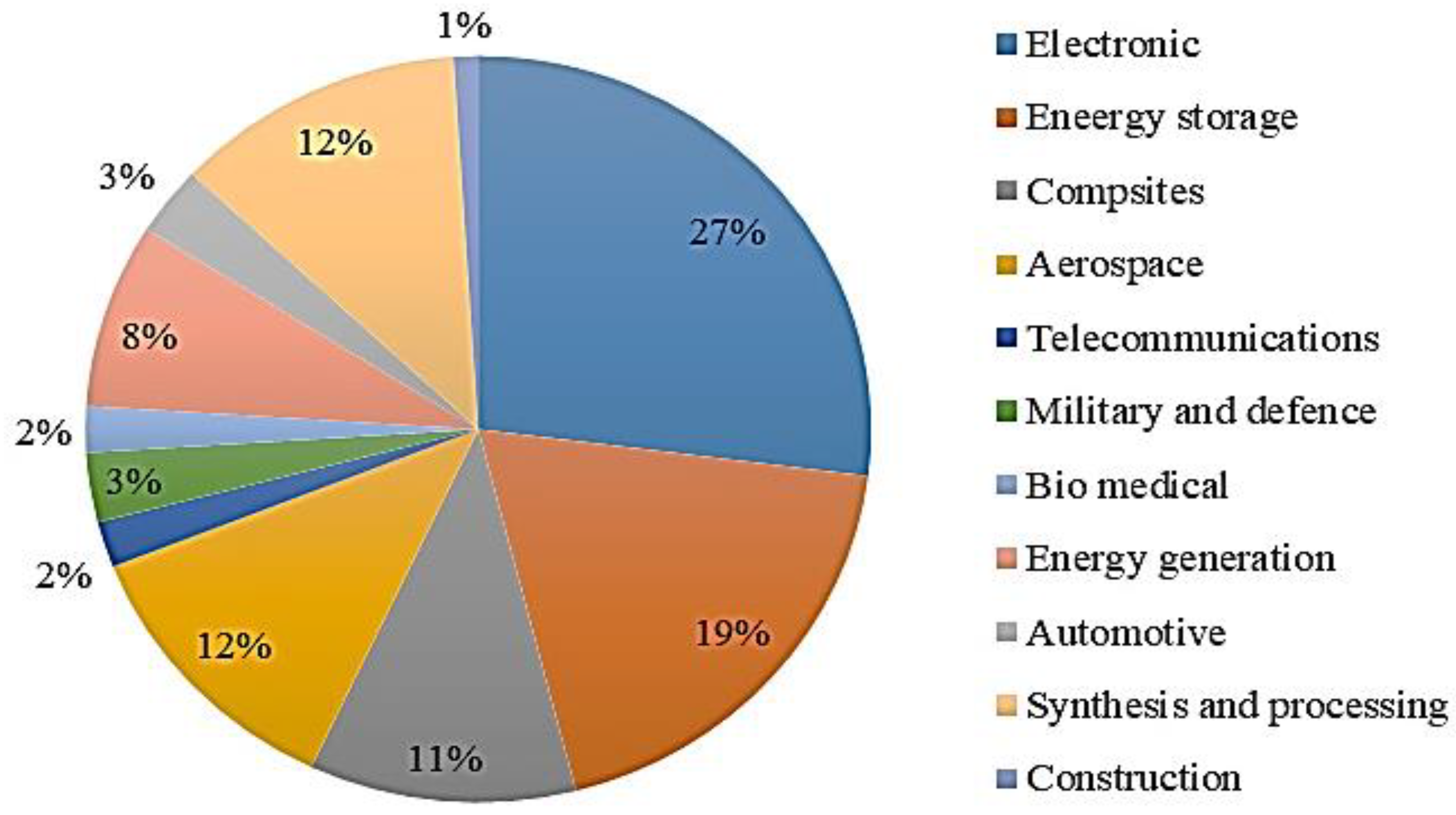
Figure 1. Graphene-based industrial applications are based on the different production sectors.
Sustainability 14 12336 g001
Figure 2. The number of graphene research publications by year, Elsevier, source: Web of Science.
Sustainability 14 12336 g002
Figure 3. (a) Carbon particle atomic structure. (b) The level of energy in carbon atoms from external electrons. (c) The development of sp2 hybrids. (d) In graphene crystal mesh, where A and B are carbon atoms from different substrata, and unit cell vectors are a1 and a2. (e) The sigma bond and the sp2 hybridization µ bond [25].
Sustainability 14 12336 g003
Figure 4. (a) Monolayer graphene honeycomb with white (black) circles indicating carbon-based carbon atoms at sites A(B) and (b) a monolayer lattice with the corresponding Brillouin zone shaded hexane [42].
Sustainability 14 12336 g004
Figure 5. Step-by-step process of graphene production. (a) Micromechanical cleavage. (b) Anodic bonding. (c) Photo exfoliation. (d) Liquid phase exfoliation. (e) Growth on SiC. Gold and grey spheres represent Si and C atoms, respectively. At elevated temperature T, Si atoms evaporate (arrows), leaving a carbon-rich surface that forms graphene sheets. (f) Segregation/precipitation from the carbon-containing metal substrate. (g) Chemical vapour deposition. (h) Molecular beam epitaxy. (i) Chemical synthesis using benzene as a building block [47].
Sustainability 14 12336 g005
Figure 6. The stable graphene production procedures on the scale of 0–3 have vital characteristics. G means graphene quality, s means graphene applicability, p means graphene purity, and y means graphene output [49].
Sustainability 14 12336 g006
Figure 7. Different techniques of graphene synthesis.
Sustainability 14 12336 g007
Figure 8. The graphene’s mechanical exfoliation using Scotch tape from HOPG [58].
Sustainability 14 12336 g008
Figure 9. The chemical extraction process of graphene from graphite [77].
Sustainability 14 12336 g009
Figure 10. Synthetic route of graphene from glucose and dicyandiamide (DCDA) via pyrolysis [93].
Sustainability 14 12336 g010
Figure 11. Schematic representation of fundamental processes during epitaxy [98].
Sustainability 14 12336 g011
Figure 12. (A) Ambipolar electric field effects of monolayer graphene. (B) Changes in resistance of graphene devices concerning gate voltage. (C) Charge carrier density and mobility of graphene as a function of gate voltage. (D) Longitudinal resistance and Hall conductance versus carrier concentration. Illustration of variations in the Hall conductance concerning carrier concentration in bilayer graphene.
Sustainability 14 12336 g012
Figure 14. GNP nanofluids’ thermal conductivity as a function of temperature for different nanoparticle concentrations [128].
Sustainability 14 12336 g014
Figure 15. (a) The spectrum of Raman measuring in a graphic film at several locations, CVD produced in Ni thin films and transferred to SiO2/Si, showing the presence of D, G, and G′ (2D) peaks for single-, bi-, and three-layered regions. (bd) G-band intensity Raman maps of a single graphene layer prepared on Cu foils and transferred in CVD with 12CH4 and 13CH4 to SiO2/Si. During the growth process, 12CH4 and 13CH4 are performed in two steps. (b) The sum of the intensities of the two isotopes’ G bands, (c) the intensity around the 12C G band, and (d) the intensity around 13C G (the two bands are moved by approximately 60 cm−1) [134] © 2009, American Chemical Society (bd).
Sustainability 14 12336 g015
Figure 16. Different types of application of graphene in energy.
Sustainability 14 12336 g016
Figure 17. Applications of graphene particles in medical science.
Sustainability 14 12336 g017
Figure 18. Applications of graphene nanoparticles in the electronics field.
Sustainability 14 12336 g018
Figure 19. (a) Circuit chart of a four-port graphene RF recurrence blender. The extent of the graphene IC is restricted by the ran box. The hexagonal image addresses a graphene FET. The graphene FET here is a long-channel gadget, (b) a preview of the yield range, somewhere in the range of 0 and 10 GHz, of the blender taken from a range analyzer with fRF = 3.8 GHz and fLO = 4 GHz. Every x and y division compares to 1 GHz and 10 dBm, respectively. The graphene FET is one sided at a channel predisposition of 2 V and an entryway voltage of −2 V. The information RF power is acclimated to 0 dBm so the yield range power estimated is the real misfortune (acquire) regarding the RF input. Recurrence blending is apparent with two pinnacles seen at frequencies of 200 MHz and 7.8 GHz with a value force of −27 and −52 dBm, respectively. Figures were copied from [167].
Sustainability 14 12336 g019
Figure 20. SEM images of inkjet-printed composite ink C onto PEL paper: (a) 1 L at 2000×; (b) 1 L at 10,000×; (c) 5 L at 2000×; and (d) 5 L at 10,000×.
Sustainability 14 12336 g020
Figure 21. Applications of graphene nanoparticles in food industries.
Sustainability 14 12336 g021
Figure 22. Applications of graphene nanoparticles in sports.
Sustainability 14 12336 g022
Table 1. Previous research on graphene nanoparticles and their advantages in medical science.
NoReferencesNanocompositesAdvantages
1Li et al. [132]Pt(IV)-conjugated nano-GOTo upgrade the restorative proficiency of Pt drug
2Wang et al. [133]GQDsSynchronous focused on cellular imaging and drug conveyance
3Wang et al. [134]Chlorotoxin-conjugated GOFocused on the conveyance of an anticancer sedate doxorubicin
4Wang et al. [135]GO–gold nanostarsProgressed surface upgraded Raman diffusion detecting and drug conveyance
5Wang et al. [136]RGD-modified chitosan/GO polymersDrug conveyance and biological imaging
6Song et al. [137]Hyaluronic-acid-decorated GO nanohybridsFocused on pH-responsive anticancer drug conveyance
7Ou et al. [138]Fe3O4/SiO2/graphene–CdTe QDs/chitosan nanocompositesTo-the-point drug conveyance
8Liu et al. [139]Polyamide dendrimer and oleic-acid-functionalized grapheneBiocompatible and productive quality conveyance vectors
9Kim and Kim [140]rGO–polyethylenimide nanocompositePhotothermally active DNA delivery
10You et al. [141]Nano-GOCancer detection and medicine delivery
11Rahmanian et al. [142]Nano-GOOral conveyance of flavonoids
12Liu et al. [143]Starch-functionalized graphenepH detective and starch-oriented sedate conveyance
13Yang et al. [144]Go/manganese ferrite nanohybridsMRI, photothermal therapy, and drug conveyance
14Wu et al. [145]Peptide–GO hybrid hydrogelVibrationally triggered drug conveyance
15Tang et al. [146]GO-wrapped mesoporous silica nanoparticles
Table 2. Advantages and uses of graphene nanoparticles in the electronics field.
NoReferencesNanocompositesAdvantages
1Guo et al. [162]G–Pt–PVPHighly sensitive property
2Kempegowda et al. [163]G–PtHighly sensitive in abruptly finding out analyses in compound solution
3Xue et al. [164]G–Au–chitosanHighly sensitive in abruptly finding out analyses in compound solution
4Mondal et al. [165]G–AuHighly sensitive in abruptly finding out analyses in compound solution
5Yin et al. [166]RGO–AuAggressive onset potential and high catalyst stability in fuel cell
6Guo et al. [167]G–PtPdLow CO poisoning in fuel cell
7Mondal and Jana [168]G–noble metalStable catalytic current in fuel cell
8Liang et al. [169]G–CO3O4High catalyst stability in fuel cell
9Zhou et al. [170]G–Si, G–porous SiHighly effective and stable storage capacity in Li-ion batteries
10Wu et al. [171]G–Co3O4Stable and vital performance in continuous cycles in Li-ion batteries
11Zhang et al. [172]G–SnO2Highly effective performance in Li-ion batteries
13Wang et al. [173]G–TiO2High charging and discharging capability and flexibility
Publisher’s Note: MDPI stays neutral with regard to jurisdictional claims in published maps and institutional affiliations.