Article

An Improved Overmodulation Strategy for a Three-Level NPC Inverter Considering Neutral-Point Voltage Balance and Common-Mode Voltage Suppression

1
National Maglev Transportation Engineering R&D Center, Tongji University, Shanghai 201804, China
2
Key Laboratory of Control of Power Transmission and Conversion (SJTU), Ministry of Education, Shanghai 200240, China
3
Key Laboratory of Road and Traffic Engineering of the State Ministry of Education, Shanghai 201804, China
4
College of Transportation Engineering, Tongji University, Shanghai 201804, China
5
School of Electrical Engineering, China University of Mining and Technology, Xuzhou 221008, China
*
Author to whom correspondence should be addressed.
Sustainability 2022, 14(19), 12558; https://doi.org/10.3390/su141912558
Submission received: 3 September 2022 / Revised: 27 September 2022 / Accepted: 29 September 2022 / Published: 2 October 2022
(This article belongs to the Special Issue Sustainability Optimisation of Electrified Railways)

Abstract

:
The three-level neutral-point clamped voltage source inverter (3L-NPC-VSI) is widely used in the maglev traction systems due to its high output voltage, large output capacity and low output current harmonics. In order to improve the utilization of the DC-bus voltage, an overmodulation strategy is necessary. This paper proposes an improved overmodulation strategy based on the minimum amplitude error method for a 3L-NPC-VSI. Compared with the conventional overmodulation strategy based on the minimum amplitude error method, the utilization of the DC-bus voltage is higher. Meanwhile, a virtual space vector modulation strategy is adopted for inverter neutral-point (NP) voltage balance and common-mode voltage (CMV) suppression. Furthermore, the suppression of leakage current also has been verified. Furthermore, the implementation details of the proposed overmodulation strategy based on minimum amplitude error method is elaborated. The effectiveness of the proposed method is verified by simulation and experimental results.

1. Introduction

The three-level neutral-point clamped voltage source inverter (3L-NPC-VSI) is widely used, not only in the industrial drives systems, but also transportation fields. It is preferred in many high-power scenarios, such as high-speed maglev traffic linear motor drive system [1,2,3]. This is due to its advantages such as simple topology, lower ripple and total harmonic distortion of output voltage and current compared to the two-level VSI [4,5,6].
Typically, an inverter can operate in the overmodulation region to fully exploit the DC-bus voltage, which can provide significant voltage improvement in many applications [7,8]. This is crucial for improving the output performance of the inverters, especially in the motor drive systems [9]. Therefore, the overmodulation strategy should be adopted to improve the inverter output performance. Furthermore, the effective usage of the overmodulation algorithm still guarantee the original performance when the DC-bus voltage drops. Commonly, overmodulation strategies is divided into two types, one is single-mode overmodulation strategy, the other is dual-mode overmodulation strategy. Except for the minimum angle error algorithm, some other single-mode overmodulation strategies, such as the minimum amplitude error method and the minimum vector error method, were proposed to increase the amplitude of output voltage vectors. The voltage projection of the minimum amplitude error algorithm is perpendicular to the hexagon boundary, while the voltage projection of the minimum vector error algorithm is parallel to the relative voltage vector with higher modulation index (MI) [9,10,11]. If the reference voltage vector is high enough, six-step operation will be achieved after voltage correction using these two improved algorithms, i.e., the output voltage vectors are the basic voltage vectors [12].
Considering classical dual-mode overmodulation strategy in [13], only the amplitude of reference voltage vector is modified based on the minimum angle error method in the first part of the overmodulation region. The amplitude and the angle of the reference voltage vector are both modified in the second part of the overmodulation region. A modified dual-mode algorithm has been presented in [14,15] to obtain the better harmonic performance. However, the dual-mode overmodulation strategy generally requires significant computational effort due to different variables and calculation procedures [16]. In [17], a novel overmodulation strategy based on voltage vector space division has been proposed to solve the problem that the voltage jumps between output voltage vectors in high overmodulation regions cause the deterioration of current performance and loading capability.
The algorithm complexity of single-mode overmodulation strategy is lower than that of the dual-mode overmodulation algorithm. In [18], the correction of the voltage vector is realized based on the minimum amplitude error method. Two implementation approaches, modulated model predictive control and space vector pulse width modulation (SVPWM), was provided to verify the overmodulation strategy on a two-level VSI with RL load. However, when the reference voltage vector operates in the overmodulation region in steady state, the method in [18] does not compensate for the output voltage defect caused by the overmodulation. Thus, its DC-bus voltage utilization is lower than that of the dual-mode overmodulation strategy. In general, the algorithm complexity of the single-mode overmodulation algorithm based on the minimum amplitude error method is almost the same as that of the dual-mode strategy, because the amplitude and angle usually need to be corrected [17].
The balance of the neutral-point (NP) voltage is important for the 3L-NPC-VSI, which is the premise of operation. The unbalancing of the NP voltage will increase harmonics, reduce output power quality and damage switching devices in power systems [19,20,21]. Shaft voltage and bearing current will be generated by the common-mode voltage (CMV), which may destroy the motor insulation in motor drive applications and increase the leakage current in the distributed generation applications [22,23,24,25]. Virtual space vector PWM (VSVPWM) provides a new idea for the NP voltage control and the CMV suppression [26,27,28,29,30,31,32,33]. A novel VSVPWM considering NP voltage balance and CMV suppression is proposed in [23]. In [26], a control strategy to realize the asymmetric control of the DC-bus voltages with VSVPWM is studied. In [29], a switched-capacitor multilevel inverter with voltage boosting and CMV reduction capabilities has been studied. In [31], a novel modulation method has been proposed to reduce the CMV and balance the NP voltage and apply to the line voltage coordinate system.
The main contributions of this work are summarized as follows:
  • An overmodulation strategy based on minimum amplitude error method is proposed to improve the utilization of DC-bus voltage;
  • A VSVPWM strategy is adopted to balance the NP voltage and suppress the CMV, and the leakage current has also been effectively suppressed;
  • The difficulty of obtaining key variables in the overmodulation strategy is simplified by fitting.
The rest of paper is organized as follows. Section 2 presents the basic model of the 3L-NPC-VSI system. The principle of the proposed method is given in Section 3. Section 4 presents the VSVPWM strategy considering the NP voltage balance and CMV suppression. Simulation and experimental results are shown and analyzed in Section 5. Finally, the conclusions are drawn in Section 6.

2. Model of 3L-NPC-VSI

For a 3L-NPC-VSI, the MI of the reference voltage vector can be expressed as:
M I = | u r e f | 2 V d c / 3
where uref represents the amplitude of the reference voltage vector, and Vdc is the DC-bus voltage.
Figure 1 shows the topology of a 3L-NPC-VSI and its load. The 3L-NPC-VSI has 27 different switch states that together with the dc voltage can generate 19 voltage space vectors, as presented in the following:
u s = V d c 6 2 1 2 j 3 2 1 2 + j 3 2 1 1 + j 3 1 2 + j 3 2 1 1 2 j 3 2 1 j 3 S
where us are the voltage vectors; S = [ S a   S b   S c ] T is the switching state vector of the inverter, and S x 2 , 1 , 0 is the switching state of phase x a , b , c . Take A-phase as an example, Sx = 2 means that switch Sa1 and Sa2 are closed, Sx = 1 means that switch Sa2 and Sa3 are closed, while Sx = 0 means that switch Sa3 and Sa4 are closed.

3. Proposed Overmodulation Strategy

This section proposes an improved dual-mode overmodulation strategy based on the minimum amplitude error method.
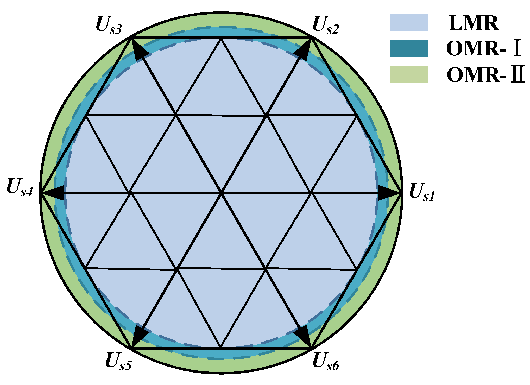
According to Figure 2, the space voltage vector diagram is divided into linear modulation region (LMR), overmodulation region I (OMR-I) and overmodulation region II (OMR-II). The LMR is the inscribed circle of the large regular hexagon of the inverter, and the maximum MI in the LMR is 0.866. The maximum MI in the OMR-I is determined by the voltage-area equivalence. The amplitude of the voltage vector within the boundary of the hexagon will increase to compensate for voltage loss caused by overmodulation. The final result is that, in one electrical cycle, the area of the ideal reference voltage vector circle is equal to the area enclosed by the corrected voltage vector. Therefore, the maximum MI satisfying the voltage-area equivalence principle is 0.909. The maximum MI in the OMR-II is 0.955, which is limited by the fundamental voltage output capability of the inverter.
As shown in Figure 2, the LMR, the OMR-I and the OMR-II corresponds to the MI range [0,0.866], [0.866,0.909] and [0.909,0.955], respectively.

3.1. LMR

According to the MI of reference voltage vector, the region where the reference voltage vector is located in is determined. When the reference voltage vector uref is located in the LMR, the synthesis of voltage vector is based on the nearest three vectors principle.

3.2. OMR-I

In this work, when the reference voltage vector is located in the OMR-I (0.866 ≤ MI ≤ 0.909), the voltage defect caused by the overmodulation is compensated by increasing the voltage amplitude. As shown in Figure 3a, the orange arc S1 represents the theoretical reference voltage trajectory, the defect voltage generated by overmodulation causes that the fundamental voltage of the inverter cannot reach the reference voltage amplitude. The defect voltage is compensated by increasing the reference voltage vector circle to S2 according to the area equivalent principle. The blue curve in Figure 3a is the actual reference voltage vector trajectory, which will not cause any voltage loss. The u*ref in Figure 3 represents the modified voltage vector.
The mathematical relationship between the MI and the M I * of S2 can be expressed as:
M I 2 = 3 12 M I * 2 - 9 + 12 M I * 2 γ 2 π
However, Formula (3) is a transcendental equation and cannot be solved directly. In this work, piecewise linear fitting is performed on the functional relationship between the MI and the M I * , and the expression of M I * is obtained as follows:
M I * = 29.855 × M I 2 50.9 × M I + 23 ,   0.866 < M I 0.897 126.5 × M I 2 224.233 × M I + 100.3 ,   0.897 < M I 0.905 1029 × M I 2 1859 × M I + 841 ,   0.905 < M I 0.909
The OMR-I is divided into compensation region and equivalent region according to the angle θ in this article. As shown in Figure 3a, S2 intersects the hexagon boundary at point d, and |ed| intersects S1 at point f, | e d | | d h | . |ed| is the boundary between the equivalent region and the compensation region. It should be noted that αr varies with the MI. When the MI changes, the αr needs to be recalculated to prevent the utilization of DC-bus voltage from dropping. The αr can be expressed as:
α r = π 6 - arcsin ( | o e | 2 M I )
Where,
| o e | = 4 M I * 2 3
The reference voltage vector u r e f will locate in the compensation region if the angle θ satisfies 0 θ α r or π / 3 α r θ π / 3 , otherwise in the equivalent region.

3.2.1. Vector Correction of Equivalent Region

In this work, when the reference voltage vector uref is located in the equivalent region, the correct rule of uref based on minimum amplitude error method. As shown in Figure 3b, the correction rules do not change whether the reference vector uref falls inside the hexagon boundary.
If the reference voltage vector uref is located outside of hexagon, as shown in Figure 3b, the VSI works in the overmodulation zone. In this case, the VSI is not able to synthesize the reference vector without distortions by using the basic voltage vectors. However, it is still possible to synthesize another reachable voltage vector that has the least distance from the reference vector for a minimum tracking error based on minimum amplitude error method.
According to Figure 3b, it is easy to obtain:
| a b | = | - 3 M I cos ( θ ) M I sin ( θ ) + 3 | 2
| a c | = ( M I cos ( θ ) 1 ) 2 + ( M I sin ( θ ) ) 2
| b c | = | a b | 2 + | a c | 2
where θ is the angle of reference voltage vector, as shown in Figure 3b.
The MI* of the modified voltage vector u r e f can be solved according to the trigonometric function relationship and the Pythagorean theorem accurately. The MI* can be expressed as:
M I * = | b c | 2 | b c | + 1
Similarly, the corrected reference voltage vector angle θ * can be solved by the triangular relationship and be expressed as:
θ * = arctan ( 3 | b c | 2 | b c | )

3.2.2. Vector Correction of Compensation Region

As shown in Figure 3c, if the reference voltage vector is located in the grey region, i.e., 0 θ α r or π / 3 α r θ π / 3 , it will be the compensation region. In this work, the calculation of MI* is based on Equation (5) to compensate for the voltage loss caused by overmodulation. In the OMR-I, in order to realize the smooth transition of the vector trajectory between the equivalent region and the compensation region, the vector angle θ needs to be corrected.
According to Figure 3c, the blue curve represents the actual voltage vector trajectory. | e d | is the boundary between the equivalent region and the compensation region, and | e d | | d h | . The location of point e can be determined by the MI and calculated by Equation (6). The uref represents the reference voltage vector. | e g | is extended and it intersect with the actual reference voltage trajectory at v. The calculation process of the new angle θ * of the u r e f * is as follows.
According to Figure 3, it is easy to obtain:
| e g | = M I 2 + | o e | 2 2 M I | o e | cos ( θ )
| e v | = | e g | R
where R represents the similarity ratio between △egs and △evt.
The R can be expressed as:
R = M I | o e | M I * | o e |
In Δoev, the new angle θ * can be expressed as:
θ * = arccos ( M I * + | o e | 2 | o g | 2 2 M I * | o e | )
Substituting Equations (6), (12), (13) and (14) into Equation (15), the new angle θ * of the reference voltage vector in the compensation region can be obtained.
It is worth noting that the corrected result of reference voltage vector in the common boundary are consistent, so the transition of the reference voltage vector between the two regions is smooth and continuous.

3.3. OMR-II

When the MI exceeds 0.909, the reference voltage vector is located in the OMR-II, the voltage defect caused by the overmodulation cannot be compensated completely similar to OMR-I. Therefore, in order to maximize the utilization of DC-bus voltage, the proposed method divides OMR-II into equivalent region and holding region.
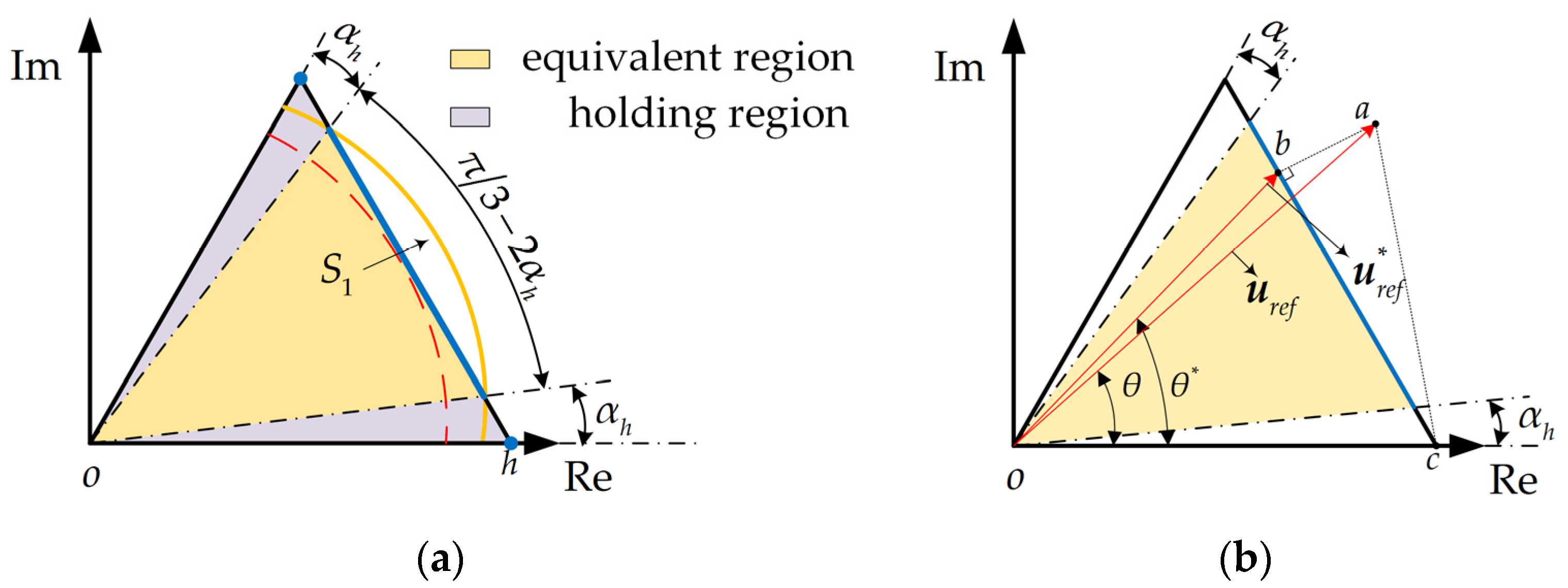
As shown in Figure 4a, take the first sector as an example, the division of the equivalent region and the holding region is based on the holding angle αh. In order to simplify the calculation of αh, this paper obtains αh by the method of piecewise linear fitting. The αh can be expressed as:
α h = 6.702 × M I 6.09 ,   0.909 < M I 0.936 12.305 × M I 11.34 ,   0.936 < M I 0.953 51.27 × M I 48.43 ,   0.953 < M I < 0.955
In OMR-II, if the θ satisfies 0 θ α h or π / 3 α h θ π / 3 , the reference voltage vector will locate in the holding region, otherwise in the equivalent region.

3.3.1. Vector Correction of Equivalent Region

As shown in Figure 4, the correction rule of the reference voltage vector located in the equivalent region of the OMR-II does not change compared with that in the OMR-I. The new modulation index MI* of corrected reference voltage vector can be calculated by Equation (10) and the new angle θ * of corrected reference voltage vector can be calculated by Equation (11).

3.3.2. Vector Correction of Holding Region

In order to ensure the maximum utilization of the DC-bus voltage, the nearest large basic voltage vector will be kept output when the reference voltage vector is located in the holding region, as shown in Figure 4a.
In this paper, the working region of the inverter is judged according to the magnitude of MI as shown in Figure 3 and Figure 4. It is worth noting that in the overmodulation strategy proposed in this paper, the MI is calculated by the reference voltage according to Equation (1), and θ depends on estimation or measurement.

4. NP Voltage Balance and CMV Suppression

In this section, a virtual space vector method considering NP voltage balance and CMV suppression is introduced. The small virtual vector and medium virtual vector can be constructed by three adjacent basic vectors [22].
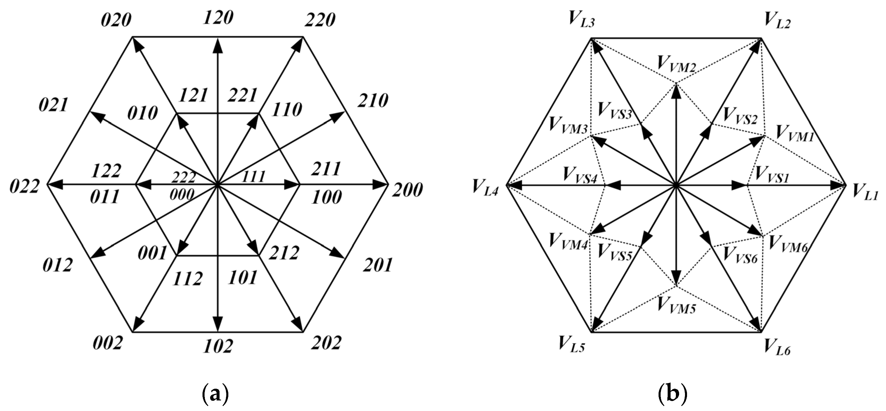
As shown in Figure 5a, the 3L-NPC-VSI has a total of 27 basic switching states vectors. When synthesizing virtual vectors, the basic voltage vectors which generate a CMV exceeding Vdc/6 are not used [27]. Therefore, the small virtual vector VVS1 and VVS2 constructed by three adjacent small basic vectors with a low CMV (CMV ≤ Vdc/6) can be expressed as:
V V S 1 = 1 3 V ( 101 ) + 1 3 V ( 211 ) + 1 3 V ( 110 )
V V S 2 = 1 3 V ( 211 ) + 1 3 V ( 110 ) + 1 3 V ( 121 )
The medium virtual vector VVM1 constructed by three adjacent basic vectors with a low CMV can be expressed as:
V V M 1 = 1 3 V ( 120 ) + 1 3 V ( 210 ) + 1 3 V ( 201 )
The average value of the NP current of VVS1, VVS2 and VVM1 in one switching cycle can be expressed as:
i V S 1 = 1 3 ( i b i c i a ) = 0
i V S 2 = 1 3 ( i a i c i b ) = 0
i V S 1 = 1 3 ( i a + i b + i c ) = 0
where ia, ib and ic represent the NP current produced by the fundamental voltage vector participating in the synthesis of virtual vector [23].
According to Equations (20)–(22), the constructed virtual vectors with zero NP current does not affect the NP voltage. Figure 5b shows the division of the virtual space vector diagram considering NP voltage balance and CMV suppression.

5. Simulation and Experimental Results

The effectiveness of the proposed method has been validated using the simulation studies in the MATLAB/Simulink. The experimental test bench of the 3L-NPC-VSI with RL load is built to verify the proposed method. The parameters of 3L-NPC-VSI with RL load are listed in Table 1.

5.1. Simulation Results

5.1.1. NP Voltage Balance and CMV Suppression

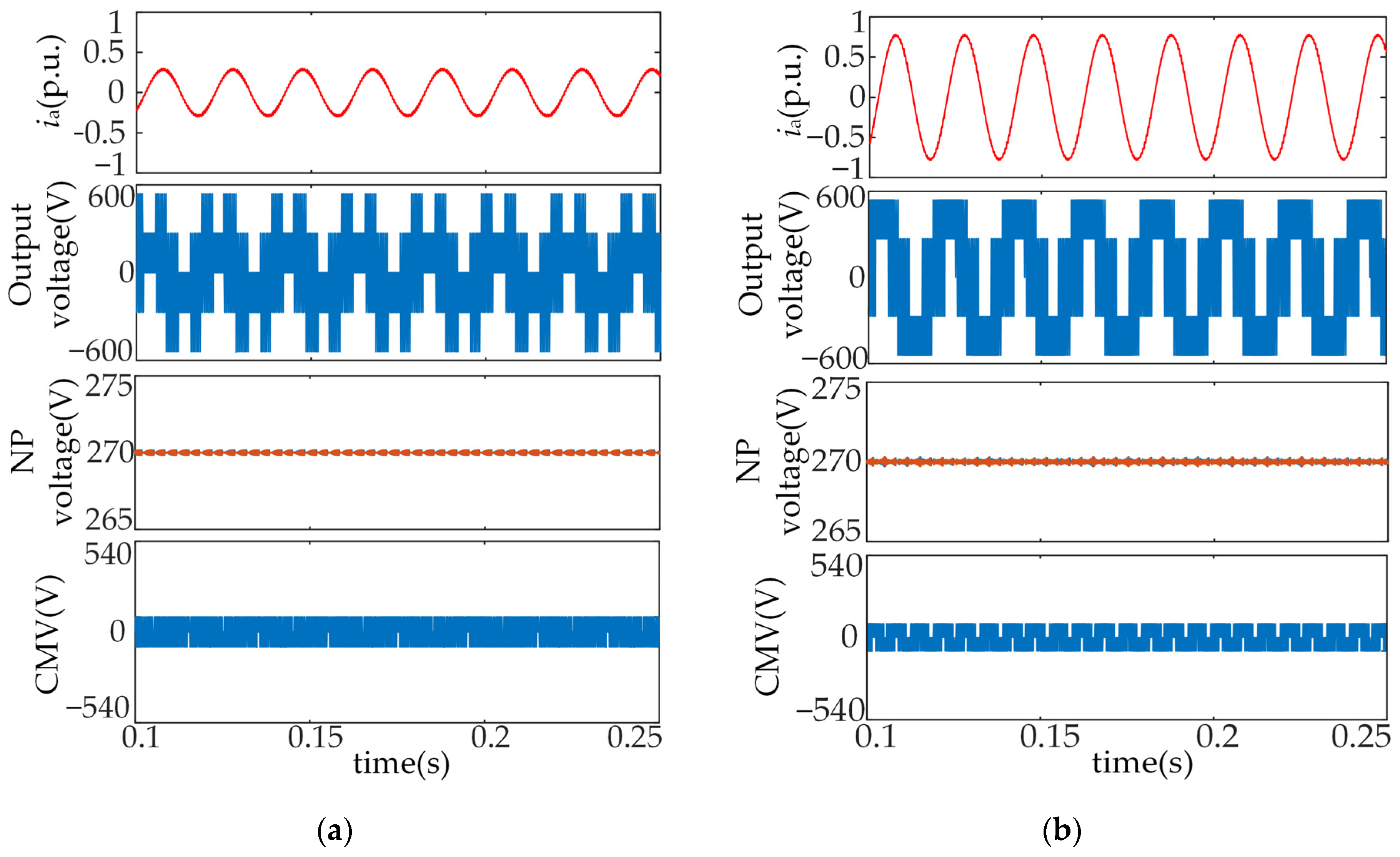
Figure 6 shows the simulation results of proposed strategy in the LMR (0 < MI < 0.866). Figure 6 shows the simulation results when the MI is equal to 0.3 and 0.8, respectively. From top to bottom are the a-phase current ia (p.u.), output voltage, NP voltage and CMV.
According to Figure 6, when the reference voltage vector is located in the LMR, the CMV of the 3L-NPC-VSI with RL load is suppressed effectively, and its peak-to-peak value is equal to 180 V. At the same time, the voltage of the upper and lower capacitors on the DC-bus also achieves excellent balance effect.
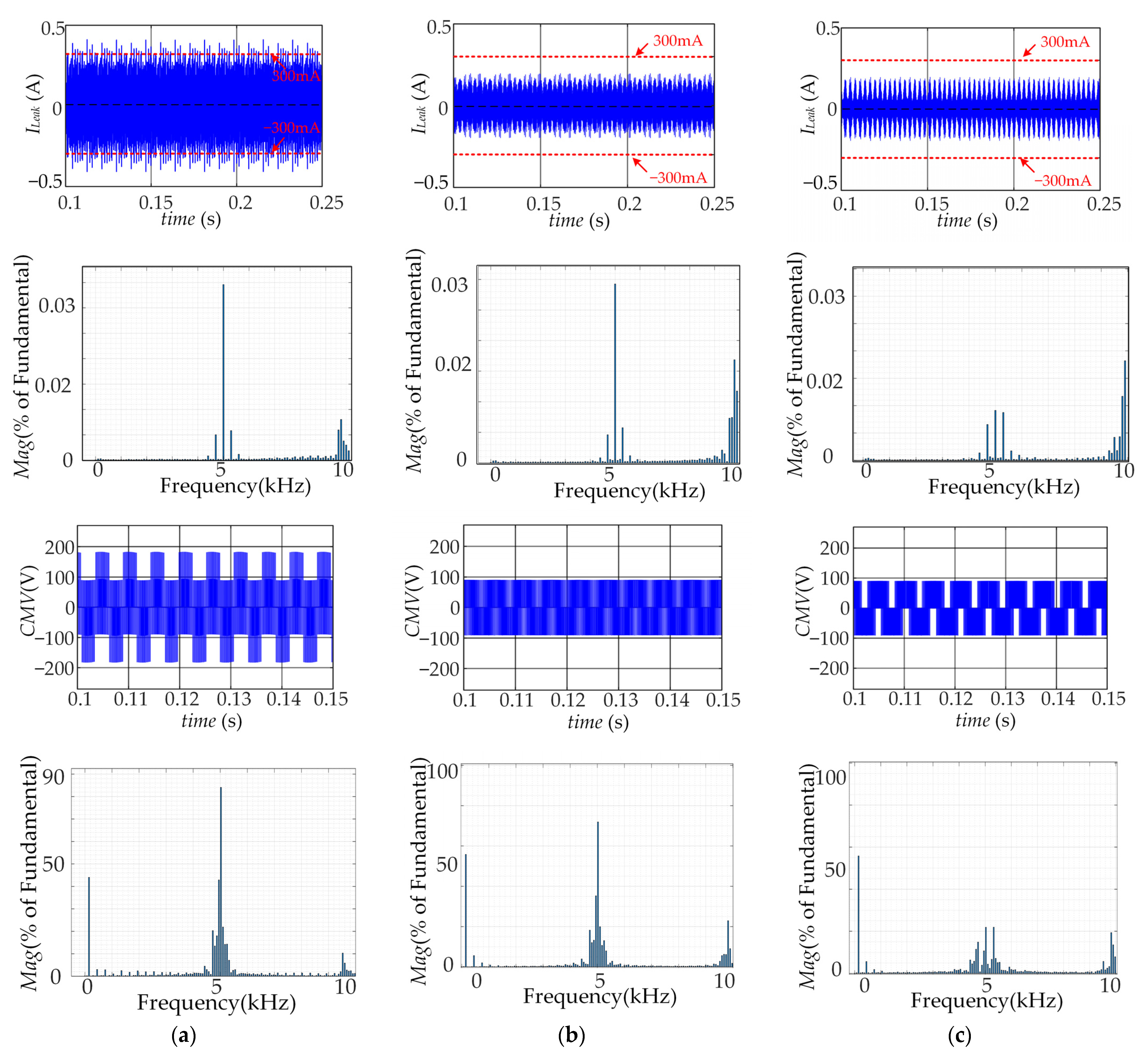
The simulation results of leakage current and CMV when the MI is equal to 0.8 are shown in Figure 7, from top to bottom are the leakage current waveform, the Fast Fourier Transformation (FFT) result of the leakage current, the CMV waveform and the FFT result of the CMV. The traditional SVPWM method and VSVPWM method considering common-mode voltage rejection in [28] are adopted for comparison. As shown in Figure 7a, when the SVPWM method is adopted, the magnitude of the leakage current reaches 400 mA, which fails to comply with the standard level of 300 mA [29]. When the other two methods are adopted, the magnitude of the leakage current is limited effectively within the 300 mA. According to the FFT results of leakage current as shown in Figure 7, the high-frequency components around 5 kHz are slightly reduced compared with the SVPWM method when the VSVPWM method in [28] is adopted. When the VSVPWM method in this paper is adopted, the high-frequency components around 5 kHz are reduced greatly compared with those of the other two methods. This also means that power losses are significantly reduced [33]. Therefore, the power losses can be inferred based on the high-frequency components according to the simulation results. The comparison of different methods is listed in Table 2.
According to the waveforms of the CMV and FFT results of the CMV in Figure 7, both VSVPWM methods achieve CMV suppression effectively. However, the high-frequency components around 5 kHz and 10 kHz are obviously decreased when the VSVPWM method in this paper is adopted. As shown in Figure 7, the FFT results of leakage current and the FFT results of CMV show consistency when the three methods are adopted. In addition, the high-frequency components around 5 kHz in the leakage current spectrum and CMV spectrum are lower than those of the other methods obviously when the VSVPWM method in this paper is adopted.

5.1.2. Improvement of DC-Bus Voltage Utilization

The overmodulation strategy mentioned in [18] is a classic overmodulation strategy based on the minimum amplitude error method, which is called the conventional overmodulation strategy in this article. Its defect is that the utilization of DC-bus voltage will be decreased when the reference voltage vector is located in the OMR-I. The overmodulation strategy proposed in this paper improves this deficiency.
A new correction method for the reference voltage vector located in the OMR-I is proposed. It is worth noting that when the MI exceeds 0.909, there is no difference in the correction rule between conventional overmodulation strategy and proposed strategy.
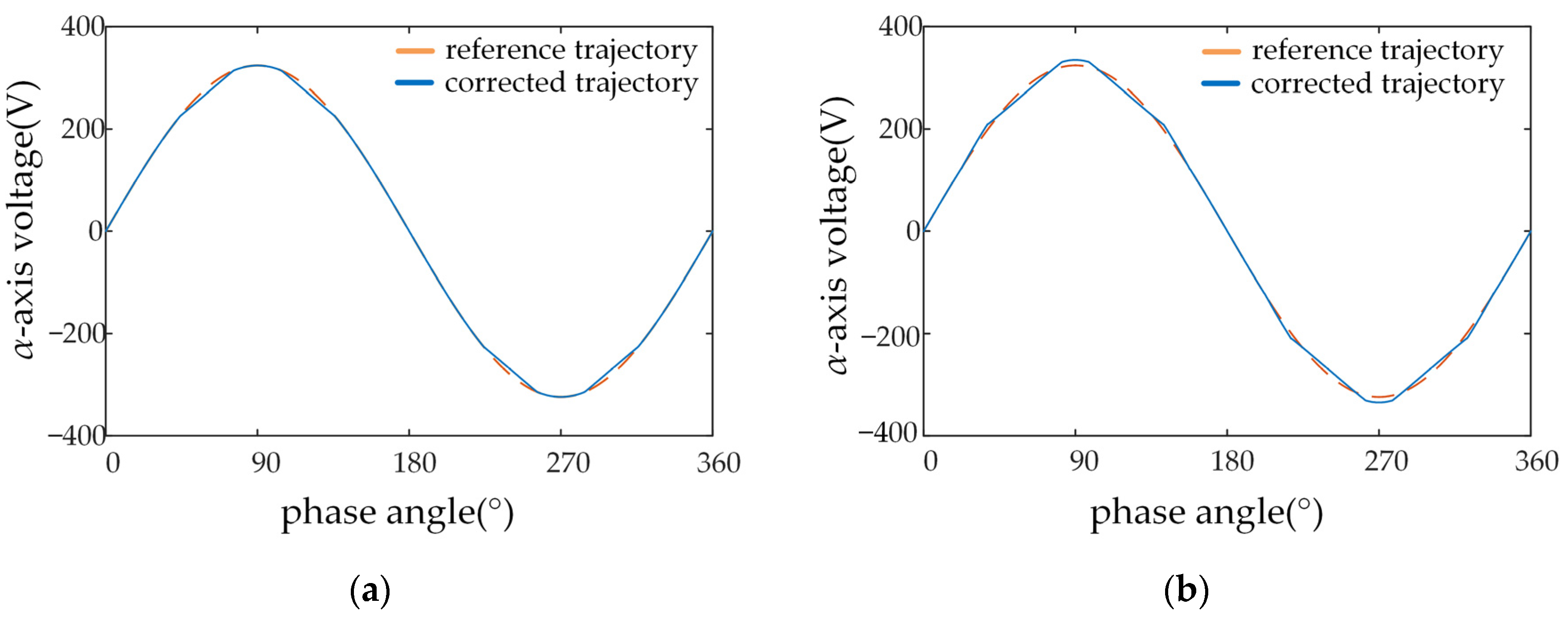
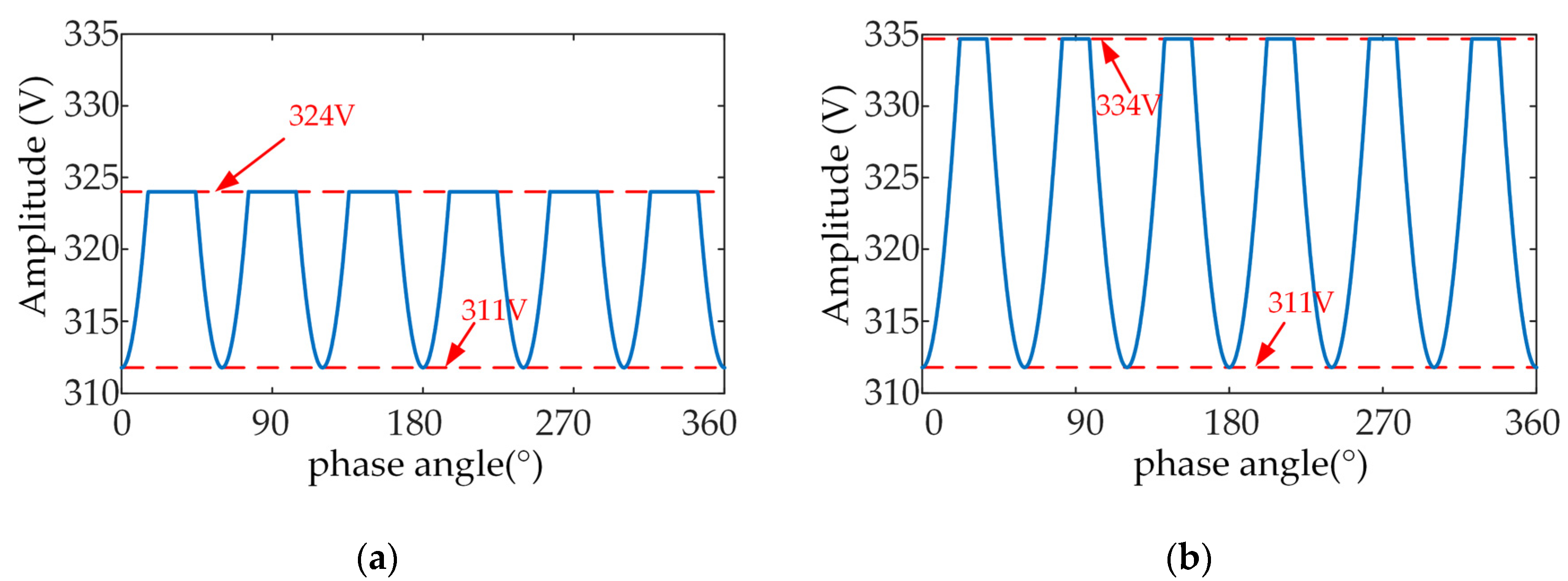
Figure 8 shows the α-axis voltage correction waveforms in an electrical cycle of the conventional overmodulation method and the proposed strategy in this paper when the MI is equal to 0.9. Figure 9 shows the magnitude of the reference voltage vector after correction in an electrical cycle. It can be seen that the curve part is the amplitude of equivalent voltage vector based on the minimum amplitude error method. Meanwhile, the voltage vector operates on the hexagonal boundary, and the minimum voltage vector amplitude is 311 V. According to Figure 9, the maximum amplitude of corrected voltage vector is 324 V when the conventional overmodulation strategy is adopted. However, when the proposed strategy is adopted, the maximum amplitude of corrected voltage vector is 334 V. It can be seen that the higher utilization of DC-bus voltage has achieved when the proposed method is adopted.
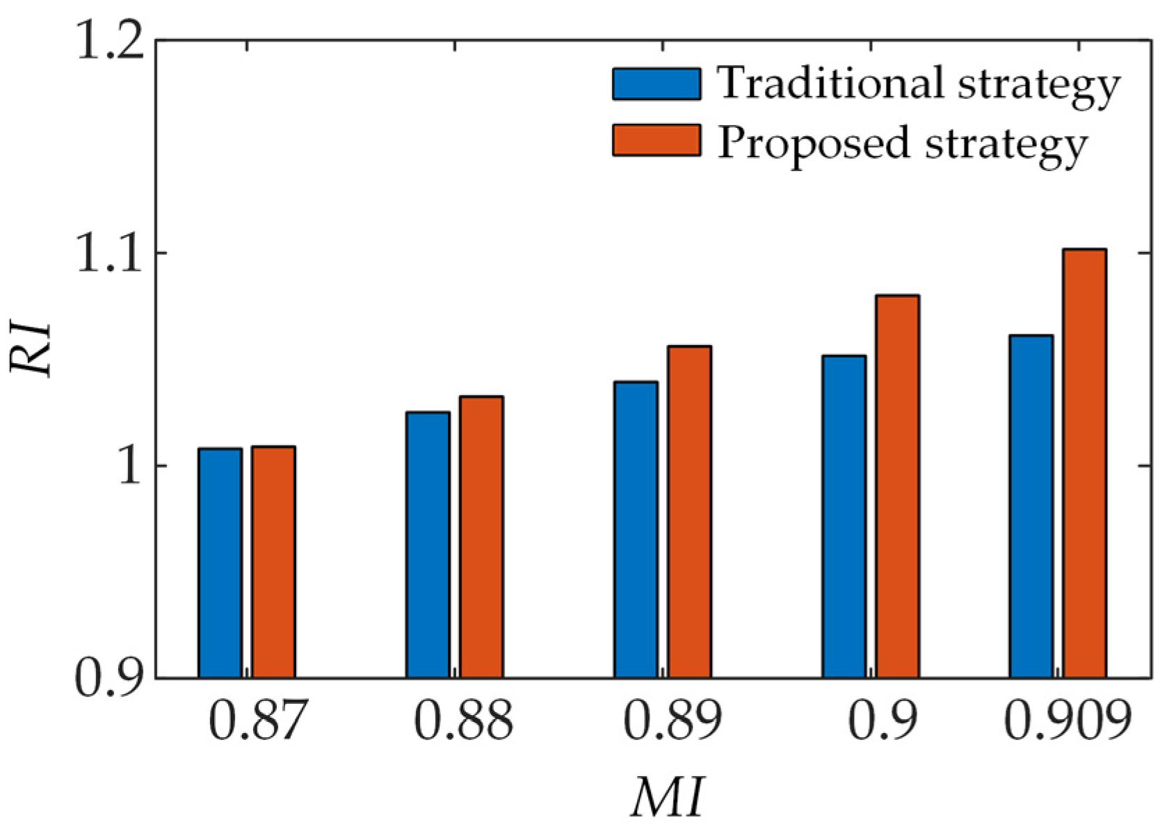
Figure 10 shows the comparison of RI by the conventional strategy versus the proposed strategy when MI increases from 0.866 to 0.909. The RI can be expressed as:
R I = S c o r r e c t e d S f u n d a m e n t a l
where Scorrected is the area of the region enclosed by the corrected voltage vector trajectory in one electrical cycle; Sfundamental is the area enclosed by the voltage vector trajectory when the MI is equal to 0.866.
According to Figure 10, the RI increases with the MI. When the MI is equal to 0.909, the RI of the proposed strategy is 1.1, which increases by 3.77% compared with the conventional strategy. Notably, this illustrates the improved utilization of the DC-bus voltage.

5.2. Experimental Results

The effectiveness of the proposed overmodulation strategy based on minimum amplitude error and considering NP voltage balance and CMV suppression is verified on a 3L-NPC-VSI platform. The DC-bus voltage is set to 540 V. The proposed overmodulation algorithm is implemented on a TMS320F28335 DSP. The PWM frequency is set to 5 kHz.
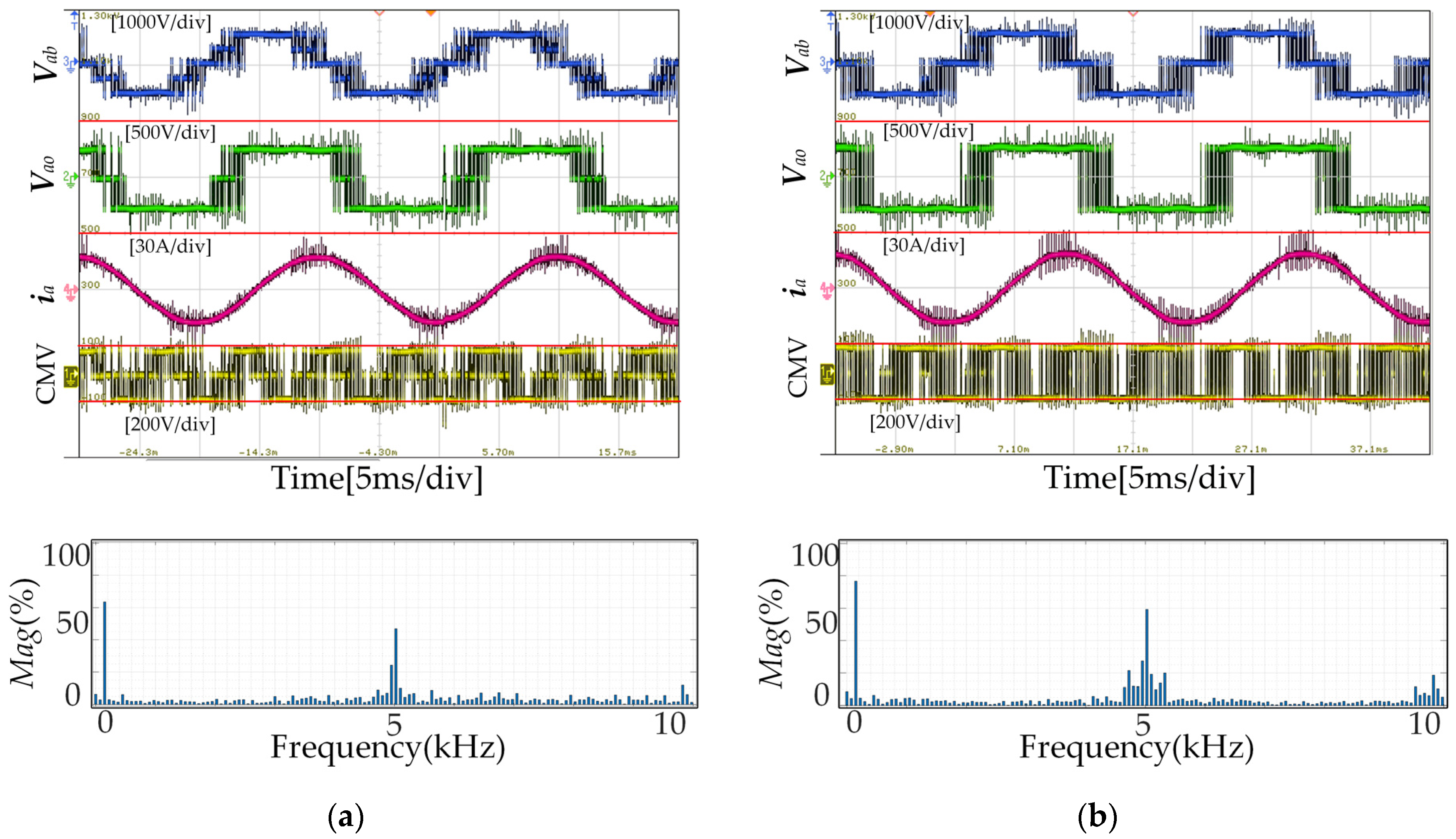
Figure 11 presents the experimental results of the proposed method in the LMR, from top to bottom are the voltage Vab, voltage Vao, output a-phase current ia, CMV and CMV spectrum. Figure 11a,b show the experimental results when the MI is equal to 0.3 and 0.8, respectively. Figure 12 presents the experimental results of the proposed method in the OMR-I and OMR-II, from top to bottom are voltage Vab, voltage Vao, output a-phase current ia, CMV and CMV spectrum. Figure 12a,b show the experimental waveforms when the reference voltage vector is located in the OMR-I (MI = 0.9) and OMR-II (MI = 0.95), respectively. The amplitude of CMV is suppressed effectively when the proposed method is adopted, as shown in Figure 11 and Figure 12. According to the CMV spectrum shown in Figure 11 and Figure 12, as the MI increases, the high-frequency components of CMV increases. Compared with the results shown in Figure 7c, the FFT results of CMV are same basically. According to Figure 11 and Figure 12, the experimental results verify the effect of the method in this paper on the suppression of the CMV, the reduction of leakage current and the validity of the proposed overmodulation strategy.
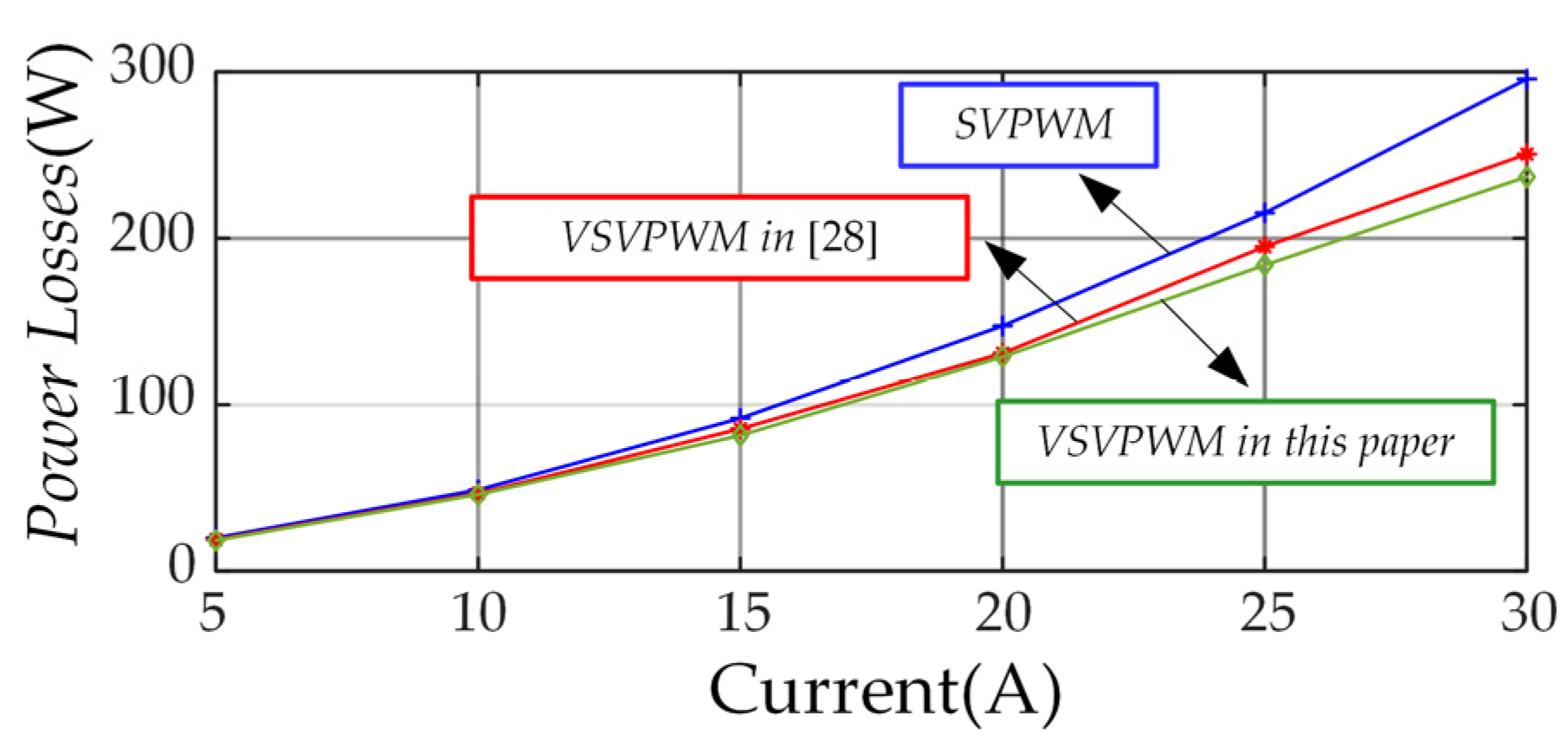
Figure 13 shows the power losses of the 3L-NPC-VSI with the SVPWM, VSVPWM in [28] and VSVPWM in this paper, where the output current varies from 5 to 30 A. The power losses for the VSVPWM method in this paper is 237 W while it is 250.6 W for the VSVPWM method in [28] and 295.7 W for the SVPWM method when the output current is increased to 30 A. Therefore, the power loss of the proposed method is 5.7% less than that of the conventional VSVPWM and 24.8% less than that of the SVPWM.
Figure 14 shows the efficiency comparison among the SVPWM, VSVPWM in [28] and VSVPWM in this paper under different output current, in which the input power is calculated by multiply DC-bus voltage with current. Then efficiency is calculated by the ratio of input power and output power. When output current ranges from 5 to 30 A, the SVPWM has the lowest efficiency due to high leakage current. The VSVPWM method in this article has the highest efficiency, which is followed by conventional VSVPWM method. This is because the high-frequency components around 5 kHz are greatly reduced compared with those of the other two methods when the VSVPWM method in this paper is adopted.

6. Conclusions

This paper discusses the implementation details of the proposed overmodulation strategy considering the NP voltage balance and CMV suppression. In order to improve the utilization of DC-bus voltage, an improved overmodulation strategy based on the minimum amplitude error method for a 3L-NPC-VSI is proposed. Compared with the conventional overmodulation strategy based on the minimum amplitude error method, the utilization of the DC-bus voltage is increased. The VSVPWM method is adopted for the balance of NP voltage and the suppression of CMV. The leakage current is also limited effectively within the standard value according to the simulation results. Eventually, experimental and simulation results verify the effectiveness of the proposed method.

Author Contributions

Project administration, Z.M.; software, H.N. and X.W.; supervision, G.L.; validation, X.W. and X.Z.; writing—original draft, H.N.; writing—review and editing, Z.M. All authors have read and agreed to the published version of the manuscript.

Funding

This research was supported by Key Laboratory of Control of Power Transmission and Conversion (SJTU), Ministry of Education (2021AC05) and by Natural Science Foundation of Shanghai (No. 20ZR1461100).

Data Availability Statement

Not applicable.

Conflicts of Interest

The authors declare no conflict of interest.

References

  1. Zhang, B.; Yang, P.; Ge, Q.; Wang, X.; Li, Y. A New High Output Frequency Multilevel Inverter Topology of Traction Converter for Superspeed Maglev Train. In Proceedings of the 2021 13th International Symposium on Linear Drives for Industry Applications (LDIA), Wuhan, China, 1–3 July 2021; pp. 1–5. [Google Scholar]
  2. Lee, J.; Jo, J.; Han, Y.; Lee, C. Development of LSM Control System for Super Speed Maglev. In Proceedings of the 2013 13th International Conference on Control, Automation and Systems (ICCAS 2013), Gwangju, Korea, 20–23 October 2013; pp. 466–469. [Google Scholar]
  3. Ma, Z.; Sun, Y.; Zhao, Y.; Zhang, Z.; Lin, G. Dichotomy Solution Based Model Predictive Control for Permanent Magnet Linear Synchronous Motors. In Proceedings of the 2019 22nd International Conference on Electrical Machines and Systems (ICEMS), Harbin, China, 11–14 August 2019; pp. 1–5. [Google Scholar]
  4. Nabae, A.; Takahashi, I.; Akagi, H. A New Neutral-Point-Clamped PWM Inverter. IEEE Trans. Ind. Appl. 1981, IA-17, 518–523. [Google Scholar]
  5. Teichmann, R.; Bernet, S. A comparison of three-level converters versus two-level converters for low-voltage drives, traction, and utility applications. IEEE Trans. Ind. Appl. 2005, 41, 855–865. [Google Scholar]
  6. Jiang, H.; Deng, F.; Wang, Z.; Zou, Z.; Li, B.; Blaabjerg, F. Harmonic Optimization Strategy for CPS-PWM Based MMCs Under Submodule Capacitor Voltage Reduction Control. IEEE Trans. Power Electron. 2022, 37, 4288–4300. [Google Scholar]
  7. Kwon, Y.; Kim, S.; Sul, S. Six-step operation of PMSM with instantaneous current control. IEEE Trans. Ind. Electron. 2014, 50, 2614–2625. [Google Scholar]
  8. Stumpf, P.; Halàsz, S. Optimization of PWM for the overmodulation region of two-level inverters. IEEE Trans. Ind. Appl. 2018, 54, 3393–3404. [Google Scholar]
  9. Nasiri, M.; Mobayen, S.; Arzani, A. PID-type Terminal Sliding Mode Control for Permanent Magnet Synchronous Generator-based Enhanced Wind Energy Conversion Systems. CSEE J. Power Energy Syst. 2022, 8, 993–1003. [Google Scholar]
  10. Pujol-Vazquez, G.; Acho, L.; Mobayen, S.; Nápoles, A.; Pérez, V. Rotary inverted pendulum with magnetically external perturbations as a source of the pendulum’s base navigation commands. J. Frankl. Inst. 2018, 355, 4077–4096. [Google Scholar]
  11. Alsofyani, I.M.; Lee, K. Improved transient-based overmodulation method for increased torque capability of direct torque control with constant torque-switching regulator of induction machines. IEEE Trans. Power Electron. 2020, 35, 3928–3938. [Google Scholar]
  12. Yun, J.; Son, Y.-K.; Sul, S.-K. Parallel Operation of Permanent Magnet Synchronous Generators under Six-Step Operation Mode. In Proceedings of the 2022 IEEE Transportation Electrification Conference & Expo (ITEC), Anaheim, CA, USA, 15–17 June 2022; pp. 635–639. [Google Scholar]
  13. Holtz, J.; Lotzkat, W.; Khambadkone, A.M. On continuous control of PWM inverters in the overmodulation range including the six-step mode. IEEE Trans. Power Electron. 1993, 8, 546–553. [Google Scholar]
  14. Narayanan, G.; Ranganathan, V.T. Extension of operation of space vector PWM strategies with low switching frequencies using different overmodulation algorithms. IEEE Trans. Power Electron. 2002, 17, 788–798. [Google Scholar]
  15. Narayanan, G. Synchronised Pulse width Modulation Strategies Based on Space Vector approach for Induction Motor Drives; etd AT Indian Institute of Science: Bengaluru, India, 1999. [Google Scholar]
  16. Modi, M.K.; Narayanan, G. Improved Single-Zone Overmodulation Algorithm for Space Vector Modulated Inverters. 2014 IEEE International Conference on Power Electronics, Drives and Energy Systems (PEDES), Mumbai, India, 16–19 December 2014; pp. 1–6. [Google Scholar]
  17. Jing, R.; Zhang, G.; Wang, G.; Bi, G.; Ding, D.; Xu, D. An Overmodulation Strategy Based on Voltage Vector Space Division for High-Speed Surface- Mounted PMSM Drives. IEEE Trans. Power Electron. 2022, 37, 15370–15381. [Google Scholar]
  18. Sarajian, A.; Garcia, C.F.; Guan, Q.; Wheeler, P.; Khaburi, D.A.; Kennel, R.; Rodriguez, J.; Abdelrahem, M. Overmodulation Methods for Modulated Model Predictive Control and Space Vector Modulation. IEEE Trans. Power Electron. 2021, 36, 4549–4559. [Google Scholar]
  19. Busquets-Monge, S.; Bordonau, J.; Boroyevich, D.; Somavilla, S. The nearest three virtual space vector PWM—A modulation for the comprehensive neutral-point balancing in the three-level NPC inverter. IEEE Power Electron. Lett. 2004, 2, 11–15. [Google Scholar]
  20. Choudhury, A.; Pillay, P.; Williamson, S.S. DC-bus Voltage Balancing Algorithm for Three-Level Neutral-Point-Clamped (NPC) Traction Inverter Drive With Modified Virtual Space Vector. IEEE Trans. Ind. Appl. 2016, 52, 3958–3967. [Google Scholar]
  21. Li, C.; Yang, T.; Kulsangcharoen, P.; Calzo, G.L.; Bozhko, S.; Gerada, C.; Wheeler, P. A Modified Neutral Point Balancing Space Vector Modulation for Three-Level Neutral Point Clamped Converters in High-Speed Drives. IEEE Trans. Ind. Electron. 2019, 66, 910–921. [Google Scholar]
  22. Jiang, D.; Shen, Z.; Wang, F. Common-Mode Voltage Reduction for Paralleled Inverters. IEEE Trans. Power Electron. 2018, 33, 3961–3974. [Google Scholar]
  23. Xia, S.; Wu, X.; Zheng, J.; Li, X.; Wang, K. A Virtual Space Vector PWM With Active Neutral Point Voltage Control and Common Mode Voltage Suppression for Three-Level NPC Converters. IEEE Trans. Ind. Electron. 2021, 68, 11761–11771. [Google Scholar]
  24. Morris, C.T.; Han, D.; Sarlioglu, B. Reduction of common mode voltage and conducted EMI through three-phase inverter topology. IEEE Trans. Power Electron. 2016, 32, 1720–1724. [Google Scholar]
  25. Palanisamy, R.; Vijayakumar, K. Minimization of Common Mode Voltage and Capacitor Voltage Unbalance of 3-Phase 4-Wire 3-Level NPC inverter using 4D-SVM. IEEE Trans. Power Electron. 2022. [Google Scholar]
  26. Wu, X.; Tan, G.; Ye, Z.; Yao, G.; Liu, Z.; Liu, G. Virtual-Space-Vector PWM for a Three-Level Neutral-Point-Clamped Inverter With Unbalanced DC-buss. IEEE Trans. Power Electron. 2018, 33, 2630–2642. [Google Scholar]
  27. Niu, H.; Ma, Z.; Han, Y.; Chen, G.; Liao, Z.; Lin, G. Model Predictive Control with Common-Mode Voltage Minimization for a Three-level NPC Inverter PMLSM Drive System. In Proceedings of the 2021 13th International Symposium on Linear Drives for Industry Applications (LDIA), Wuhan, China, 1–3 July 2021; pp. 1–5. [Google Scholar]
  28. Jiang, W.; Wang, P.; Ma, M.; Wang, J.; Li, J.; Li, L.; Chen, K. A Novel Virtual Space Vector Modulation With Reduced Common-Mode Voltage and Eliminated Neutral Point Voltage Oscillation for Neutral Point Clamped Three-Level Inverter. IEEE Trans. Ind. Electron. 2020, 67, 884–894. [Google Scholar]
  29. Khoun Jahan, H.; Eskandari, R.; Rahimi, T.; Shalchi Alishah, R.; Ding, L.; Bertilsson, K.; Sabahi, M.; Blaabjerg, F. A Limited Common-Mode Current Switched-Capacitor Multilevel Inverter Topology and Its Performance and Lifetime Evaluation in Grid-Connected Photovoltaic Applications. Energies 2021, 14, 1915. [Google Scholar]
  30. Kakosimos, P.; Abu-Rub, H. Predictive control of a grid-tied cascaded full-bridge NPC inverter for reducing high-frequency common-mode voltage components. IEEE Trans. Ind. Inform. 2017, 14, 2385–2394. [Google Scholar]
  31. Xie, L.; Yao, J. Common-Mode Voltage Reduction and Neutral Point Voltage Balance Modulation Technology of Quasi-Z-Source T-Type Three-Level Inverter. Electronics 2022, 11, 2203. [Google Scholar]
  32. Xing, X.; Li, X.; Gao, F.; Qin, C.; Zhang, C. Improved Space Vector Modulation Technique for Neutral-Point Voltage Oscillation and Common-Mode Voltage Reduction in Three-Level Inverter. IEEE Trans. Power Electron. 2019, 34, 8697–8714. [Google Scholar]
  33. Li, X.; Xing, X.; Zhang, C.; Chen, A.; Qin, C.; Zhang, G. Simultaneous Common-Mode Resonance Circulating Current and Leakage Current Suppression for Transformerless Three-Level T-Type PV Inverter System. IEEE Trans. Ind. Electron. 2019, 66, 4457–4467. [Google Scholar]
Figure 1. 3L-NPC-VSI and its load.
Sustainability 14 12558 g001
Figure 2. The division of the voltage vector diagram.
Sustainability 14 12558 g002
Figure 3. Schematic diagram of the OMR-I (a) division of regions; (b) correction of equivalent region based on minimum amplitude error; (c) correction of compensation region.
Sustainability 14 12558 g003
Figure 4. Schematic diagram of the OMR-II (a) division of regions; (b) correction of equivalent region based on minimum amplitude error.
Sustainability 14 12558 g004
Figure 5. (a) 27 switch states vectors; (b) virtual space vector diagram.
Sustainability 14 12558 g005
Figure 6. Output characteristics in the simulation (a) MI = 0.3; (b) MI = 0.8.
Sustainability 14 12558 g006
Figure 7. the simulation results of leakage current and CMV (a) SVPWM; (b) VSVPWM in [28]; (c) VSVPWM in this paper.
Sustainability 14 12558 g007
Figure 8. Comparisons of the α-axis voltage amplitude (a) conventional strategy; (b) proposed strategy.
Sustainability 14 12558 g008
Figure 9. Comparisons of the amplitude of corrected voltage vector (a) conventional strategy; (b) proposed strategy.
Sustainability 14 12558 g009
Figure 10. Comparison between the conventional strategy and proposed strategy.
Sustainability 14 12558 g010
Figure 11. Experimental results of the proposed method in the LMR (a) MI = 0.3; (b) MI = 0.8.
Sustainability 14 12558 g011
Figure 12. Experimental results of the proposed method in the OMR (a) OMR-I, MI = 0.9; (b) OMR-II, MI = 0.95.
Sustainability 14 12558 g012
Figure 13. Power losses under various output current.
Sustainability 14 12558 g013
Figure 14. Efficiency comparison between the SVPWM, VSVPWM in [28] and VSVPWM in this paper.
Sustainability 14 12558 g014
Table 1. Parameters of the 3L-NPC-VSI.
ParametersValues
DC-bus voltage Vdc540 V
DC-bus capacitors Lc1, Lc22100 × 10−6 F
Output resistance R8 Ω
Output inductance L23 mH
Switching frequency fs5 kHz
Parasitic capacitance10 nF
Table 2. Leakage current comparison with different methods.
MethodCMV
Suppression
IleakHigh-Component
around 5 kHz
Power Losses
SVPWMNo410 mAhighhigh
VSVPWM in [28]Yes199 mAmediummedium
VSVPWM in this paperYes200 mAlowlow
Publisher’s Note: MDPI stays neutral with regard to jurisdictional claims in published maps and institutional affiliations.