Abstract
The sustainability of new-generation energy sources has become one of the most critical challenges in recent years as renewable energy sources (RESs) rapidly replace old fossil sources. Integration between RESs and the grid should be completed through power electronics converters and optimized control techniques. RESs have many advantages, such as having increased reliability and sustainability, being environmentally friendly, and having cheaper maintenance costs and more reasonable energy prices. Photovoltaic (PV) panels are among the most popular RESs. A PV array’s generated voltage level is unsuitable for direct load or grid connection and has to be enhanced via a DC-DC boost converter. After that, an inverter should be used to change the generated DC voltage to AC voltage for the grid or loads. In order to reach higher voltage gains, different structures have been proposed in the literature, such as cascaded converters, non-isolated converters (including transformers), and positive- and negative-voltage-lift Luo converters. These converters have some disadvantages, such as including a large number of semiconductor devices and inductors, heavy and bulky structures, and the need for intermediate converters to convert DC to AC voltage and vice versa. Besides the efficiency and high DC voltage gain feature, to achieve more reliability and sustainability and a longer lifetime of the PV source, the current drawn from these sources should be as ripple-free as possible. This study considers all these details by presenting a novel DC-DC power boost converter. The steady-state analysis, simulation, and test results are presented. The most important features of the proposed converter include the lack of need for a transformer, intermediate inverter, rectifier converters, and bulky and heavy components, while still ensuring that high voltage gains and high efficiencies are possible. Simulation results showed that for duty ratios from D = 0.05 to D = 0.15 for the switch S3, the gain of the converter was 22, 35, and 70 times greater than the input voltage, respectively. The desired 200 VDC and 400 VDC voltages for the output nodes were obtained using 12 VDC as the input voltage with and without the switched-capacitor cell, respectively. A limited number of the voltages between −47 and 12 V dropped across the inductors, and a reversed voltage from −12 to −48 V was reported for the power diodes. Additionally, an efficiency close to 96.88% was obtained for the proposed converter. According to the experimental results, a voltage close to 198 VDC was obtained with a 12 VDC input voltage source without using the switched-capacitor cell. A current with a maximum of 7 A was reported for the output diode, and more than 96% efficiency was reported. The results showed that the primary source of the power losses was the semiconductors, and the switching losses made up around 69% and 88% of the total losses for the switches and diodes, respectively. The present topology has three power switches. Two of the switches are activated and deactivated simultaneously. The third switch is activated or deactivated in reverse with the other switches. The results showed that for short-duty ratios such as 0.5 for switches S1 and S2 and 0.35 for switch S3, DC voltage gains close to 35 were obtained theoretically. The generated voltage could be doubled by applying fourth and fifth power switches by making a switched-capacitor-based topology. All of these details are illustrated in this study in detail. The proposed circuit was set up and tested in a laboratory environment. The test results confirm the simulation and theoretical analysis.
1. Research Gap and Introduction
DC microgrids need higher DC voltages than the generated voltages from photovoltaic (PV) arrays or fuel cells (FCs). Therefore, these sources need an intermediate circuit to enhance the voltage to meet load requirements [1,2,3]. Besides grid integrations, many other applications—such as electric vehicles (EVs), including charging stations or on-board and off-board charging circuits; lighting; the medical sector; and industrial applications—need DC-DC power converters to produce a fixed and accurate DC voltage for their loads [4,5,6]. Considering these needs, different topologies for power converters have been presented, especially in recent years. There are some critical and indispensable parameters that should be considered to design a boost converter. Higher voltage gains with the least number of elements, higher efficiency, cheaper topologies, minimum complexity for the control circuit, lighter electrical board, and lower current and voltage stresses for the semiconductor elements are among the most essential features of a good boost converter [7,8,9,10]. Besides the gain of the converter, efficiency is also important to present the maximum possible generated power of the input source, especially when PV is the issue. For this, different types of power losses should be considered and calculated to show that a proposed converter is efficient. Generally, two switching and dynamic losses are investigated for these converters [11,12,13,14].
According to different studies and practical experiences, the most important source of the losses is the switching loss. This loss occurs when the semiconductor devices are activated or deactivated. For the on- and off-times, ideally, one of the current or voltage signals is considered to be equal to zero, and from this point of view, the switching loss is considered to be equal to zero; however, in practice, at the switching time, a cross-point between the current and voltage signals generates some amount of loss. For converters with a greater switching frequency, this loss value is larger since there is an increase in the number of on- and off-states of the semiconductors. This type of loss should be minimized by snubber circuits that are normally designed under high-frequency switching conditions, although that is not the subject of this study. The second type of loss is dynamic loss. For the converters with longer duty ratios, the dynamic loss is determined by the time durations activated by the switches. This type of loss can simply be modeled by an internal resistance for all devices in a circuit, and to find the loss value, it is enough to multiply the internal resistance value with the root mean square (RMS) value of the passing current, all to the power of two. Then, the losses for all components are added to determine the total dynamic loss of the converter. A virtual synchronous generator implementation in a dual two-level voltage source inverter controller was proposed in [15]. In this study, the inverter topology was changed, and the virtual inertia concept was applied using conventional PI current controllers to attain better frequency regulation during uncertainties.
As can be seen, there are too many indispensable parameters when a good design is an issue. It can be estimated that a designed converter cannot include all these features simultaneously, and a tradeoff should be made according to the load requirements. Based on these limitations, and in order to achieve more features, isolated and non-isolated DC-DC boost converters [16,17,18], bidirectional and unidirectional step-up topologies [19,20,21], hard switching and soft switching DC-AC converter structures [22,23], and voltage- or current-fed converter topologies [24,25,26] have been presented by researchers. Isolated converters normally use a transformer in their internal structure, and DC-to-AC and then AC-to-DC conversions should be done in these converters. Although the gain of these converters is normally considerable and they can transfer higher power amounts, they are not normally among the first choices because of their ground problems, weight, and cost, as well as the need to use intermediate DC-AC and AC-DC converter circuits. Instead, non-isolated converters with common ground and floated output topologies are preferred. The main disadvantage of the non-isolated converters is their problems in transferring the higher power generated by the source. As a solution, interleaved converters are used. These converters include a number of DC-DC converter blocks that share the same input source and output load and, per block, can transfer a part of the input source power. For this, intelligent control techniques and load-sharing configurations are added to the system to transfer different amounts of power by these blocks. However, this can increase the complexity of the control circuit. Unidirectional converters include the buck, boost, or buck-boost converts and can generate a fixed DC voltage for the load. The unidirectional converters are more flexible, and the location of the input and output sides can be changed. For that, the conventional method is to change all power diodes with the power switches, and by this technique, the power transferring issue can be done vice versa. This is an important capability that makes these converters suitable for vehicle-to-grid (V2G), grid-to-vehicle (G2V), or vehicle-to-vehicle (V2V) utilizations. The control of these converters can be a serious challenge, and sometimes, for the complex converter topologies, it can create serious control problems for the designers. The pulse width modulation (PWM) techniques are normally presented for conventional converters and are known as the hard switching techniques. This type of switching cannot prevent switching power losses and decreases efficiency. Different models, including zero voltage switching (ZVS) and zero current switching (ZCS), have been presented in recent years to decrease these types of the losses. These techniques cause the power semiconductor to be activated or deactivated shortly before or after the due time; this way, at the switching time, only one of the voltage or current signals will exist, and this generates switching losses close to zero. High switching frequency, complex calculation, difficult analytical techniques, and more component numbers are among the disadvantages of these techniques.
Increasing the input voltage via charge pump (CP) topologies is possible [14,27,28,29]. This technique is known as the switched-capacitors-based charging technique. For this, a group of capacitors enhances the input voltage through a monolithic configuration by integration with the diodes and switches. Sometimes, for simple structures, capacitors and diodes work to present high gains, and transistors are not applied. The application of the transistors in the body of the CP makes the circuit capable and flexible for series and parallel connections for the capacitors, and this can help for the charging process of the capacitors and the increment in output voltage. In addition, double-lift, triple-lift, and more lift configurations are possible. Decreasing the voltage stress across the power switches in the boost converter is the most important feature of the CP cells since these structures divide the output voltages between the switches in the CP cell and smaller voltage drops across the switches in the converter topology.
Another technique to reduce the current stress for the input source is applying a switched-inductor (SL) or coupled inductor cell [30,31]. The configuration of the SL makes the cell capable of being charged in parallel and discharged in series, and by this method, the current of the input source is divided between two inductors that can directly help to present current signals with smaller ripples.
The features of the proposed converter can be summarized below:
- This study presents a novel switched-capacitor- and switched-inductor-based DC-DC boost converter.
- The proposed converter is suitable for high-gain PV-based grid applications, with two SL cells at the input side and a voltage-doubler CP cell at the output side in its topology.
- At the same time, the SL blocks make the converter capable of decreasing the input current ripples and increasing the input voltage.
- The SC-cell simply doubles the generated voltage by the boost converter. At the same time, this cell mitigates the voltage stress across the switches in boost configuration.
- A simple control technique is applied to converter switches. On the input side, both switches are derived synchronously, and the boost switch is activated for the time intervals that the input switches are deactivated.
Section 2 and Section 3 present the theoretical investigation of the proposed converter and working conditions with non-ideal components. Section 4 presents the comparison analysis, critical equations to calculate the value of components, simulation, and practical test results. The conclusion is presented in Section 5.
2. Description of the Proposed Circuit
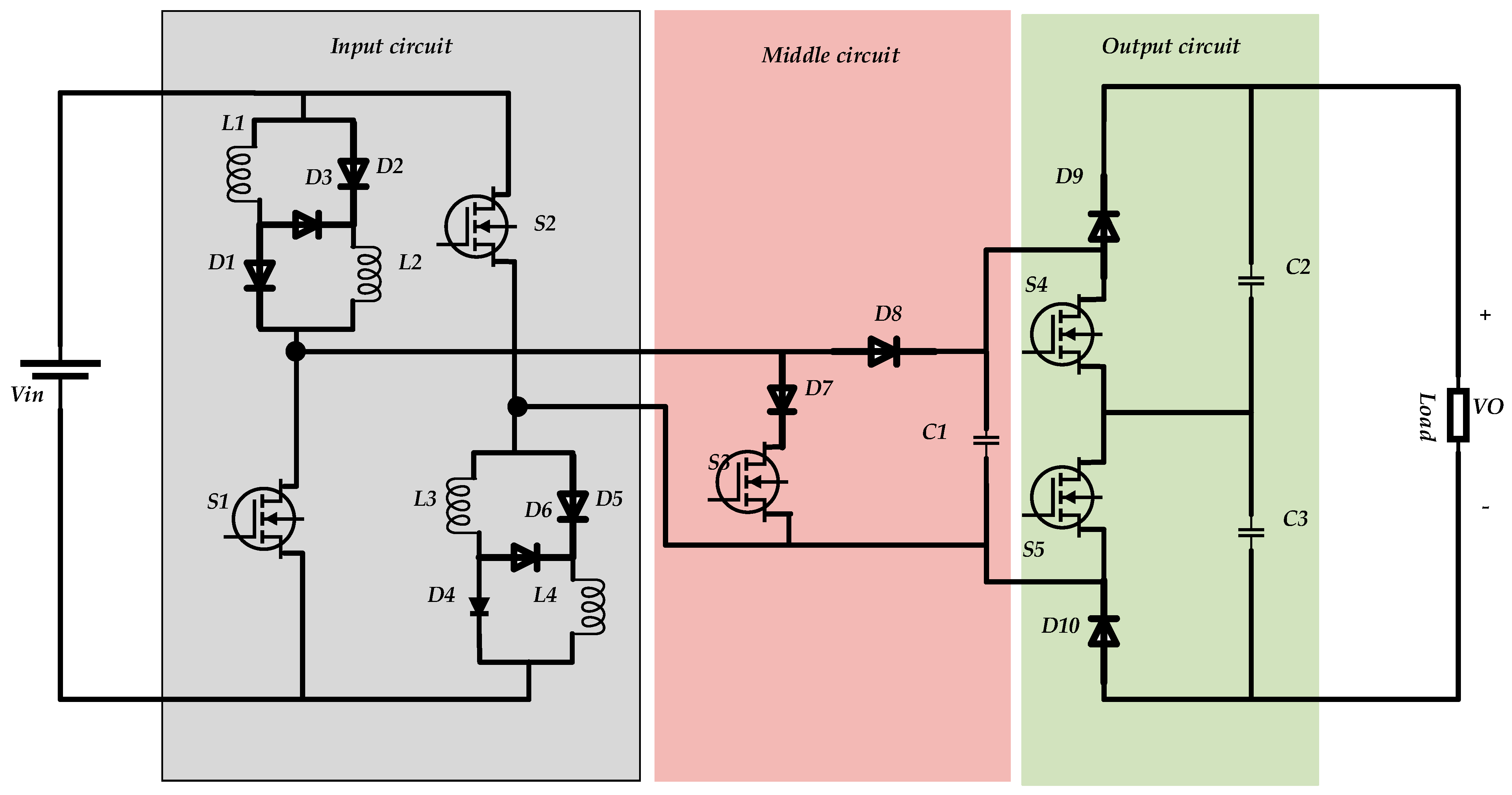
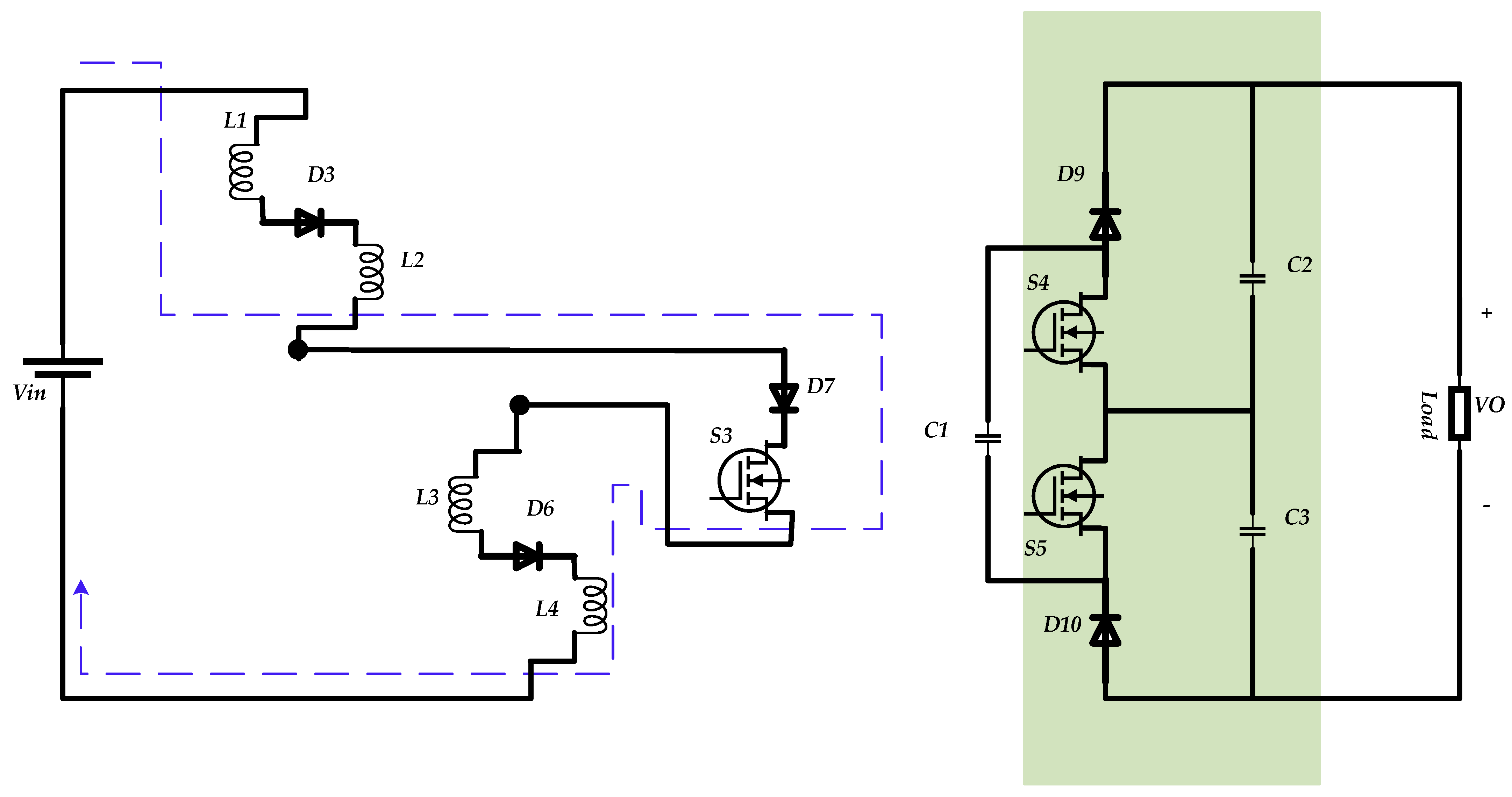
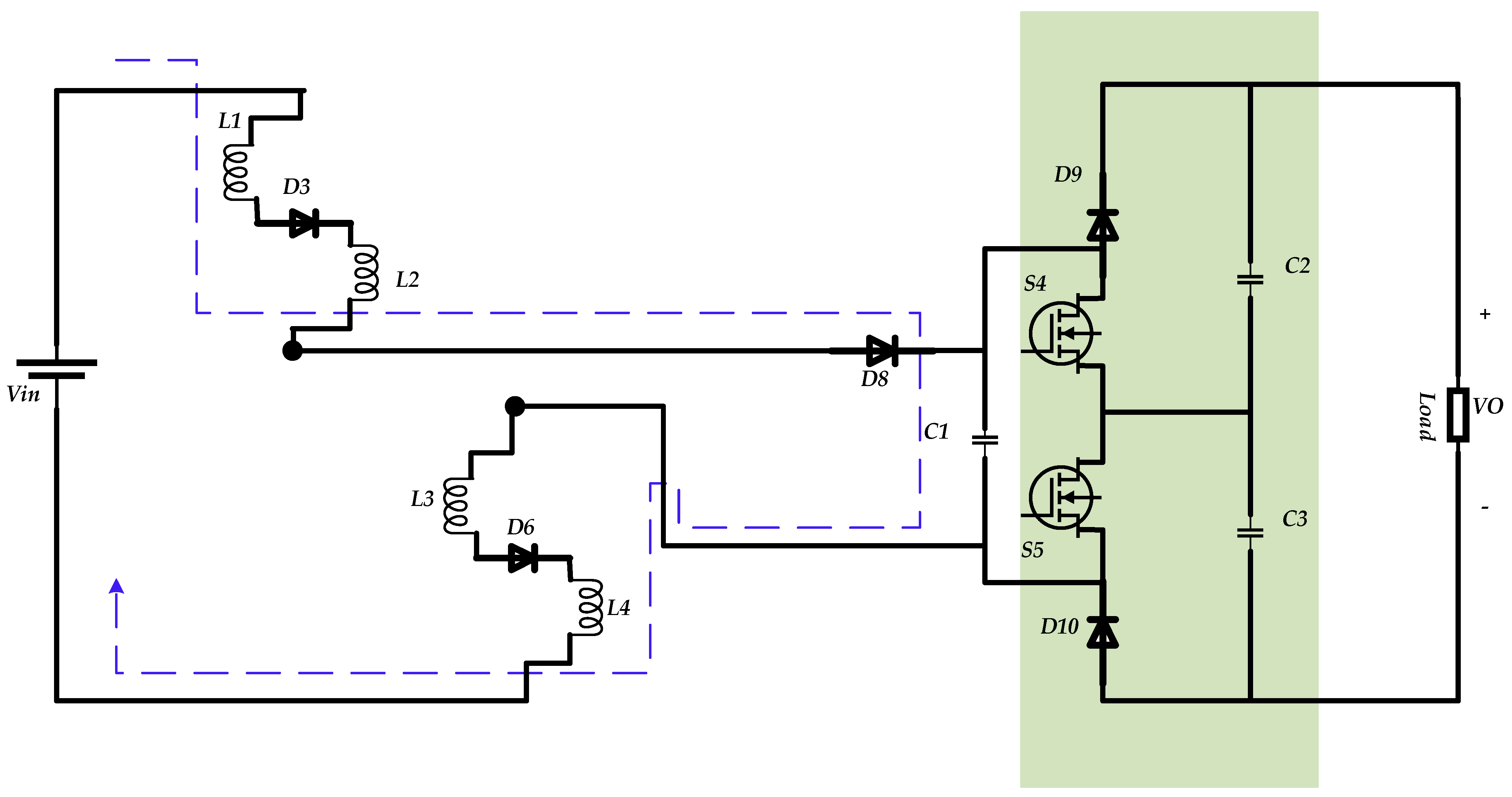
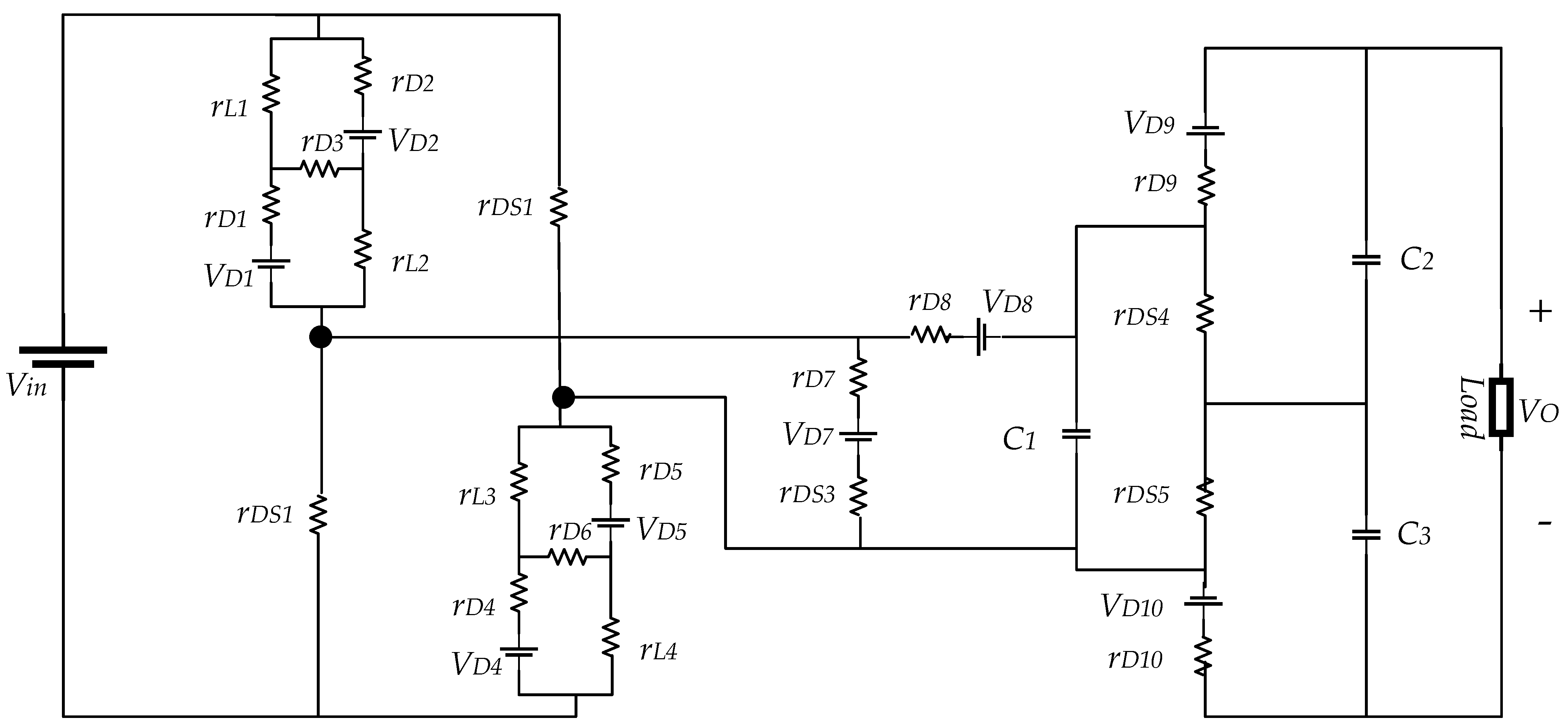
Figure 1 shows the proposed SL-SC-based boost converter. The structure of the converter can be analyzed in three sides: input, middle, and output. On the input side, two SL cells with the integration of the two switches can be seen. For the middle side, a conventional boost converter is selected. For the output side, an SC cell is used to double the generated voltage. The main idea for the SL cells has been taken from [31]. One of the most important features of a good converter is input currents with minimum ripples. The proposed SL configuration contains a pair of the same inductors that can be parallel or series through the power diodes. The main idea in the proposed circuit is that, for the time durations that the switches S1 and S2 are connected, these inductors with be parallel, which means four inductors are connected with the input voltage source in parallel and will be slowly charged, and they will be in series when the switches are disconnected. This means that the total amount of inductors per branch will be doubled, and this reduces the speed of the discharging process. All these details help the converter in minimizing the input current ripples. The details of this SL cell can be found in [31], and the state of the cell is reported in Figure 1, Figure 2 and Figure 3. In the body of the SL cells, two equal inductors and three diodes with the same specifications are used. Since both inductors are the same, they can be generated by using a core, which can easily decrease the cost and weight of the inductors. Both switches S1 and S2 are activated and deactivated simultaneously. This helps to easily investigate the equations for the input side.
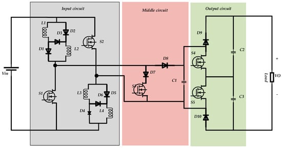
Figure 1.
The proposed SL-SC-based boost converter.
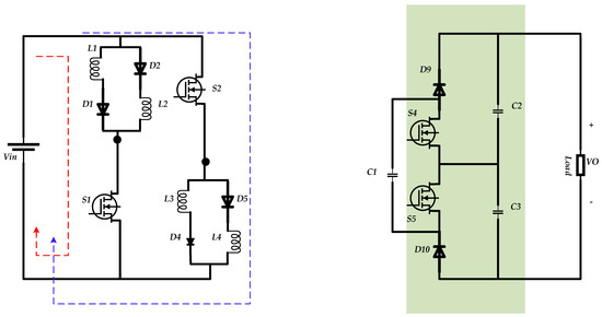
Figure 2.
The state of the converter for .
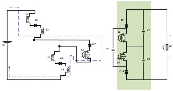
Figure 3.
The state of the converter for .
When the switches are in on-state, the inductors L1 and L2 from branch 1 and inductors L3 and L4 from the second branch are magnetized by the input voltage through the switches. In this state, the switch S3 is deactivated.
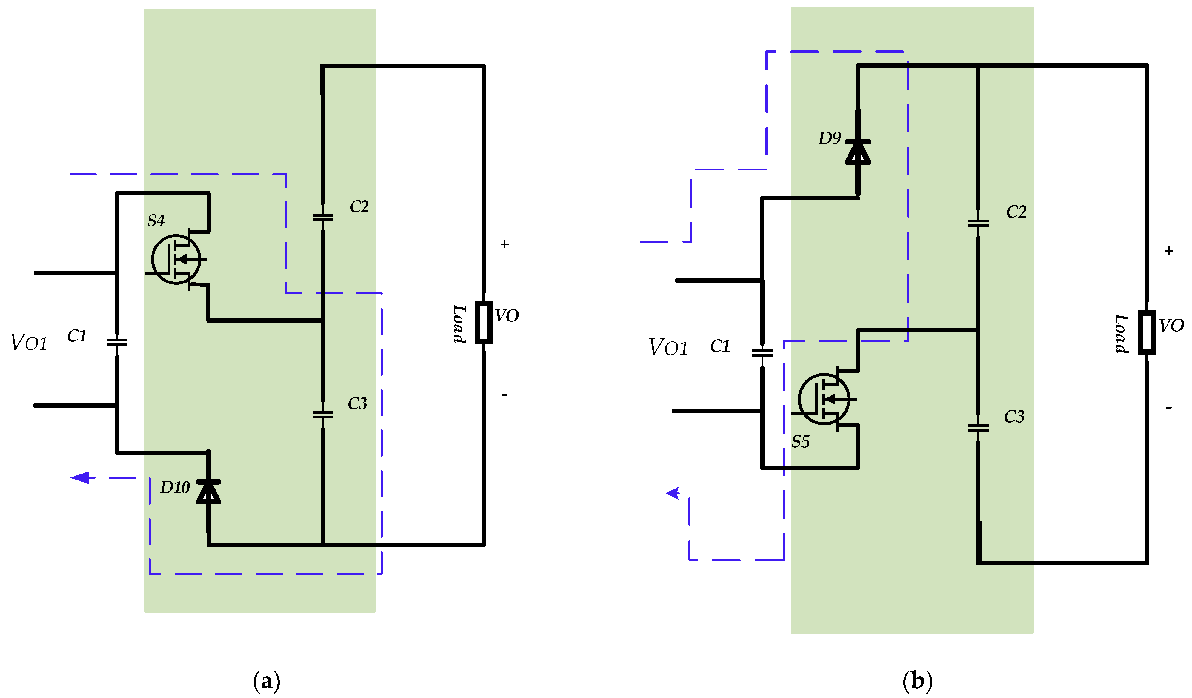
As can be seen, the same four inductors will act, and this helps to minimize the ripple for the input current in this state. When switches S1 and S2 are deactivated, switch S3 on the middle side will conduct. Under this condition, it is predictable that the diode D8 is in off-mode. In this operational mode, the current of the input side will pass through the inductors L1 and L2 in series and the diode D3, and after passing through the switch S3, it will complete the current loop through the inductors L3 and L4 and diode D6. In addition, a third mode is possible, which can happen when all switches in the input and middle sides are in the off-state. In this condition, the current form of the input source, after passing through the inductors L1 and L2 and diode D3, will receive diode D8, and as a result of this process, the capacitor C1 is charged. The voltage across the capacitor C1 will double by the output side, which can be followed in the yellow rectangular box. The circuit in this box acts separately and independently of the input and middle sides. This circuit is an SC-cell-based voltage lifter circuit and doubles the voltage across the capacitors C1. When the switch S4 is activated, a current from this switch passes through the capacitor C3 and diode D10, and a voltage equal to the VC1 drops across the capacitor C3. The same reaction can be seen when the switch S5 is activated. In the same working mode, the current of the diode D9 charges the capacitor C2. Finally, a doubled voltage of capacitor C1 is transferred to the load. Therefore, the reaction of the proposed converter can be analyzed in three different modes. All these states are presented in detail in Section 2.1.
2.1. Working Modes of the Converter and Gain Calculations
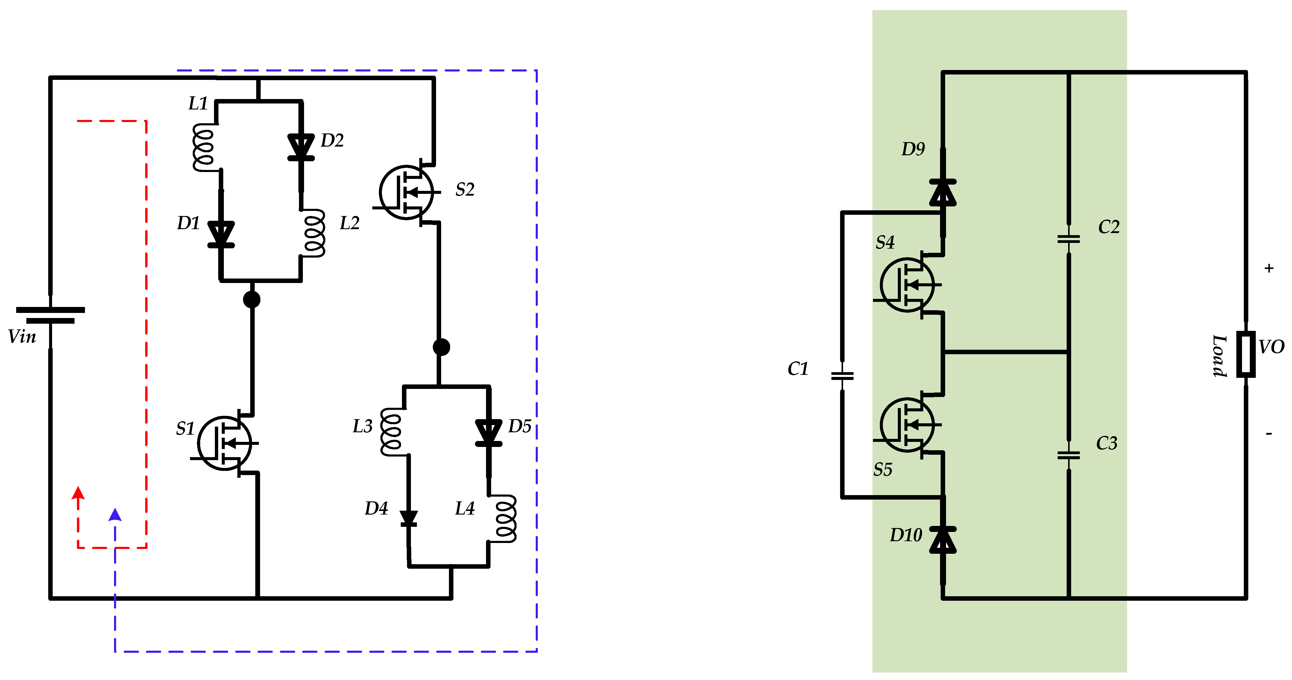
Mode I. The first possible working condition happens when both switches S1 and S2 are in the on-state. The time duration for this state is considered as . For this mode, diodes D1 and D2 in the upper SL cell and diodes D4 and D5 in the downer SL cell will be on, and the current of the input side will magnetize four inductors simultaneously. Therefore, one can write:
In this equation, are the inductance values of all inductors to and are the same. In addition, is the voltage across the inductors and is equal for all inductors, while presents the current for the inductors.
Therefore:
The state of the converter for this operational mode is shown in Figure 2.
Mode II. In the second mode, switches S1 and S2 are in off-mode, and switch S3 is activated. As can be seen in Figure 3, for this state, the input current follows through the inductor L1, diode D3, inductor L2, diode D7, switch S3, inductor L3, diode D6, and inductor L4. Since the voltage across the capacitor C1 is more than the voltage of the anode pins of the diodes D7 and D8, the diode D8 acts in off-state. The current and voltages for the inductors in this mode can be summarized as below:
The time duration for this mode can be considered as . and are the time intervals that the switches S1–S2 and S3 are activated, respectively.
Mode III. This mode happens for the times that all switches S1, S2, and S3 are in off-state. The configuration of the proposed converter under this working mode is illustrated in Figure 4, which shows that the input voltage can be transferred across the capacitor C1 with a voltage gain. The input and middle sides of the proposed circuit are parts of an improved and optimized boost converter, and the gain of this converter should be calculated.
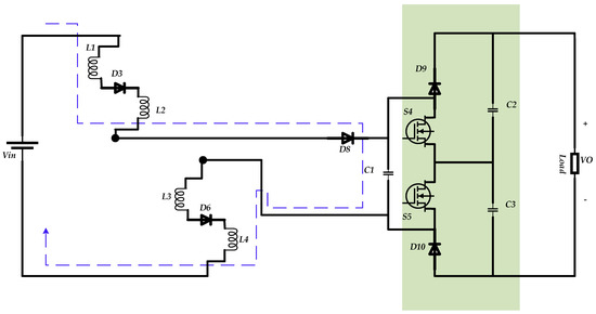
Figure 4.
The state of the converter for .
The current and voltages of the inductors for this mode can be written as follows:
Therefore:
indicates the voltage crosses the capacitor . These equations are valid for .
Equation (5) shows that for , the current derivation for the inductors is equal to . Equation (8) shows that this value for the time is equal to . In addition, for , as can be seen in Equation (11), this value is . By considering that the average voltage across an inductor is equal to zero, and paying attention to Equations (5), (8) and (11), one can write:
By a simple replacement in Equation (12), we can find the gain of the converter just across the capacitor and before the output voltage-doubler block (configurations between the capacitor and load) as follows:
shows the gain of the converter for the continuous conduction mode (CCM). This equation shows that for and , the gain of the converter is equal to 16.66, and a voltage at the input side equal to 12 V will convert to 200 V across the capacitor . This voltage will be gained to 400 VDC across the load. For longer duty ratios, greater gain values can be obtained. For example, with and , the proposed converter presents a voltage 50 and 100 times greater than the input voltage for SL and SL-SC-based converters, respectively. indicates the total gain of the converter by considering the SC cell.
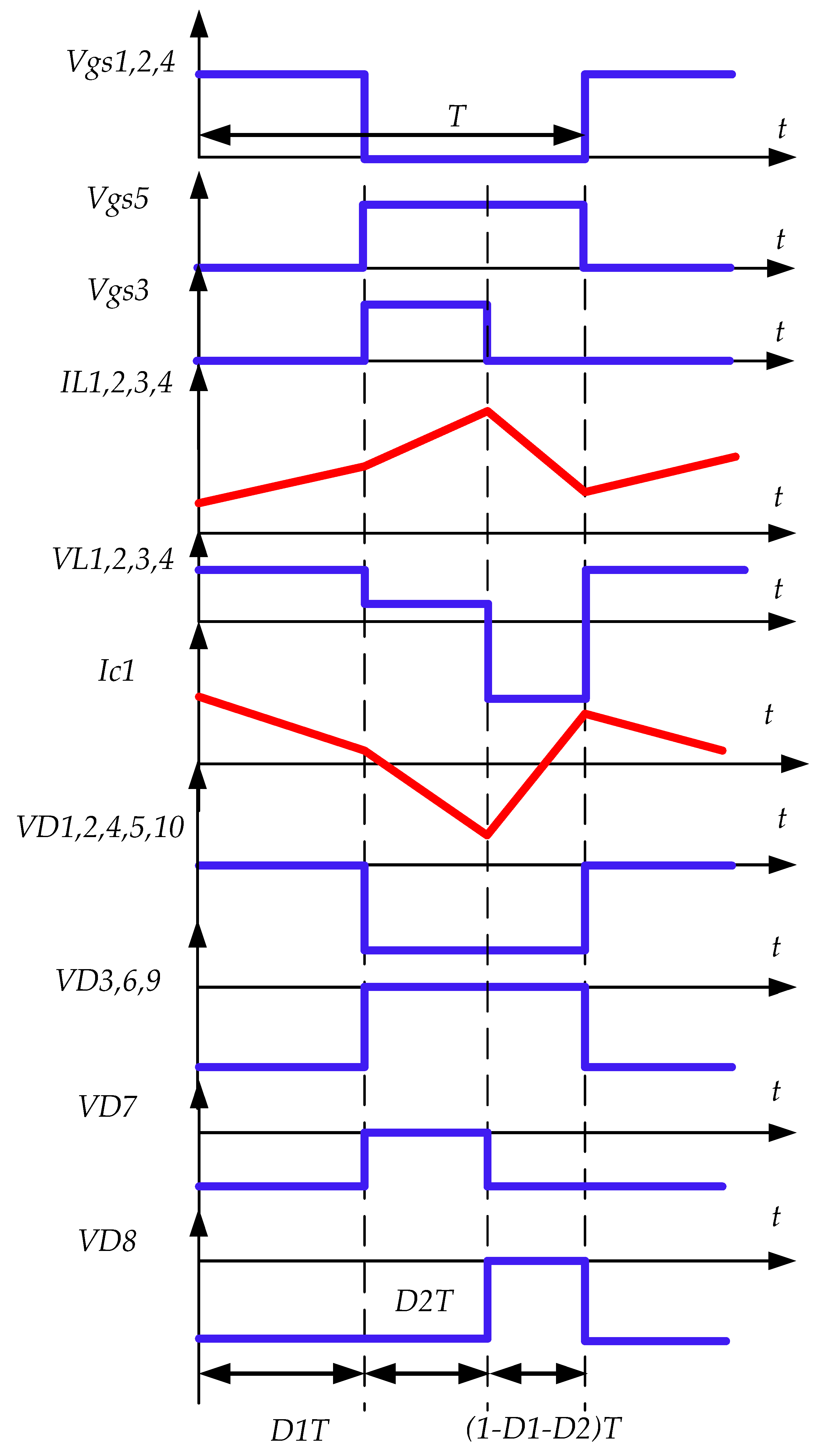
Figure 5 shows the integrated SC cell in the proposed converter. This circuit is a voltage-doubler configuration and transfers the voltage across the capacitor C1 to across the capacitors C2 and C3 by activating the switches S4 and S5, respectively. Therefore, a voltage equal to appears on the load. This simple topology can work with different duty ratios and different switching frequencies. To obtain a simple control circuit, the same switching frequency and the same deriving signal for switches S1 and S2 can be used for switches S4 and S5, respectively. The predicted voltage and current waveforms for the proposed converter can be seen in Figure 6. The voltage across the gate-source pins of the power switches, the voltage across the anode-cathode pins of the power diodes, and the current of the inductors and output capacitor can be followed in this figure. Accurate values of these voltages and currents will be calculated in the next subsections.
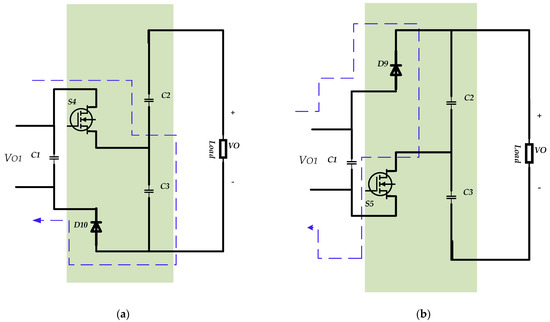
Figure 5.
(a,b) The SC-based voltage lift circuit and state of the switches and diodes.
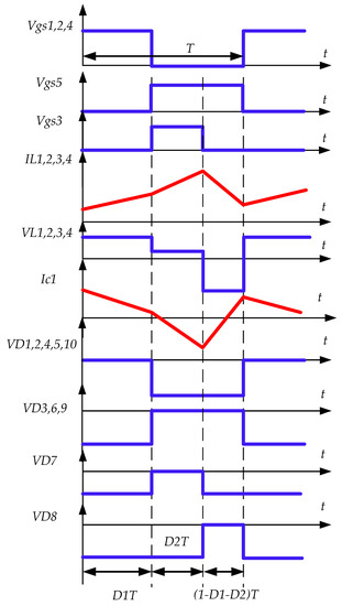
Figure 6.
Voltage and current waveforms for the components of the proposed converter.
2.2. Voltage Stresses across the Semiconductor Devices
The voltage stress for the switches S1, S2, and S3 can be presented as follows:
For solving these equations, the state of the switches should be considered for time intervals in which the same switches are in the off-state as in modes II and III. Then, the voltage at the drain and source pins should be considered.
By a similar model, the voltage stress across the diodes on the input side can be found:
These voltages for the middle-side elements and are equal to:
For semiconductor elements at the output side, the voltage stress across the diodes D9 and D10 and the switches S4 and S5 can be obtained by the following:
2.3. Current Stresses of the Inductors
For working under the CCM, the currents of the inductors can be written as below:
In this equation, is the minimum value of the inductor for working at the boundary (BCM) between the continuous and discontinuous conduction modes. In practice, to work under CCM, an inductor greater than the calculated value in this equation should be considered. The coefficient for the is close to 1.25. This equation shows that the inductor value is dependent on the input voltage value, the duty ratio for the switches S1 and S2, the ripple of this current, and the switching frequency. This means that for fewer ripples and smaller inductor values, an increment in the switching frequency can be a good idea. In addition, in this way, the size, volume, and cost of the inductor will decrease.
2.4. Capacitor Design
The voltage ripple across the capacitor C1 depends on the value of this capacitor, the duty ratio of the switch D3, the switching frequency, and the output load. Therefore, this ripple can be modeled as follows:
3. Working with Non-Ideal Components (Real Condition)
This subsection aims to present the efficiency equation for the proposed converter. For this, the current for the capacitor C1 and the voltage across the input inductors should be obtained for all three possible modes. These calculations will be done by considering the internal resistances of the inductors, diodes, and switches, and the forward voltage of the power diodes. Figure 7 shows the state of the converter for efficiency calculations.
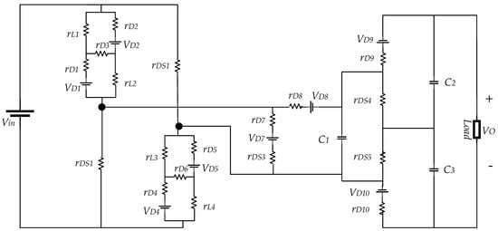
Figure 7.
Internal parameters of the diodes and switches for efficiency calculation.
Since the SC-cell doubles the voltage on capacitor C1, to simplify the equations, the SL and boost cells of the converter are considered, and then the effect of the voltage lifter side is investigated. A simplified configuration of the proposed converter can be seen in Figure 8. In both Figure 7 and Figure 8, the indicate the internal resistance of the inductors and respectively. The internal resistance of the diodes to is shown by to and the forward biasing voltage of these diodes is shown by to . Finally, the drain-source internal resistances are shown with to respectively, for switches to . By considering the same diodes and switches, we obtain the following:
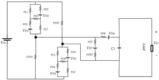
Figure 8.
Internal parameters of the diodes and switches of the input and booster sides.
For mode I, as can be followed, the switches S1 and S2 are in the on-state and S3 is in the off-state. In this state, the capacitor’s current and inductor’s voltage equations are:
For the second working mode, these equations can be found by:
For the third operational mode, they can be found by:
The current-second balance rule for a capacitor is written to show that the average current of the capacitor is equal to zero for a time period. By considering Equations (27), (29), and (31), the following can be written:
The current can be obtained as follows:
In addition, the voltage-second balance rule indicates that the average voltage across an inductor is zero for a time period. Therefore, by using Equations (28), (30) and (32), one can write:
By replacing and in Equation (35) and simplifying, one obtains:
To obtain the input power for the proposed converter, one can write:
By replacing Equation (34) into (36), one obtains:
In addition, the output power can easily be obtained as follows:
Therefore, the efficiency equation theoretically can be obtained by:
Besides the dynamic losses, the switching losses should also be considered for the semiconductor devices. This parameter is shown by in Equation (40). For the switches, this loss can be presented as:
where and are the switching frequency and parasitic capacitor for the drain-source pins of the switch, and shows the voltage drops across the switch when it is deactivated. The switching losses for the diodes can be presented by:
In this equation, , , and show the forward voltage for the diodes to activate, electrical charge across the parasitic capacitor between anode-cathode pins, and switching frequency, respectively. The total power losses for the switching states can be obtained as follows:
4. Analysis, Simulation, and Experimental Results
4.1. Comparison with Similar Converters and Performance Investigation
For a safe comparison, Table 1 presents several DC-DC boost converters including switched-capacitor or switched-inductor cells. This table presents some of the features of the proposed converters. For example, the number of power switches, diodes, inductors, and capacitors; the voltage stress on the main power switch; and the voltage gain are compared. From this table, it can be seen that the number of switches for the proposed converter and the structures proposed in [32] and [33] is the same, and the number of switches in the proposed converter is higher than the number of switches for the converters in [29,34,35]. While the proposed converter in this study includes the highest number of inductors and diodes, it also includes the lowest number of capacitors and presents the greatest voltage gains. The gain value by the proposed converter is perceptibly higher than other converters. This is possible thanks to the higher number of elements. Some of the elements in this converter can be integrated. For example, since all of the inductors have the same specifications, they can be wrapped with a common core. This means that instead of four separate inductors, two pairs of coupled inductors for the L1-L2 and L3-L4 inductors can be used. This integration will lighten the converter, and the cost of inductors will be almost halved. Under this condition, the proposed converter will have the same number of inductors as the converters in [29,32,33,34,35], the same number of switches as the converters in [32], and the same number or fewer capacitors than all these converters. Only the number of diodes will be higher than the other compared converters, which can be ignored by considering the gain of the converter.

Table 1.
Feature comparison between the proposed and other SL-SC-based converters.
Table 1.
Feature comparison between the proposed and other SL-SC-based converters.
| Converter | No. of Switches | No. of Inductors | No. of Diodes | No. of Capacitors | Voltage Stress across the Switch | Voltage Gain | Gain at D = 0.5 |
|---|---|---|---|---|---|---|---|
| [29] | 1 | 2 | 5 | 4 | 7 | ||
| [32] | 3 | 2 | 2 | 1 | 5 | ||
| [33] | 3 | 2 | 0 | 1 | 3 | ||
| [34] n = 1 | 1 | 1 + 1 coupled inductor | 5 | 3 | 6 | ||
| [35] | 1 | 3 | 4 | 4 | 6 | ||
| Proposed | 3 | 4 or 2 coupled inductor | 8 | 1 | 16.66 |
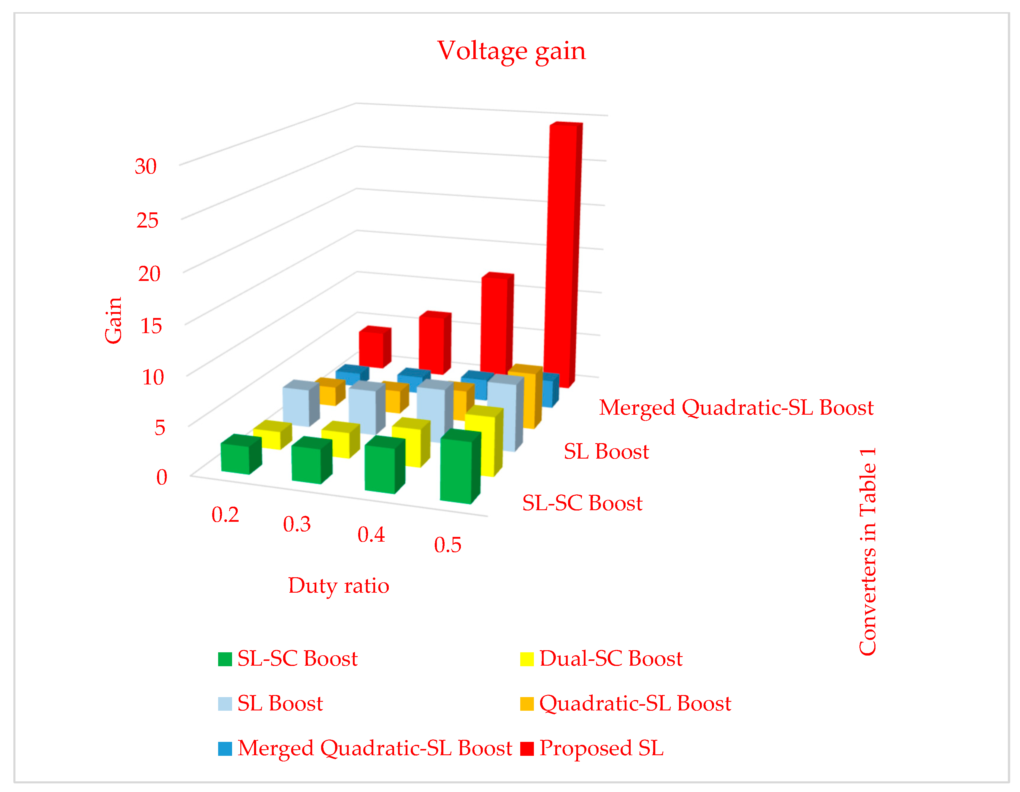
In order to present the results of Table 1 visually, some figures, curves, and diagrams are presented. Figure 9 and Figure 10 illustrate the gain of the suggested converters in Table 1. Figure 9 presents the gain for the shorter duty ratios, and Figure 10 shows the results of the gain comparison for the longer duty ratios. Since the converters in [32] and those in this study have two different duty ratios, the second duty ratio is considered equal to for Figure 9 and for Figure 10. Both these figures have been drawn without considering the SC-cell. By adding the SC block, the presented voltage gains will double.
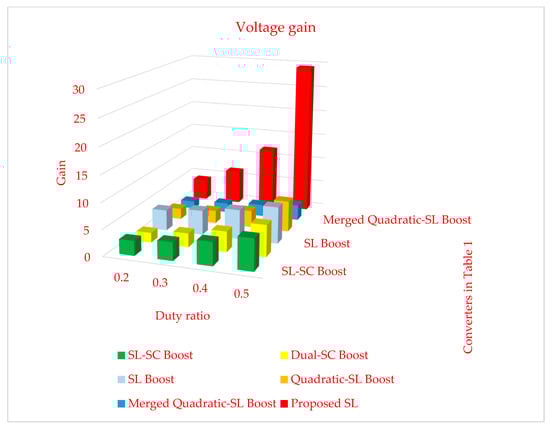
Figure 9.
Voltage gain comparison for shorter duty ratios.

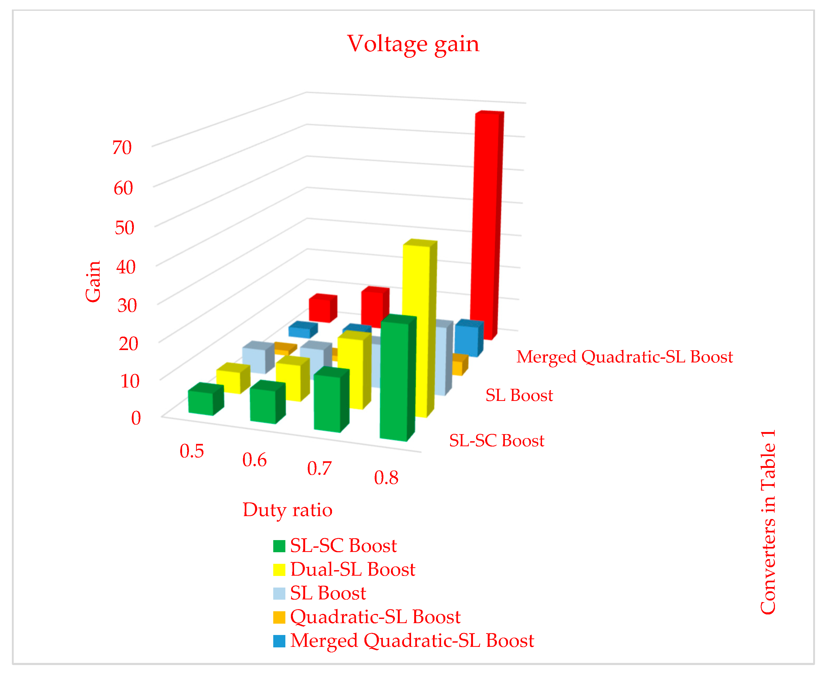
Figure 10.
Voltage gain comparison for longer duty ratios.
As can be seen for the smaller duty ratios, the gain of the proposed converter is higher. As is known, an appropriate converter is expected to work under shorter duty ratios. The reason for this is to obtain fewer power losses. Longer duty ratios mean longer activation time intervals for the semiconductor devices, which directly decreases the efficiency. Therefore, for a logical value of the duty ratio close to D = 0.5, the proposed converter, by presenting a voltage for the load that is 30 times greater than the input voltage, presents the best performance.
In addition, to show the reaction of the converters to longer duty ratios, Figure 10 is presented. Among all other converters, the circuit in [34] has a comparable performance in comparison with the converter suggested in this study. To draw these figures, the duty ratio of switch S3 is chosen as D2 = 0.416.
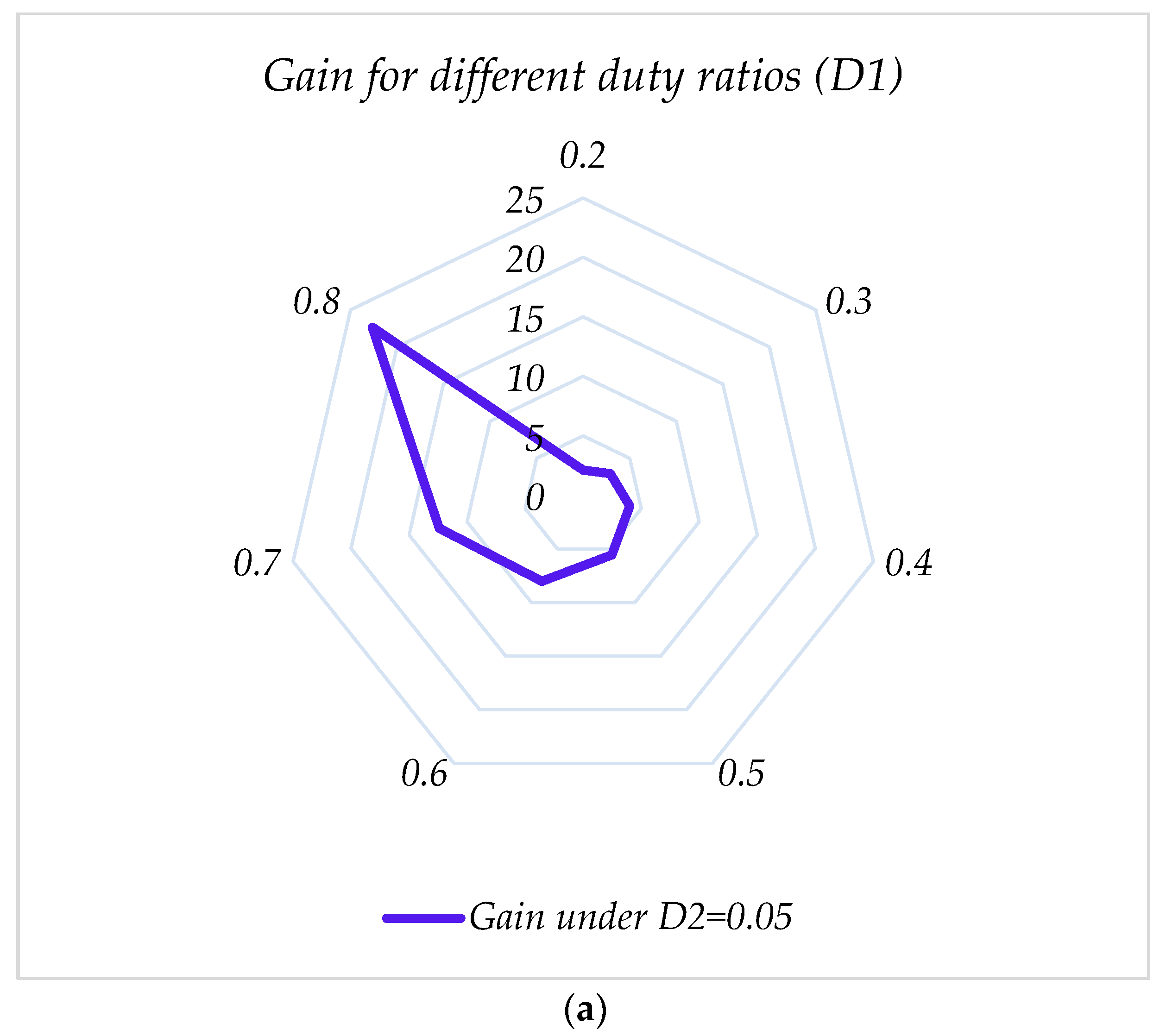
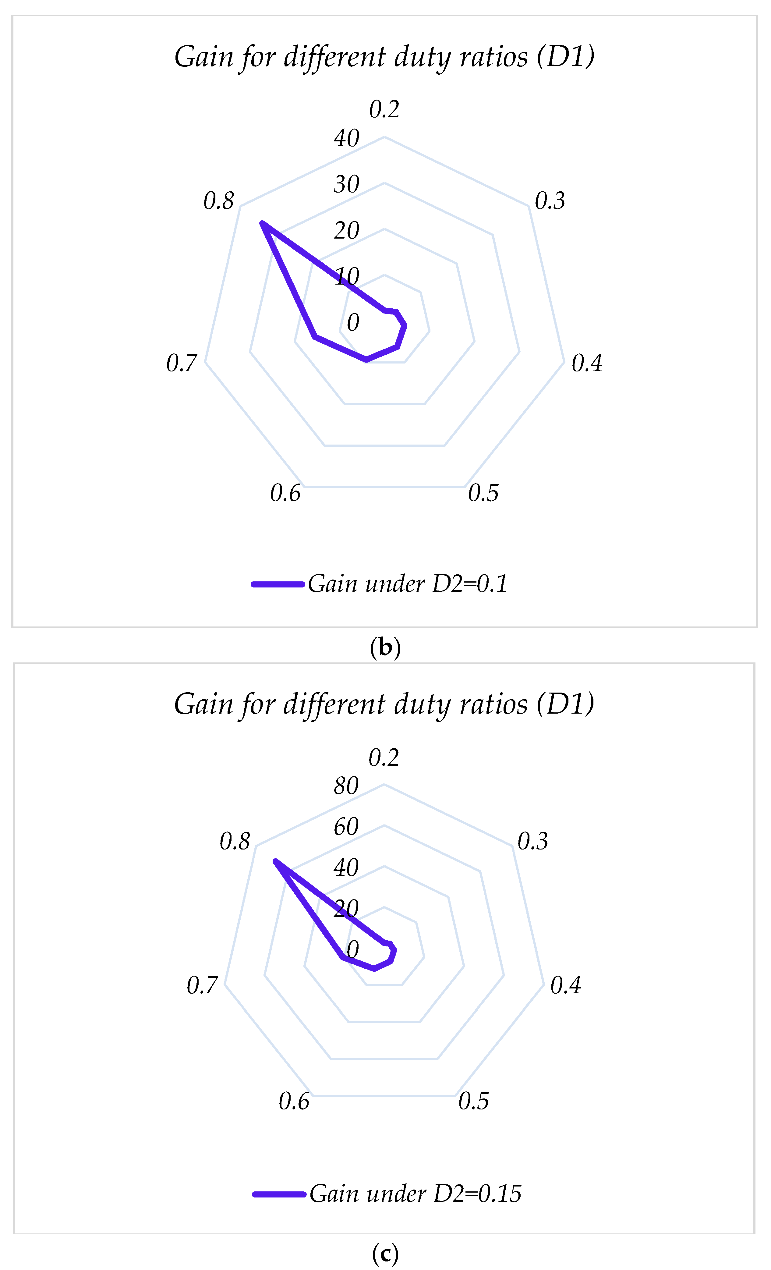
Figure 11 illustrates the gain of the proposed converter for different duty ratios of D1 and D2 for switches S1-S2 and S3. Figure 11a–c presents the gain curves for the duty ratios D2 = 0.05, 0.1, and 0.15, respectively. For all these curves, D1 changes from 0.2 to 0.8, and the gain of the converter is investigated. According to the results, for longer D2 time intervals, larger gains are obtained. All these figures have been drawn without considering the switched-capacitor cell.
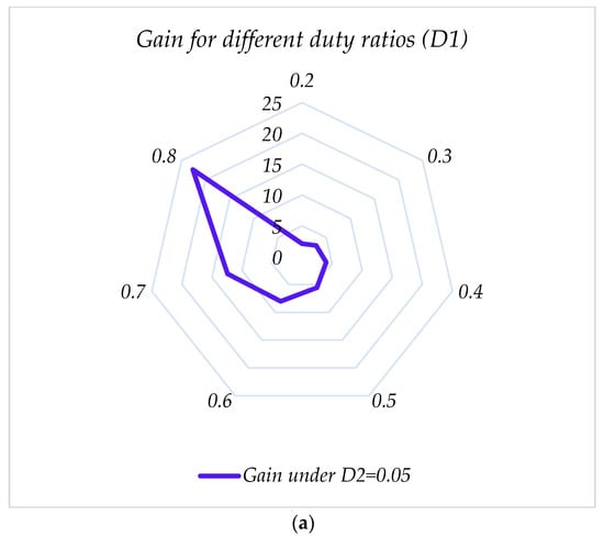
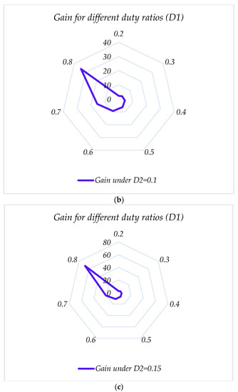
Figure 11.
Voltage gain for the proposed converter with (a) , (b) , and (c): , without considering the SC-cell effect.
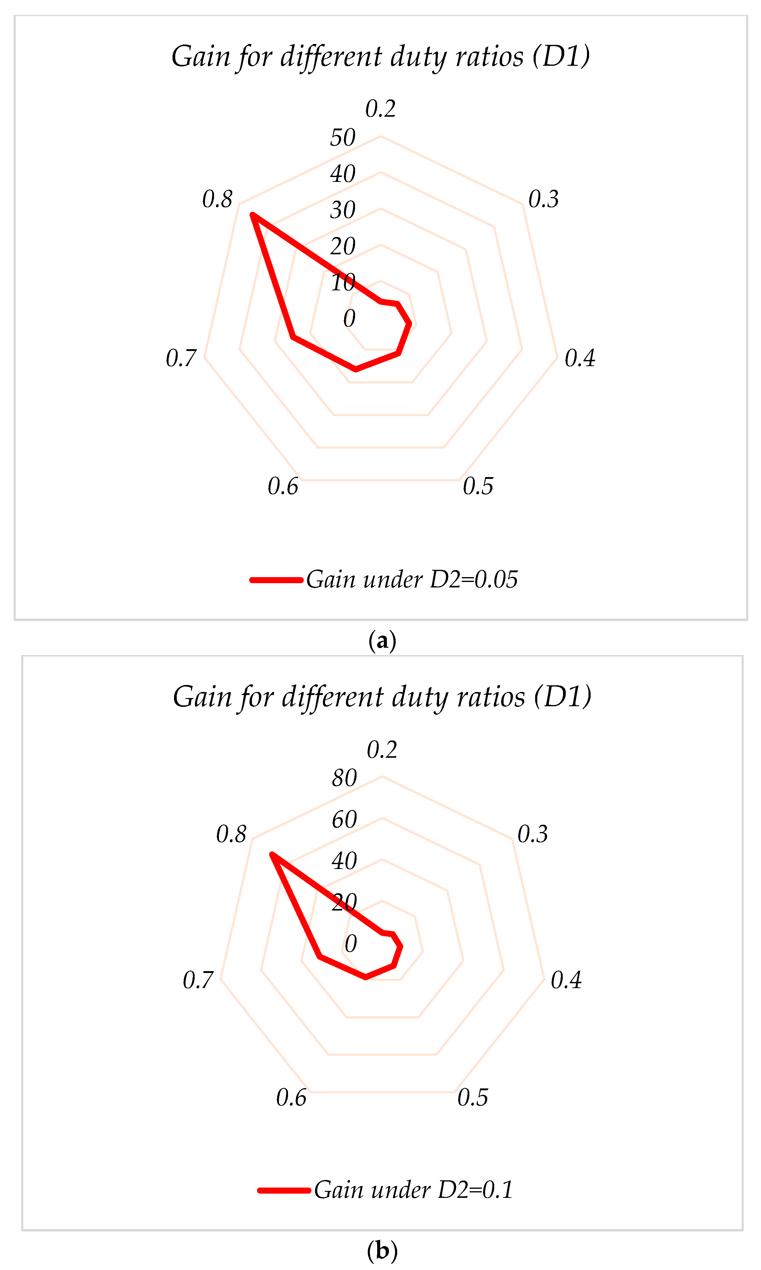
Figure 12a–c shows the gain of the converter considering the effect of the SC-cell. As mentioned, this block is considered to simply double the voltage across the capacitor C1 and is advised for the low-voltage working condition. With this cell, a greater voltage can be reached by the load.
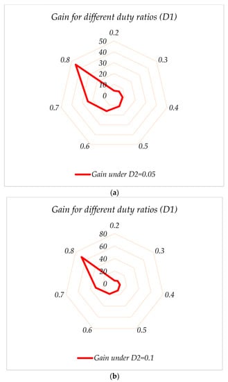
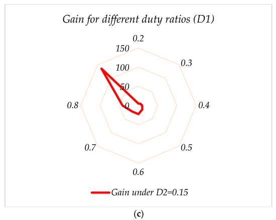
Figure 12.
Voltage gain for the proposed converter with (a) , (b) , and (c) , considering the SC-cell effect.
4.2. Simulation Results
A group of simulation results is presented in this section. For the simulation, and based on the presented equations in Section 2, the values of the components are chosen as shown in Table 2.
Table 2.
Parameters values.
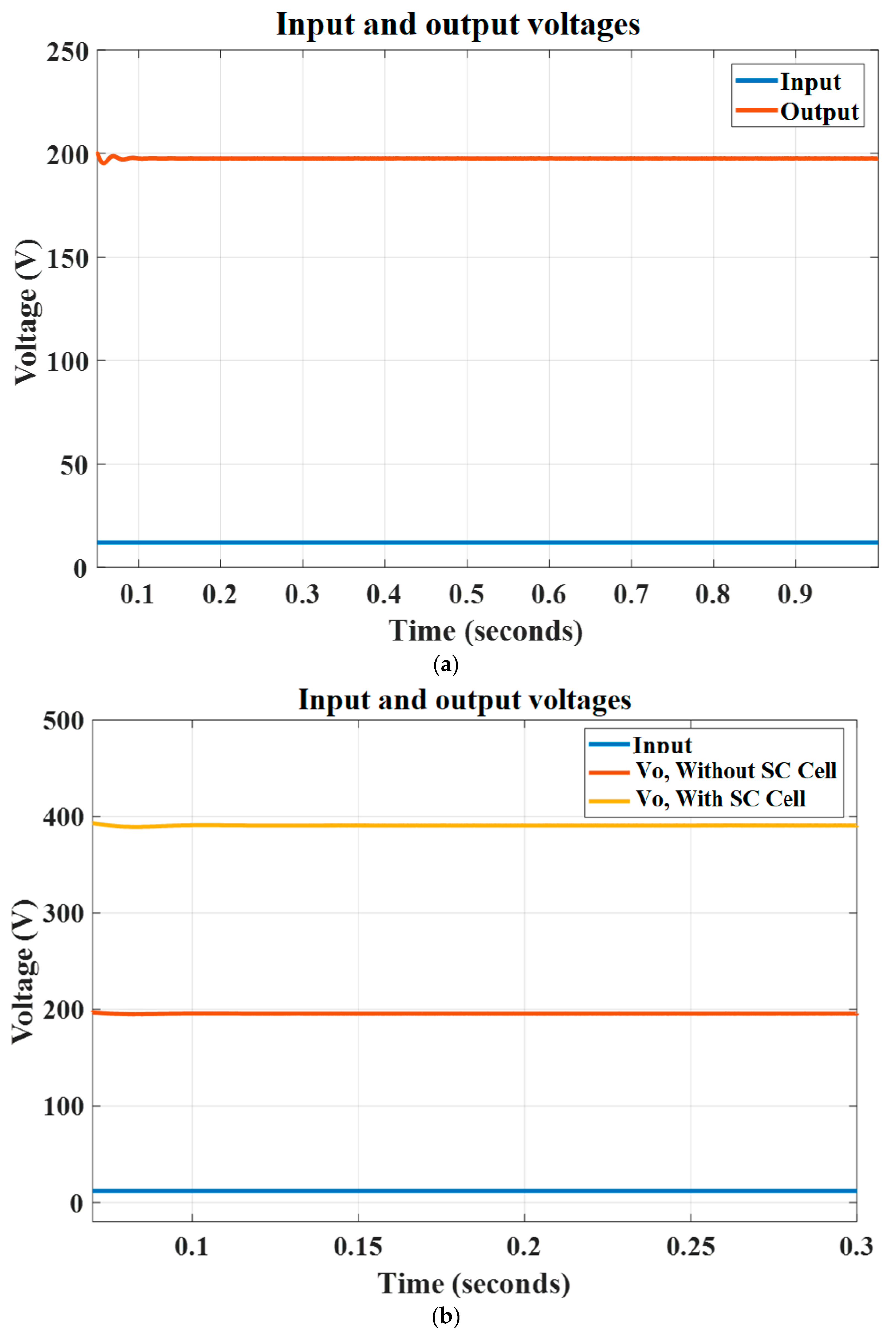
Simulation results are presented in Figure 13. The input and output voltages are shown in Figure 13a. The input voltage value is adjusted to 12 VDC, and a voltage close to 200 VDC across the capacitor C1 is obtained. This voltage can be considered as the input voltage for the SC-cell, and in total, a gain equal to 33.33 and 16.66 is obtained with and without the SC-cell, respectively.
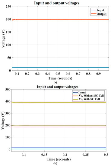
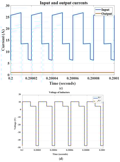
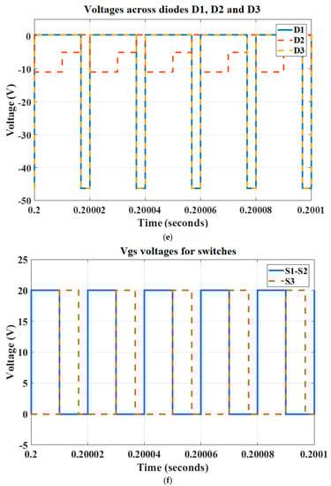
Figure 13.
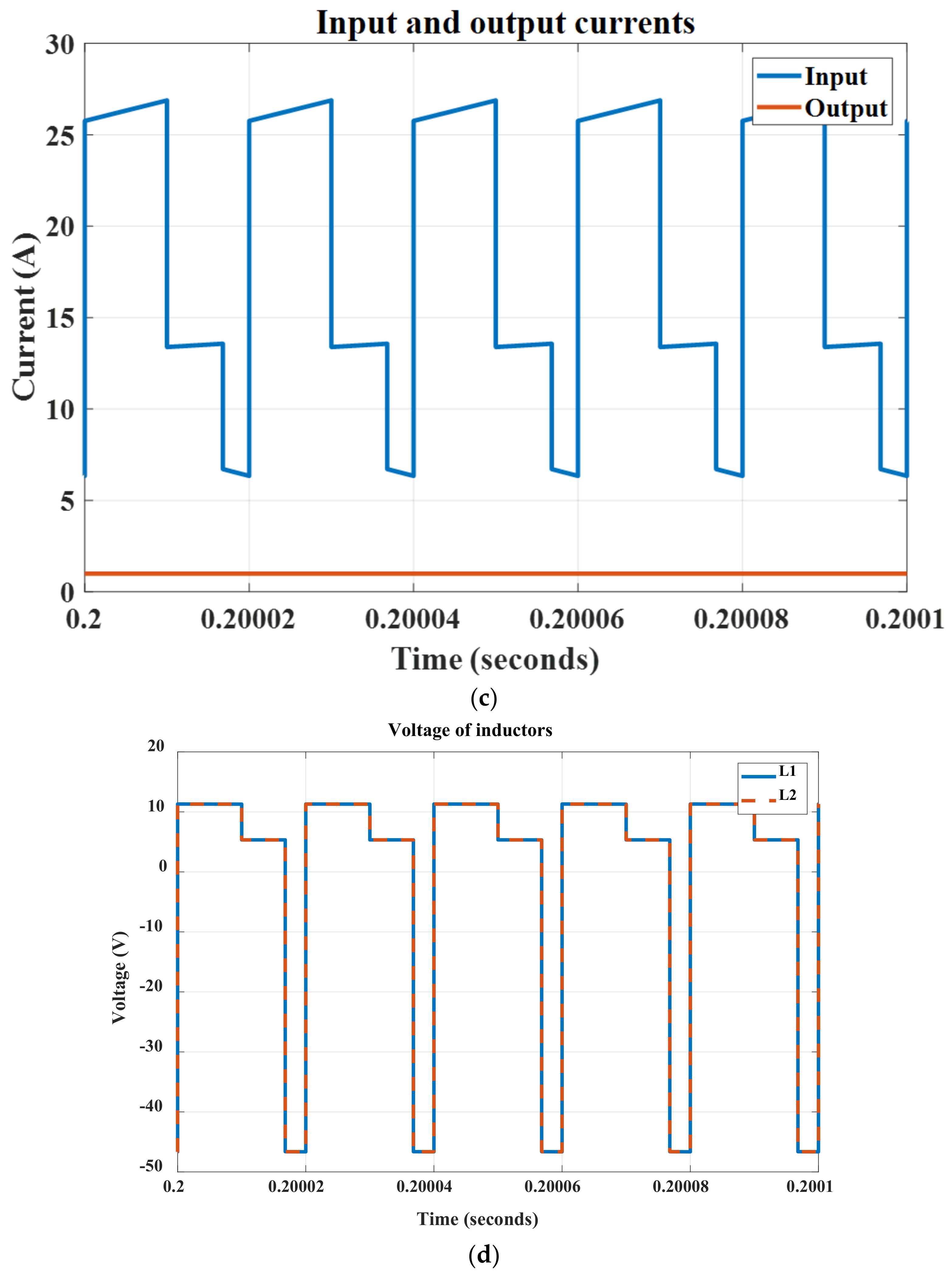
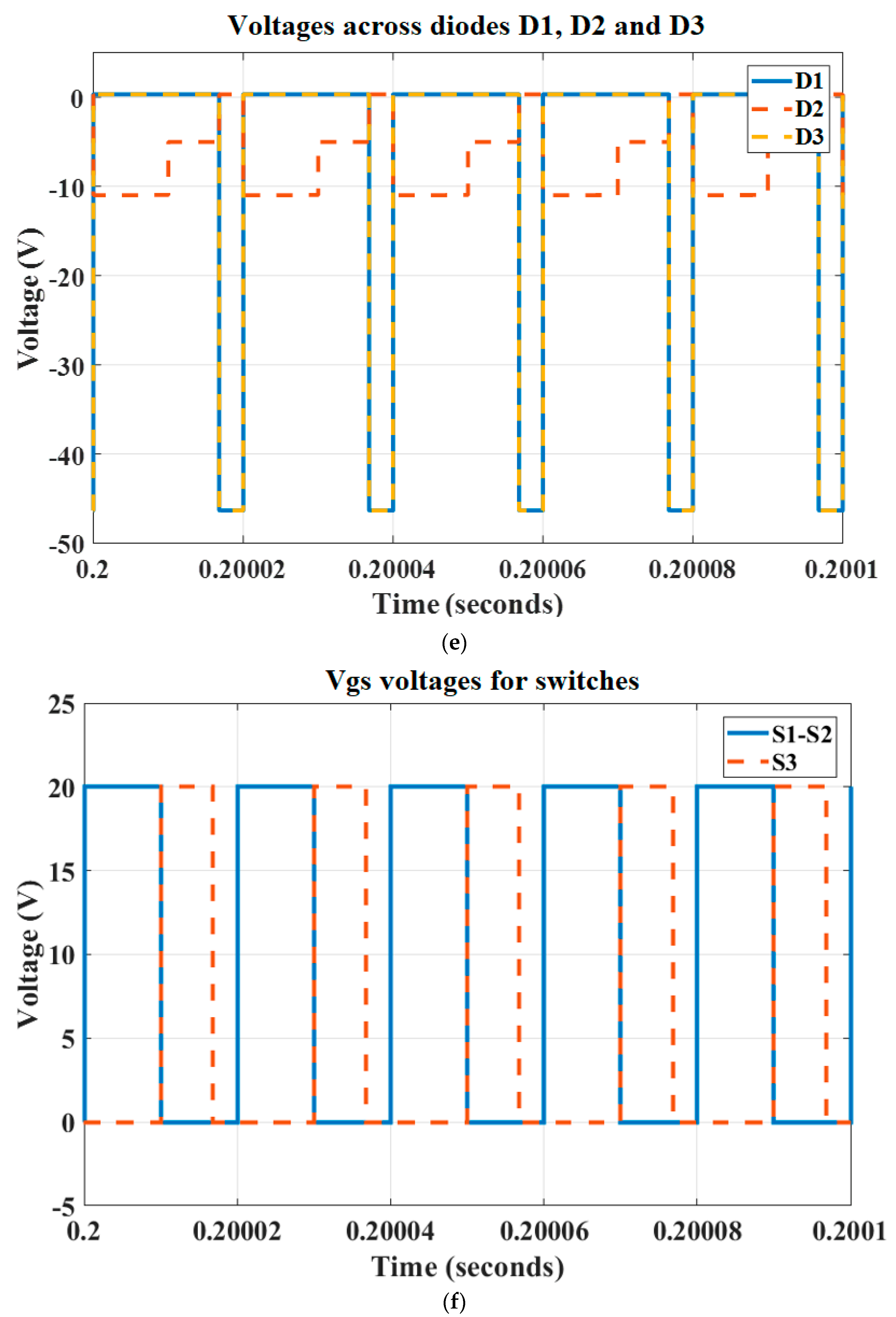
Input-output voltages (a) without and (b) with SC-cell, (c) input-output currents, (d) voltages across the inductors, (e) voltage of diodes D1 to D3, and (f) switching signals for the switches.
For this figure, the duty ratios for D1 and D2 are considered as D1 = 0.5 and D2 = 0.416. Figure 13a presents the output voltage of the capacitor C1 without application of the SC-cell. The effect of the SC-cell can be seen in Figure 13b. Figure 13c presents the input and output currents. Since the experimental test results are considered for a 200 W prototype circuit, the simulation analysis is done for this rated power for a fair comparison. For this power value, a current close to 1 A at the load side and an average value close to 16.66 A for the input source are expected. Figure 13c shows that the circuit reflects these values thoroughly.
The voltage across the inductors is shown in Figure 13d. Since the same reaction is expected for the inductors L3 and L4, the voltage for the inductors L1 and L2 is reported. This figure thoroughly shows that both inductors are magnetized and demagnetized synchronously. According to the second-balance voltage rule for an inductor in a switching circuit, the average voltage across the inductor is zero in a switching period. This figure shows that this rule has been obtained for the inductors correctly in the proposed converter topology.
Another expected voltage waveform is reflected in Figure 13e. The voltages across the diodes D1 and D2 are zero and negative synchronously, and the diode D3 is activated for the time intervals that the diodes D1 and D2 are deactivated and vice versa. This figure shows that the SL cell is working correctly.
The voltage across the gate-source pins for switches S1 to S3 can be seen in Figure 13f. This figure shows that the switches S1 and S2 are in on- and off-states simultaneously, and switch S3 only is activated for a short time when these switches are in the off-state.
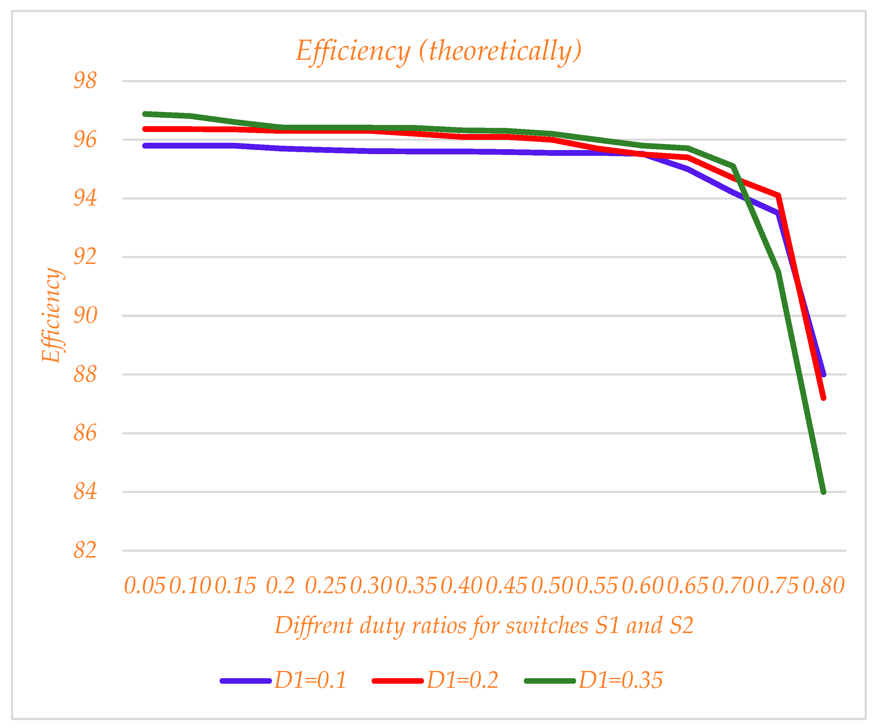
The efficiency of the converter is presented for different values of D1 and D2 theoretically for the proposed converter in Figure 14. For this, a group of curves is presented without considering the effect of the SC-cell for and , and then in Figure 15, the effect of the SC block is considered, and the curves are redrawn.
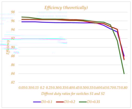
Figure 14.
Efficiency diagram for , and different values, without considering the SC-cell effect.
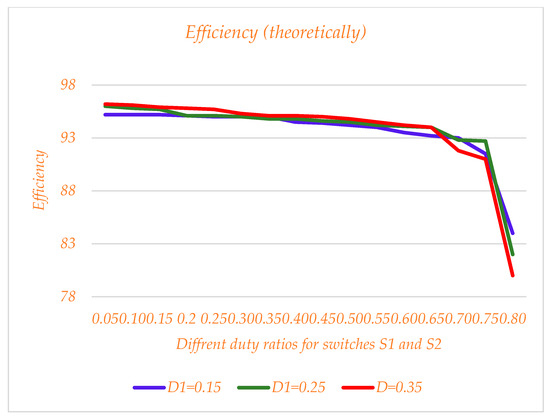
Figure 15.
Efficiency diagram for and different values, considering the SC-cell effect.
4.3. Experimental Results
To verify the simulation and theoretical results, a group of hardware tests has been performed, and the results are presented in this subsection. According to the simulation results, for a fair comparison, a 200 W prototype converter circuit was established in the laboratory, and different voltages and currents were measured. The elements have been selected based on the values in Table 1. The input voltage is adjusted on 12 VDC, and the output voltage is measured with and without considering the SC-cell. The switching frequency for all switches is adjusted to 50 kHz. A TP65H035G4WS type of the Super GaN, n-channel power MOSFET, with maximum 41 mΩ internal resistance and ability to bear 650 V across the drain-source pins, is selected for the power switches.
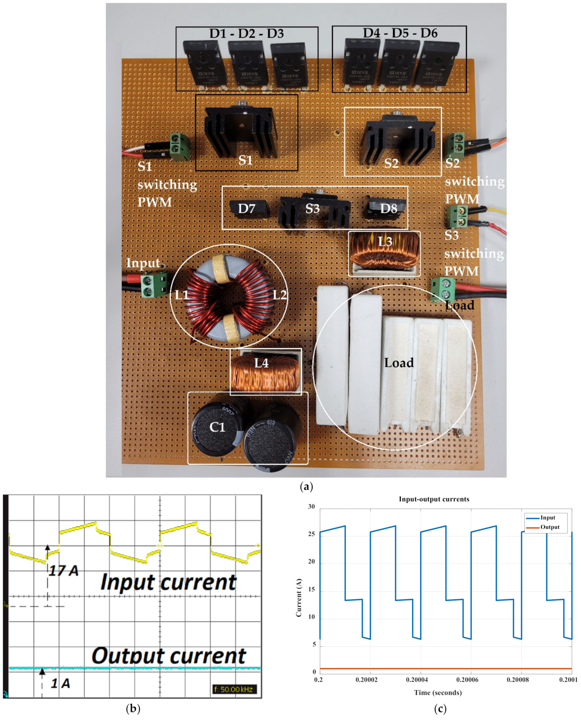
For the diodes, the DSEP30-06 super barrier rectifier power diode, with 1.25 V as the maximum forward biasing voltage and 30 A as the forward current, is selected for fewer power losses and higher performance. The duty ratio for switches S1 and S2 is D1 = 0.5 and for the switch S3 is D1 = 0.35, according to Table 2, to obtain a voltage equal to 200 V for the load without considering the SC-cell effect. All of the inductors and capacitors have the same value, which is equal to 400 µH and 100 µF, respectively. Figure 16a presents the prototype hardware circuit.
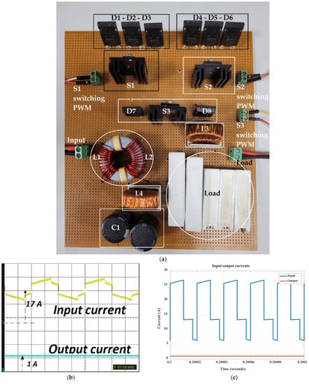
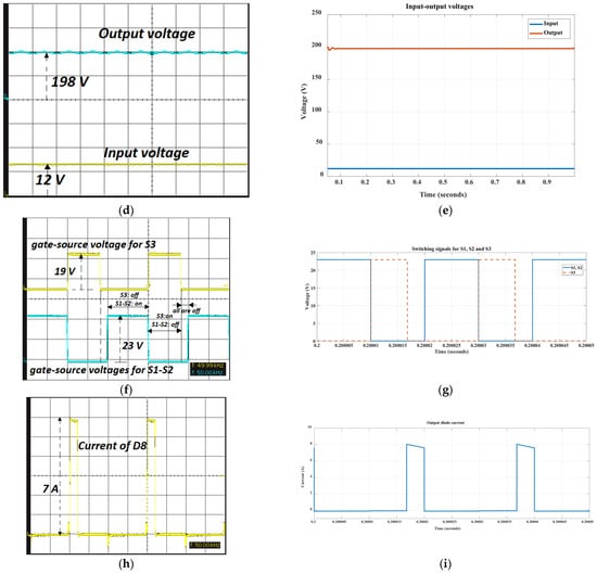
Figure 16.
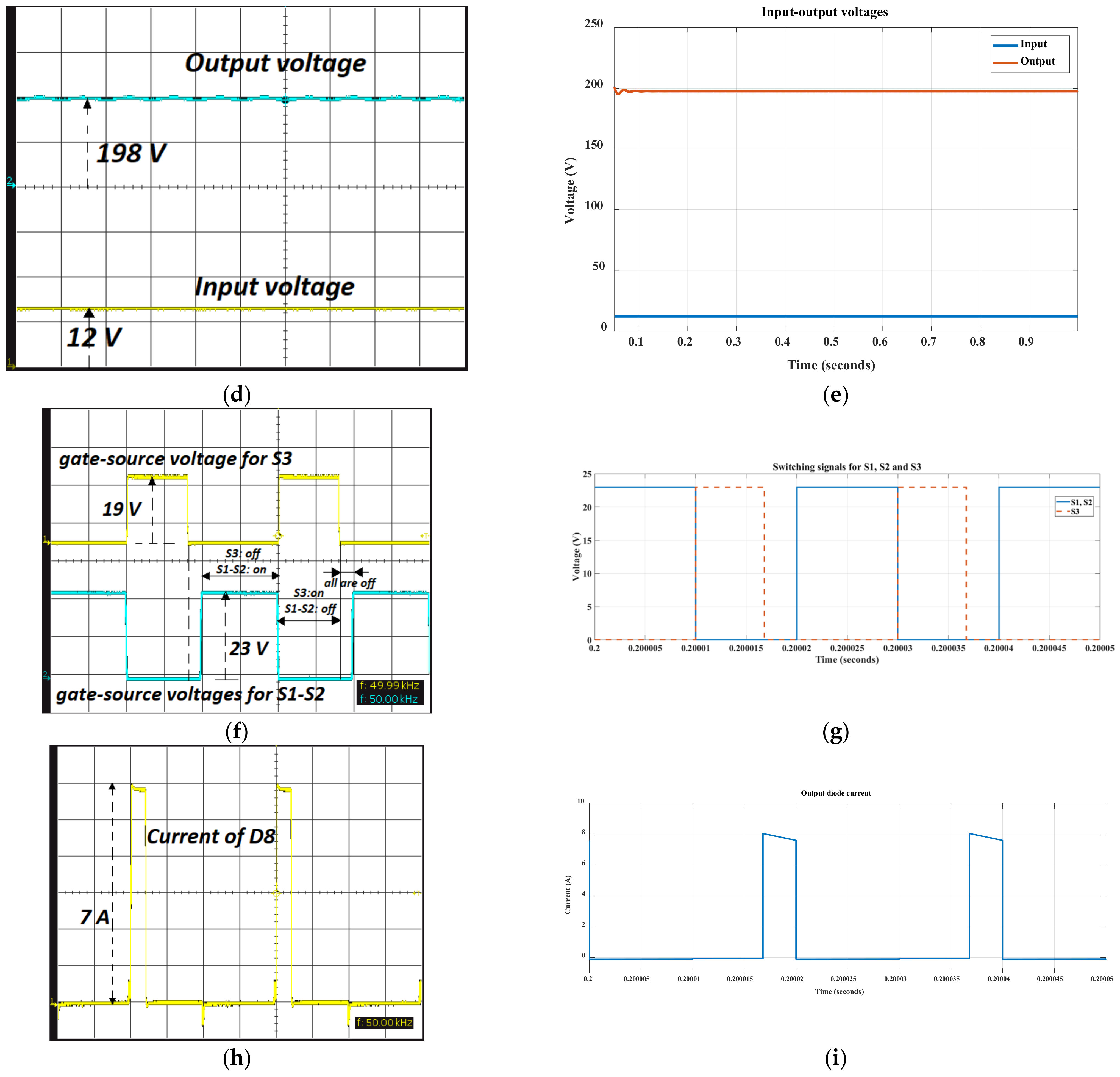
(a) Input-output currents in (b) experiment and (c) simulation; input and output voltages in (d) experiment and (e) simulation; gate-source voltages for the switches in (f) experiment and (g) simulation; and current for the diode D8 in (h) experiment and (i) simulation.
Figure 16b,c present the input and output currents, respectively, for the states where the SC cell does not exist. A current with average values close to 16.66 A is expected at the input source. As can be seen in Figure 16b, the average current of the input source is close to 17 A, and the output current is equal to 1 A. Since the load is a 200 Ω resistance, for 200 V and 200 W, the output current is presented correctly. For 12 V as the input voltage, a voltage close to the 198 VDC across the capacitor C1 is obtained, which has a proper overlap with the expected voltage according to the simulation results. The simulation result is illustrated in Figure 16c to make a comparison with the experimental result. The state of the input and output voltages are shown in Figure 16d,e.
The derived switching voltage waveforms for the power switches S1 to S3 are shown in Figure 16f. The state of the switches can be seen. A switching period is formed by the time durations that the switches S1 and S2 are in on-state and S3 is in off-state; then, the switch S3 is activated, and the switches S1 and S2 are deactivated; and finally, in the third state, all switches are deactivated. All these states are presented for the switches’ states based on the theoretical facts presented in Figure 2, Figure 3 and Figure 4 and Figure 6 and the analysis around the working modes I, II, and III in Section 2. The simulation results for switching PWM signals can be seen in Figure 16g. The current waveform for the output diode D8 is seen in Figure 16h, based on the experimental results, and in Figure 16i, according to simulation results. According to the switching conditions, this diode is activated for a short time duration and in working mode III, when all the switches are in the off-state to charge the capacitor C1.
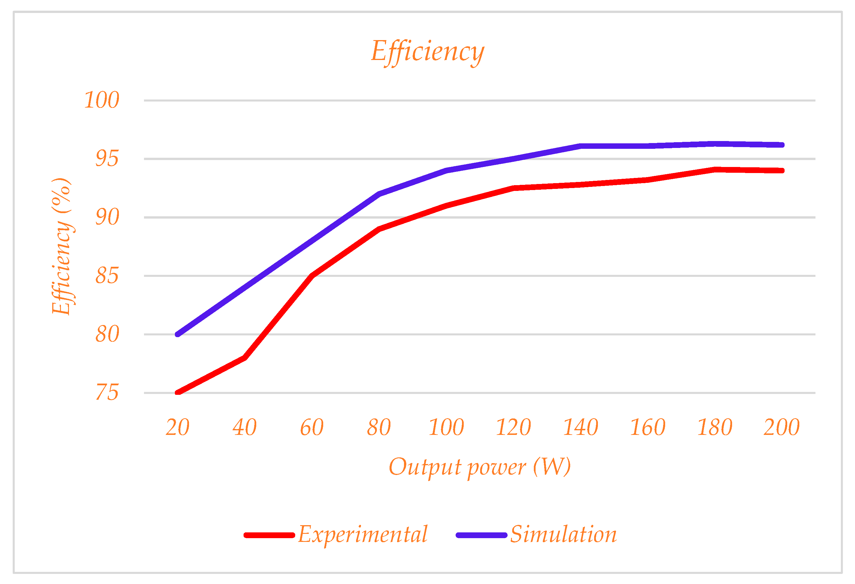
The presented waveforms can experimentally confirm the results of the simulation and the presented theoretical investigations in Section 2. The efficiency of the converter under different load values for powers below 200 W is illustrated in Figure 17. An appropriate overlap can be seen for the implemented and simulation test results. The small differences between the theoretical and experimental results can be interpreted by the parasitic components of the used elements and the working conditions for the laboratory tests or measurement tolerances.
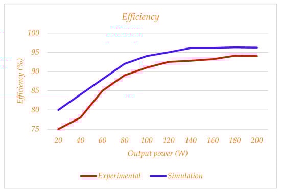
Figure 17.
Efficiency comparison for experimental and simulation under 200 W working conditions.
As mentioned, dynamic and switching losses are the main sources of power losses. Briefly, the dynamic losses are related to the internal resistances of the passive elements and semiconductor devices. The dynamic losses can be decreased by applying fast or ultra-fast semiconductor devices with smaller internal resistances and smaller forward biasing voltages or smaller inductor values. Instead, the switching losses are in connection with the semiconductor devices and their operational conditions in practice. This loss will occur at the switching times and can be obtained simply by multiplying the voltage and current values.
Therefore, it can be found that for the greater switching frequencies, the switching losses are more. In addition, it can be proven that the switching losses are more than the dynamic losses in theory or in practice. Soft switching techniques are normally considered to decrease this type of loss. These techniques are divided into four categories: zero voltage switching (ZVS), zero current switching (ZCS), zero voltage transition (ZVT), and zero current transition (ZCT) techniques. Thanks to these techniques, the total losses of the converter can be decreased.
For the proposed topology with 200 W as the output power, as can be seen in Figure 18, theoretical and experimental power losses of 7.6 W and 12 W are reported. Figure 18a,b present the devices’ power loss values based on the accurate theoretical calculation and measured losses in the laboratory, respectively.
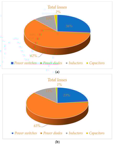
Figure 18.
Total power losses for the devices in (a) theory and (b) practice.
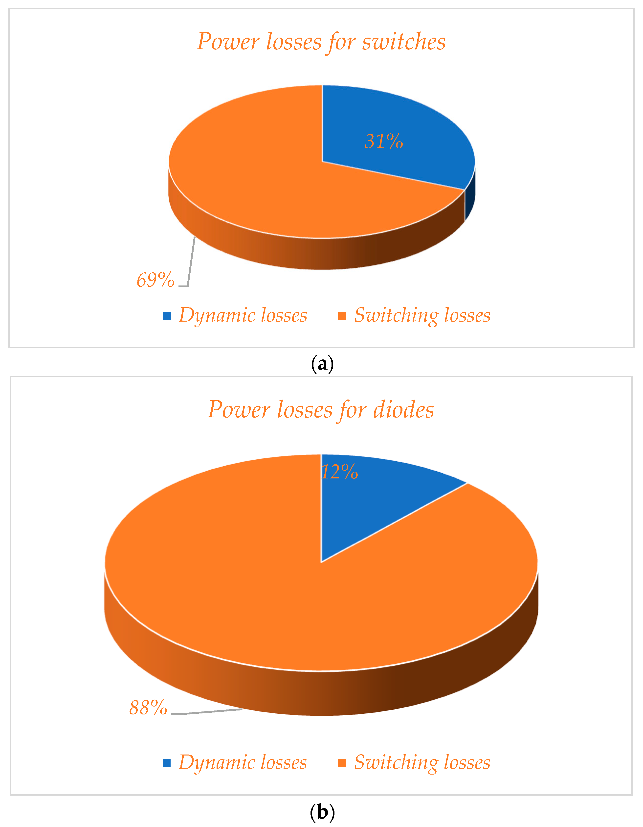
This figure shows that the main source of the power losses is the diodes, and then the switches. The source causing the least loss is the capacitors. In addition, Figure 19 presents the percentage of the dynamic and switching power losses for the switches and diodes. Figure 19a shows the loss distribution for the switches, and Figure 19b presents the losses for the power diodes. According to these figures, 69% of the power losses for the switches are for the switching losses, and 31% are for the dynamic losses. These values are equal to 88% and 12% for the switching and dynamic losses for the diodes, respectively.

Figure 19.
Total power losses for the semiconductor devices’ (a) switches and (b) diodes.
5. Conclusions
A novel double-switched-inductor and single-switched-capacitor-based DC-DC boost converter is presented in this study. The proposed configuration minimizes the input current stresses at the input side thanks to the series and parallel connections of the inductors under switching modes. The proposed SC cell decreases the voltage stresses across the switches and divides the output voltage in half for the switch S3 and the input switches. The switching pattern for the power MOSFETs is easy since two power switches are activated and deactivated simultaneously, and the third switch is in the on-state for the time intervals that the other switches are in off-mode and vice versa. Under any request for higher voltages, the SC-cell can easily double the voltage, and the switches in this block work asynchronously, leading to an easy switching template. The number of elements used in comparison with similar topologies is acceptable considering the gain of the converter. In addition, by using the coupled-inductor configuration, two inductors can be wrapped on a common core, and this directly decreases the weight, cost, and volume of the converter; however, this is not essential and can only be considered for cheaper and lighter configurations.
In addition, by considering the high voltage gain of the converter, the proposed circuit can be applied to grid connections and renewable energy source integrations. Using more SC cells will obtain higher voltage gains. The proposed converter reaches gain up to 68 times higher theoretically for the short duty ratios (D = 0.05–0.15) for switch S3, which is interesting. For a fixed 200 and 400 VDC, an input voltage equal to 24 VDC is used, and these fixed voltages without and with the proposed SC-cell, respectively, are obtained by a simple controller. The voltage stresses across the diodes are limited to a maximum of two times the input voltage (VMax = 48 VDC). Since high-gain applications are the subject of this study, the proposed configuration contains more elements in comparison with the conventional DC-DC converters, which is an issue in terms of the tradeoff between high-gain and high-efficiency applications. In addition, generating the switching signals for three switches is more difficult than for configurations with only one power switch. Wrapping on a common core has some consequences and limitations. Using the standard inductors and testing before their application are advised. To test the correction and reliability of the values of the inductors, for L1 and L2, a single wrapped core, and for L3 and L4, two independent inductors with separate cores are used, as can be seen in Figure 16a. The results show that no serious problem is reported. The tolerance between the inductor’s values is small and ignorable.
Author Contributions
Conceptualization, K.N. and M.M.; methodology, M.M. and E.S.; software, M.M. and E.S.; resources, K.N. and F.M.; data curation, K.N. and F.M.; formal analysis, E.A.; validation, E.A.; writing—original draft preparation, K.N.; writing—review and editing, K.N., M.M. and H.C.; supervision, H.C.; project administration, H.C. All authors have read and agreed to the published version of the manuscript.
Funding
This research received no external funding.
Informed Consent Statement
Not applicable.
Data Availability Statement
The data are available upon reasonable request.
Conflicts of Interest
The authors declare no conflict of interest.
Nomenclature
| RESs | Renewable energy sources |
| PV | Photovoltaic |
| FCs | Fuel cells |
| CCM | Continuous conduction mode |
| DCM | Discontinuous conduction mode |
| BCM | Boundary conduction mode |
| V2G | Vehicle to grid |
| G2V | Grid to vehicle |
| V2V | Vehicle to vehicle |
| PWM | Pulse width modulation |
| ZVS | Zero voltage switching |
| ZCS | Zero current switching |
| CP | Charge pump |
| SL | Switched-inductor |
| SC | Switched-capacitor |
| Inductance of all inductors to | |
| Current for the inductors to | |
| Duty cycle for the switches S1-S2 | |
| Duty cycle for the switch S3 | |
| voltage across the capacitor | |
| Voltage across the drain-source pins of MOSFETs | |
| Voltage across the diodes | |
| Minimum value of the inductors to work at the BCM | |
| Internal resistance of the inductors | |
| Internal resistance of the diodes | |
| Input power | |
| Switching losses | |
| Switching losses of the switches | |
| Switching losses of the diodes | |
| Switching frequency | |
| Parasitic capacitor for the drain-source pins of the switches | |
| Forward voltage for the diodes | |
| Electrical charge across the parasitic capacitor of the diodes |
References
- Lee, H.-S.; Yun, J.-J. High-efficiency bidirectional buck–boost converter for photovoltaic and energy storage systems in a smart grid. IEEE Trans. Power Electron. 2018, 34, 4316–4328. [Google Scholar] [CrossRef]
- Jongudomkarn, J.; Liu, J.; Yanagisawa, Y.; Bevrani, H.; Ise, T. Model predictive control for indirect boost matrix converter based on virtual synchronous generator. IEEE Access 2020, 8, 60364–60381. [Google Scholar] [CrossRef]
- Chen, S.; Zhou, L.; Luo, Q.; Gao, W.; Wei, Y.; Sun, P.; Du, X. Research on topology of the high step-up boost converter with coupled inductor. IEEE Trans. Power Electron. 2019, 34, 10733–10745. [Google Scholar] [CrossRef]
- Janabi, A.; Wang, B. Switched-capacitor voltage boost converter for electric and hybrid electric vehicle drives. IEEE Trans. Power Electron. 2019, 35, 5615–5624. [Google Scholar] [CrossRef]
- Wang, R.; Sun, Q.; Sun, C.; Zhang, H.; Gui, Y.; Wang, P. Vehicle-vehicle energy interaction converter of electric vehicles: A disturbance observer based sliding mode control algorithm. IEEE Trans. Veh. Technol. 2021, 70, 9910–9921. [Google Scholar] [CrossRef]
- George, L.; Gargiulo, G.D.; Lehmann, T.; Hamilton, T.J. A 0.04 mm2 Buck-Boost DC-DC Converter for Biomedical Implants Using Adaptive Gain and Discrete Frequency Scaling Control. IEEE Trans. Biomed. Circuits Syst. 2015, 10, 668–678. [Google Scholar] [CrossRef]
- Bi, K.; Liu, Y.; Zhu, Y.; Fan, Q. An impedance source modular DC/DC converter for energy storage system: Analysis and design. Int. J. Electr. Power Energy Syst. 2021, 133, 107261. [Google Scholar] [CrossRef]
- Srinivasan, M.; Kwasinski, A. Control analysis of parallel DC-DC converters in a DC microgrid with constant power loads. Int. J. Electr. Power Energy Syst. 2020, 122, 106207. [Google Scholar] [CrossRef]
- Apablaza, D.; Muñoz, J. Laboratory implementation of a boost interleaved converter for PV applications. IEEE Lat. Am. Trans. 2016, 14, 2738–2743. [Google Scholar] [CrossRef]
- Das, D.; Madichetty, S.; Singh, B.; Mishra, S. Luenberger observer based current estimated boost converter for PV maximum power extraction—A current sensorless approach. IEEE J. Photovolt. 2018, 9, 278–286. [Google Scholar] [CrossRef]
- Wu, H.; Mu, T.; Ge, H.; Xing, Y. Full-range soft-switching-isolated buck-boost converters with integrated interleaved boost converter and phase-shifted control. IEEE Trans. Power Electron. 2015, 31, 987–999. [Google Scholar] [CrossRef]
- Liu, Q.; Qian, Q.; Ren, B.; Xu, S.; Sun, W.; Yang, L. A Two-Stage Buck–Boost Integrated LLC Converter with Extended ZVS Range and Reduced Conduction Loss for High-Frequency and High-Efficiency Applications. IEEE J. Emerg. Sel. Top. Power Electron. 2019, 9, 727–743. [Google Scholar] [CrossRef]
- Folmer, S.; Stala, R. DC-DC High Voltage Gain Switched Capacitor Converter with Multilevel Output Voltage and Zero-Voltage Switching. IEEE Access 2021, 9, 129692–129705. [Google Scholar] [CrossRef]
- Stala, R.; Chojowski, M.; Waradzyn, Z.; Mondzik, A.; Folmer, S.; Penczek, A.; Skała, A.; Piróg, S. High-gain switched-capacitor DC-DC converter with low count of switches and low voltage stress of switches. IEEE Access 2021, 9, 114267–114281. [Google Scholar] [CrossRef]
- Dashtaki, M.A.; Nafisi, H.; Pouresmaeil, E.; Khorsandi, A. Virtual Inertia Implementation in Dual Two-Level Voltage Source Inverters. In Proceedings of the 2020 IEEE 11th Power Electronics, Drive Systems, and Technologies Conference (PEDSTC), Tehran, Iran, 4–6 February 2020. [Google Scholar]
- Liu, J.; Wang, K.; Zheng, Z.; Li, C.; Li, Y. A dual-active-clamp quasi-resonant isolated boost converter for PV integration to medium-voltage DC grids. IEEE J. Emerg. Sel. Top. Power Electron. 2019, 8, 3444–3456. [Google Scholar] [CrossRef]
- Yang, L.; Yu, W.; Zhang, J. High voltage gain ratio isolated resonant switched-capacitor converter for sustainable energy. IEEE Access 2019, 7, 23055–23067. [Google Scholar] [CrossRef]
- Xue, J.; Lee, H. Enabling high-frequency high-efficiency non-isolated boost converters with quasi-square-wave zero-voltage switching and on-chip dynamic dead-time-controlled synchronous gate drive. IEEE Trans. Power Electron. 2015, 30, 6817–6828. [Google Scholar] [CrossRef]
- Wu, Y.-E.; Ke, Y.-T. A novel bidirectional isolated DC-DC converter with high voltage gain and wide input voltage. IEEE Trans. Power Electron. 2020, 36, 7973–7985. [Google Scholar] [CrossRef]
- Bai, C.; Han, B.; Kwon, B.H.; Kim, M. Highly efficient bidirectional series-resonant DC/DC converter over wide range of battery voltages. IEEE Trans. Power Electron. 2019, 35, 3636–3650. [Google Scholar] [CrossRef]
- Yang, D.; Duan, B.; Zhang, C.; Shang, Y.; Song, J.; Bai, H.; Su, Q. High-Efficiency Bidirectional Three-Level Series-Resonant Converter with Buck-Boost Capacity for High-Output Voltage Applications. IEEE Trans. Transp. Electr. 2021, 7, 969–982. [Google Scholar] [CrossRef]
- Chen, C.; Liu, J.; Lee, H. A 2-MHz 9–45-V input high-efficiency three-switch ZVS step-up/-down hybrid converter. IEEE J. Solid-State Circuits 2020, 56, 855–865. [Google Scholar] [CrossRef]
- Liang, Y.; Liu, X.; Xu, G.; Yue, S. A Dual-Transformer-Based Bidirectional DC–DC Converter of Using Blocking Capacitor for Wide ZVS Range. IEEE Access 2020, 8, 170568–170578. [Google Scholar] [CrossRef]
- Zhang, Y.; Huang, Y.; Fang, P.; Gao, X.; Yang, Y.; Liu, J. Capacitors voltage ripple complementary control on three-level boost fed single-phase VSI with enhanced power decoupling capability. IEEE Trans. Power Electron. 2021, 36, 14220–14236. [Google Scholar] [CrossRef]
- Wu, F.; Wang, K.; Luo, S. Hybrid-Three-Level Current-Fed Series-Resonant Isolated DC-DC Converter and Its Optimization Modulation Strategy. IEEE Trans. Power Electron. 2021, 37, 196–205. [Google Scholar] [CrossRef]
- Wang, Y.; Zhao, C.; Zhang, L. Adaptive High-Power Laser-Based Simultaneous Wireless Information and Power Transfer System with Current-Fed Boost MPPT Converter. IEEE Photon. J. 2021, 13, 8400111. [Google Scholar] [CrossRef]
- Kumar, P.; Veerachary, M. Z-network plus switched-capacitor boost DC–DC converter. IEEE J. Emerg. Sel. Top. Power Electron. 2019, 9, 791–803. [Google Scholar] [CrossRef]
- Panda, K.P.; Bana, P.R.; Kiselychnyk, O.; Wang, J.; Panda, G. A single-source switched-capacitor-based step-up multilevel inverter with reduced components. IEEE Trans. Ind. Appl. 2021, 57, 3801–3811. [Google Scholar] [CrossRef]
- Fardoun, A.A.; Ismail, E.H. Ultra step-up DC–DC converter with reduced switch stress. IEEE Trans. Ind. Appl. 2010, 46, 2025–2034. [Google Scholar] [CrossRef]
- Li, G.; Jin, X.; Chen, X.; Mu, X. A novel quadratic boost converter with low inductor currents. CPSS Trans. Power Electron. Appl. 2020, 5, 1–10. [Google Scholar] [CrossRef]
- Axelrod, B.; Berkovich, Y.; Ioinovici, A. Switched-capacitor/switched-inductor structures for getting transformerless hybrid DC–DC PWM converters. IEEE Trans. Circuits Syst. I Regul. Pap. 2008, 55, 687–696. [Google Scholar] [CrossRef]
- Lakshmi, M.; Hemamalini, S. Nonisolated high gain DC–DC converter for DC microgrids. IEEE Trans. Ind. Electron. 2017, 65, 1205–1212. [Google Scholar] [CrossRef]
- Yang, L.-S.; Liang, T.-J. Analysis and implementation of a novel bidirectional DC–DC converter. IEEE Trans. Ind. Electron. 2011, 59, 422–434. [Google Scholar] [CrossRef]
- Lee, S.-W.; Do, H.-L. Quadratic boost DC–DC converter with high voltage gain and reduced voltage stresses. IEEE Trans. Power Electron. 2018, 34, 2397–2404. [Google Scholar] [CrossRef]
- Pires, V.F.; Cordeiro, A.; Foito, D.; Silva, J.F. High step-up DC–DC converter for fuel cell vehicles based on merged quadratic boost—Ćuk. IEEE Trans. Veh. Technol. 2019, 68, 7521–7530. [Google Scholar] [CrossRef]


Publisher’s Note: MDPI stays neutral with regard to jurisdictional claims in published maps and institutional affiliations. |
© 2022 by the authors. Licensee MDPI, Basel, Switzerland. This article is an open access article distributed under the terms and conditions of the Creative Commons Attribution (CC BY) license (https://creativecommons.org/licenses/by/4.0/).