Abstract
This paper proposes a high-performance control strategy for dc–dc converters supplying combined loads (constant current/power, and/or linear loads). This strategy combines a feedback law with a feedforward compensation. The feedback law is based on full feedback linearization, which guarantees that zero dynamics are avoided. To design a single controller for the three basic converter topologies (i.e., buck, boost and buck–boost), a unified model for these converters is introduced. From the resulting combined control law, the specific control law for each type of converter can be obtained by setting three constant coefficient to 0 or 1. The feedforward compensation is based on the estimated values of the load obtained via a nonlinear observer. The main advantage of this unified approach is that it is implemented by using a single algorithm which can be executed in a dedicated hardware, for instance, a single integrated circuit, providing a unified solution for the control of the mentioned topologies. The good performance of the proposed scheme is verified through simulations and tested via experimental application cases, concluding that this is a good unified solution to control dc–dc converters used in microgrid applications.
1. Introduction
dc–dc converters have been in use for a long time. However, in the last two decades, their applications have increased significantly. For instance, these converters are used for integrating different kinds of power sources to the dc microgrid [1,2]. Other times, they are combined with dc–ac converters for obtaining ac power sources [3,4]. There are many reasons for the increase in the number of applications. Among others, the integration of generation based on renewable energies, transport applications, dc–dc micro and nano-grids and other smart grid applications can be mentioned [5,6,7,8,9]. It is remarkable that the converters in several of these applications feed constant power loads (CPLs) and that the number of these applications is increasing at an enormous rate [10]. However, many times, the same converter must supply other types of loads, such as linear loads and constant current loads (CCLs) and/or a combination of these (i.e., linear loads, CCLs and CPLs).
As mentioned, connection of energy sources and loads through electric power converters is used for building electric power distribution networks. Considering the new paradigm of electric power generation, transmission and distribution, called smart grid [11,12], it is relevant to remark that microgrids are emerging as an important tool to satisfy new standards set for environmental reasons. There are mainly two kinds of microgrids: ac microgrids and dc microgrids [13,14]. dc microgrids are implemented in several applications. Among others, it is possible to use dc microgrids in rural and residential electrification [15,16]. When dc microgrids are designed, dc–dc electronic power converters must be used for adjusting voltage levels between different stages of the dc microgrids. The power flow in microgrids can be controlled by using different control strategies [17,18,19]. The main component to control the power flow in a dc microgrid is the dc–dc electronic power converter [20].
Although there are different types of dc–dc converters, the main three basic topologies are the buck converter (step-down), the boost converter (step-up) and the buck–boost converter (step-down and step-up). From the point of view of the system, these converters present a bilinear state space model when they are loaded with a linear load. However, when they drive CPLs, the bilinear nature of the model is broken because a state variable appears dividing a disturbance input. In such cases, the load introduces a negative incremental resistive effect, causing instability in the system [21,22]. In recent years, many nonlinear control techniques have been applied to obtain high performance when supplying linear loads, CCLs or CPLs, separately. Most of these techniques are inherited from those used for bilinear descriptions. However, with the boom in dc–dc microgrids development [23,24,25], it is increasingly common for dc–dc converters to supply a combination of this type of loads.
In the bilinear models of dc–dc converters, it is well-known that the command signal switches between two values, 0 and 1, which originates switched bilinear networks. A common method to design the command signal is to use an average model [26] to compute a continuous control signal. This signal is then used to modulate the width of a signal pulsating between 0 and 1. Different methods can be found in the literature to design the continuous control signal. Sliding mode control [27,28,29,30,31], passivity-based strategies [32,33,34], predictive control [35,36,37,38,39,40], fuzzy controllers [41] and feedback linearization control (FL) [42] are widely used strategies. FL has been applied in both partial [43,44,45,46] and full mode [47].
An important difference between full FL and the other techniques is the elimination of zero dynamics. Using the average model of the system, full FL is obtained by selecting an output whose relative degree is equal to the order of the system. This output is called a flat output [48], and prevents zero dynamics. On the other techniques, the relative degree of the output is usually less than the order of the system. As a consequence, nonlinear zero dynamics is present in the closed-loop system, and the behavior of this dynamics must be studied in order to guarantee the stability of the closed-loop system.
Although, the three dc–dc converter basic topologies are different, it is possible to design a unified control strategy for all of them, choosing an adequate output to be fed back. The main advantage of a unified approach is that it can be used to design a single integrated circuit (IC) solution that can control any of these converters. To this end, this paper introduces a unique average model for all three converters, and uses a unique flat output for designing a nonlinear controller based on a full FL control strategy. If the load power is considered a disturbance input, and is not included in the design of the feedback controller, this controller will still be able to track load power changes. In this case, the disturbance tracking dynamics will be the same as the reference tracking dynamics. However, it is well-known that disturbance rejection performance can be improved by feedforwarding the load power instantaneous value. Since it is usually not convenient to measure the load power value, it is possible to estimate it using an observer built from the measurements of the state variables [49]. With this in mind, the unified control law proposed in this paper feedforwards estimates of the load power value and its time derivative, improving the transient performance when the load power changes. Additionally, the proposed controller is tested for different types of loads (CPL, CCL and resistive load), and it is found to be stable and have good performance in all cases. Both the proposed controller and observer are easy to tune. A procedure to obtain their feedback gains, based on the desired settling time, is described. Since both the controller and observer apply for the three topologies, after the gains are chosen, it is easy to obtain the control law for each converter. This is done here by setting three coefficients (named , and in this paper) to 0 or 1.
The rest of the paper is organized as follows. Section 2 describes the unified model of the three converters feeding a combined load. Section 3 shows the proposed full FL scheme with feedforward compensation. In Section 4, the load power observer is proposed, and its tuning criterion is described. Section 5 shows the proposed control scheme for the linearized system, and its tuning criterion. Simulation and experimental results that validate the proposal are shown in Section 6 and Section 7, respectively. Finally, in Section 8, conclusions are drawn.
2. Unified Average Model of the Converters
Figure 1 shows the topologies of the synchronous buck, boost and buck–boost converters. For all the converters, E is the input voltage, the output voltage, the inductor current and u the gate signal for the top switch. The combined load is modeled as a resistive load () in parallel with a CPL () (modeled through a current source) and a CCL ().

Figure 1.
Topologies of the synchronous buck, boost and buck–boost converters.
In the continuous conduction mode, the continuous time average models of these converters are merged together into two differential equations using a set of constant coefficients , and :
where is a variable modeling the combined effect of a CPL, a CCL and resistive load:
From Equations (1) and (2), the well-known average models for the buck, boost and buck–boost can be obtained, setting , and , respectively. Here, is the control action, and it is a continuous (derivable) signal that can take any value between 0 and 1. This signal represents the average value, over one switching cycle, of gate signal u of Figure 1. For the purpose of load estimation, it is assumed that can change its value following a ramp profile (constant slope):
3. Proposed Full FL Scheme
A full input–output FL is proposed in this section. By choosing a flat output allows to avoid closed-loop zero dynamics. This implies, for the second-order system (1) and (2), finding an output with relative degree two (the control action only appears after differentiating the output twice with respect to time). The flat output proposed here is
To show that this output is indeed flat, we differentiate this output with respect to time, assuming input voltage E is constant:
It is clear that control action is not present in . Differentiating with respect to time once more, assuming the load power as defined in Equations (3) and (4), the second time derivative of y results in
where
Since is present in Equation (8), we can see that the relative degree of output y is the same as the order of system (1) and (2). Therefore, y is a flat output.
From Equations (5)–(7), it is now possible to define a second-order linear system. The states of this linear system, defined as and , are
Then, the dynamics of and result
where we used Equation (8), and is the input (control action) of the linear system since it contains control action . It is now possible to design a controller for (13) and (14) applying linear control techniques. The output of this linear controller is signal . From , the actual control action , which will be applied to the real system (1) and (2), must be computed. From Equation (8), results in
Table 1 summarizes Equation (15) for the different converter topologies. It can be seen that the results for the buck converter match those shown in [47] when the converter feeds a CPL.

Table 1.
Computation of control action from for the different converter topologies.
4. Combined Load Power Observer
Considering that the combined load power is modeled by Equations (3) and (4), either a reduced-order observer [47] or a full-order observer can be designed. The full-order observer is better when the measured signals are noisy since it provides additional filtering. The compromise is a slightly slower response since the full-order observer has more states. For a given sampling frequency, the effect of the noise on the quality of the observer estimations is more significant as the speed of the observer is increased. After some testing, it was concluded that, for the desired controller and observer speeds and the available hardware, it is better to implement a full-order observer.
To implement the load power observer from the measured signals, first consider the energy in the capacitor:
Differentiating Equation (16) with respect to time and using Equation (2), the energy variation results in
From Equations (3), (4) and (17), the following full-order observer is proposed:
where , and are constant gains that define the dynamics of the observer.
Defining the error signals , and , the observer error dynamics result in
Tuning Criteria
The poles of the observer are the eigenvalues of , and can be placed at any desired locations, as can be seen in computing the characteristic polynomial of . This polynomial is obtained computing the determinant of :
where s is the Laplace transform variable and I is the identity matrix. A criterion for choosing these pole locations is to set two complex conjugate poles using the classical control second-order system and setting the third pole equal to the real part of the other poles (or a multiple of the real part for faster convergence of this pole). This allows to select a damping and a settling time for the response of the observer. Even though the resulting damping will not be the desired one due to the zeros of the system, the settling time will be very close to the desired one [50]. By assuming and , the desired settling time to 1% of the final value, the natural resonance frequency of the second-order system is
Then, the desired closed-loop characteristic polynomial results in
Equating Equation (22) with Equation (24), the gains of the observer result in
where is how many times faster the third pole is than the complex conjugate poles. Using observer (18)–(20), variables and of the linearized system can be computed through Equations (11) and (12), and a linear controller can be implemented. This controller is described in the following section.
5. Proposed Controller for the Linearized System
In this section, a linear controller for systems (13) and (14) is proposed. This controller will be implemented using full state feedback, which allows to place the closed loop poles of the system at any desired locations.
First, the reference signals and must be defined. The control objective is to keep output voltage at a constant reference level . From Equation (11), since is required for both the boost and buck–boost converters, it is clear that a current reference must be found. To find this reference, notice that in steady state , and assuming the references are reached, and . Using these assumptions in Equations (1) and (2), and the fact that the reference is only required for the boost and buck–boost converters, the current reference results in
Now the references for the controller are defined as follows:
To improve the performance in the presence of parametric uncertainties, and achieve zero steady-state error when following a constant reference , an integrator is added to the linear system. Applying full-state feedback, the control action results in
where is the integrator state, with the following differential equation:
By combining Equations (13) and (14) with Equations (31) and (32), the closed-loop system dynamics result in
5.1. Tuning Criteria
The poles of the closed loop controller are the eigenvalues of A, and can be placed at any desired locations, as can be seen by computing the characteristic polynomial of A:
We will use the same criteria as for the observer (a second-order classical control system plus a real pole times the real part of the complex poles). Assuming the damping is , and the desired settling time to 1% of the final value, , is given, the natural resonance frequency of the second-order system is
Then, the desired closed loop characteristic polynomial results in
5.2. Control Loop Summary
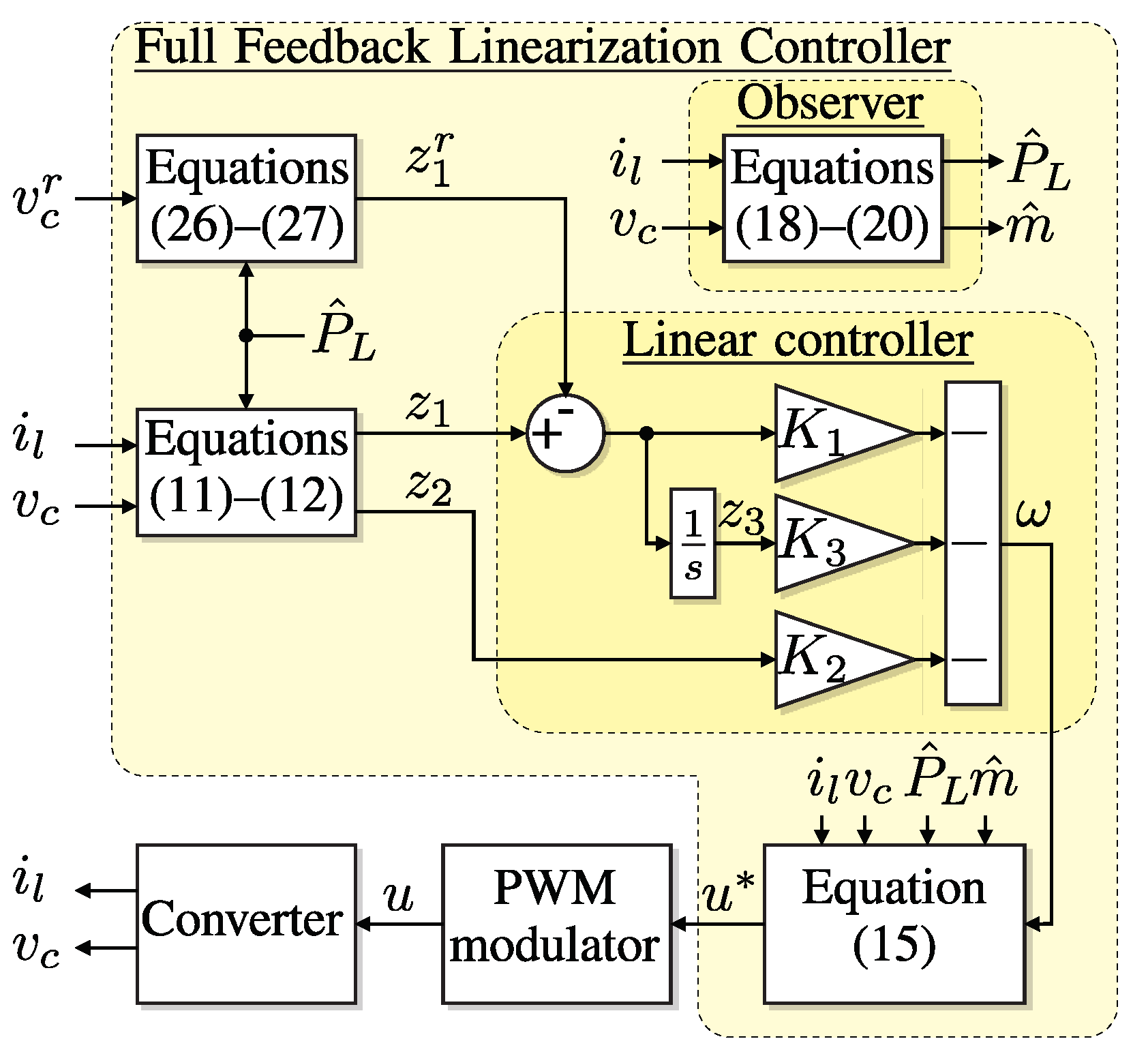
The implementation of the control loop is shown schematically in Figure 2. It can be summarized as follows:
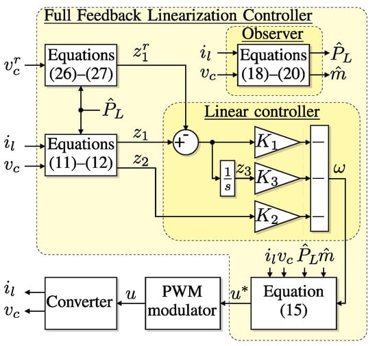
Figure 2.
Controller scheme.
Note that the three different dc–dc topologies can be controlled using the same IC. It is enough to design only one IC, where a three-bit digital word can be input. These bits contain the values of , and set to 0 or 1 depending on the dc–dc topology. The IC complexity is incremented a bit, but it allows to control three different topologies. In addition, it must be noted that the control strategy combines a feedback law based on full input–output FL and a feedforward compensator. This feedforward compensator improves the transient response in presence of load variations.
5.3. Comments about Other Strategies
The control of dc–dc converters has been explored by many researchers and there is an enormous number of works in the literature on this subject. Among others, the cascade double-loop control with voltage and current feedback and variants of this control are proposed in recent works. However, using this control has some drawbacks. On the one hand, in the case of boosting, the feedback of the capacitor voltage causes the transfer function obtained by using Taylor’s linearized technique to have relative degree equal to one. This means that this transfer function presents two poles and a non-minimum phase zero [51]. This zero limits the maximum gain of the external loop since making this gain too large leads to instability. On the other hand, when the converter supplies constant power loads [10,52], the small-signal behavior is such that a positive feedback effect can occur, causing that, for fixed values of the controller parameters, the system becomes unstable in the presence of large and rapid load variations. For this reason, it is not possible to track abruptly changing references and widely varying loads, making these controllers relatively inefficient in applications where large state excursions are necessary.
Mainly for these reasons, several researchers have focused on developing non-linear control strategies to obtain better performance when large excursions of the states occur. Indeed, depending on the output chosen and the way in which the load is treated, the mentioned drawbacks can be mitigated or completely eliminated.
The strategy presented in this paper is especially useful to fully overcome these drawbacks. This is because a full feedback linearization non-linear control strategy with a flat output is implemented. This output presents a relative degree equal to two, matching the system’s order and avoiding the appearance of zero dynamics [53]. Regarding constant power loads, the problem is addressed by introducing a feedforward compensation of the estimated load power. Thus, the strategy presented allows overcoming both drawbacks. In addition, its unified formulation allows the strategy to be applied to any of the basic topologies of dc–dc converters easily.
6. Simulation Results
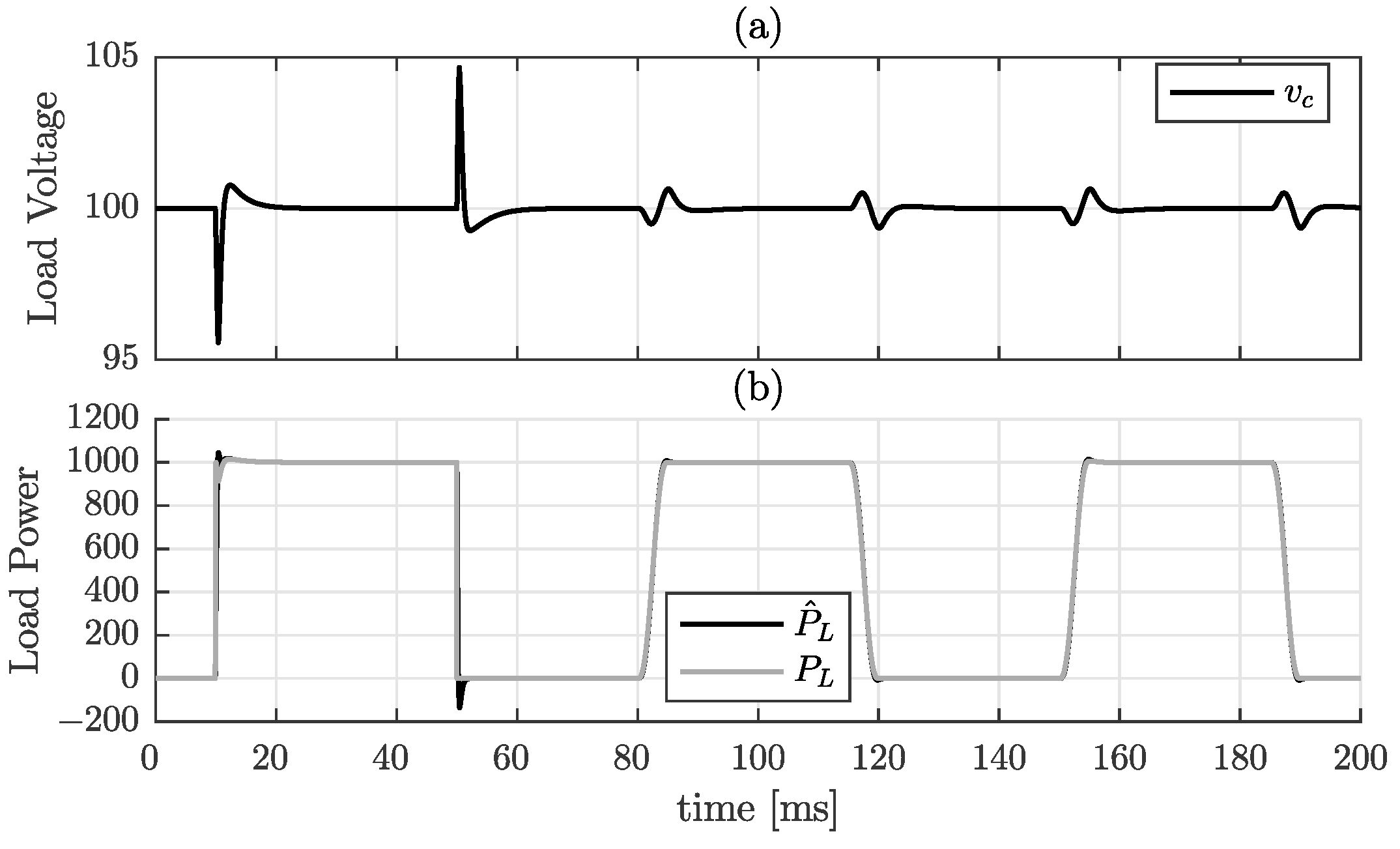
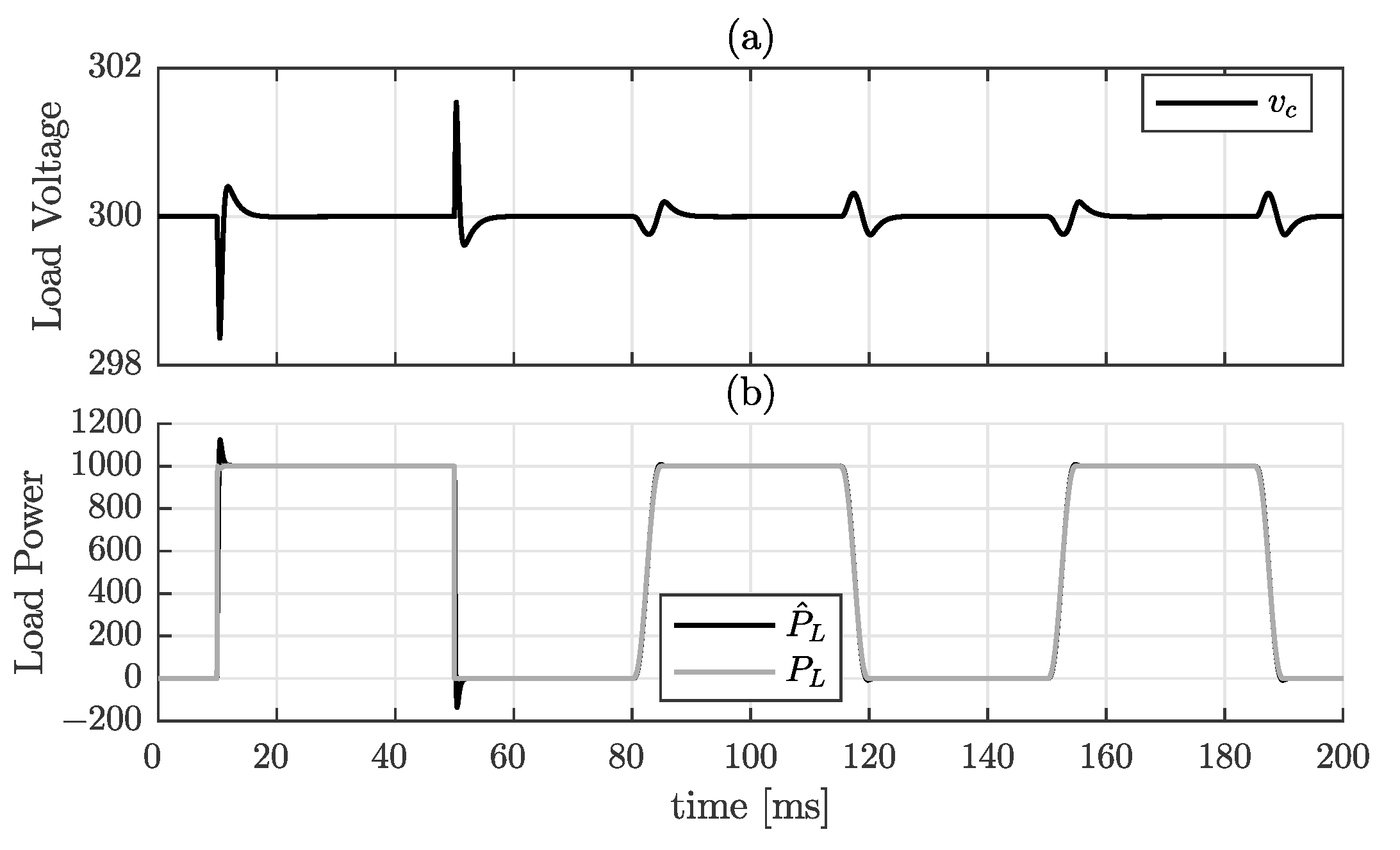
This section shows the simulation results of the proposed control scheme. The three converters were simulated using the parameters described in Table 2. The controller was designed with a settling time ms and [see Equations (37)–(39) for the gain computation], and the observer was designed with ms and [see Equations (25)–(27) for the gain computation]. For the buck converter, the output voltage reference was V, for the boost converter V, and for the buck–boost converter V.

Table 2.
Simulation parameters.
Figure 3 shows the simulation results to load variations for the buck converter, Figure 4 for the boost, and Figure 5 for the buck–boost converter. For these simulations, all converters start in the steady-state with no load. At ms, a resistive load that drains 1 kW is connected and removed at ms. As can be seen in all figures, this load produces the largest dc link voltage transient and observer error, which happens due to the sudden connection/disconnection (step load). At ms, the power of the CPL connected to the dc link is increased from 0 to 1 kW within 5 ms following a soft profile, then, at ms the load is decreased to 0 W following the same profile. As the figures show, the dc link transient and observer error are small for all the converters. Finally, at ms, the CCL connected to the dc link has its current increased so that it takes 1 kW in steady state. This is done within 5 ms following a soft profile, similar to that of the CPL. Then, at ms, the current is decreased to zero, tracking the same profile. In all cases, both the dc link voltage transient and observer error are also small.
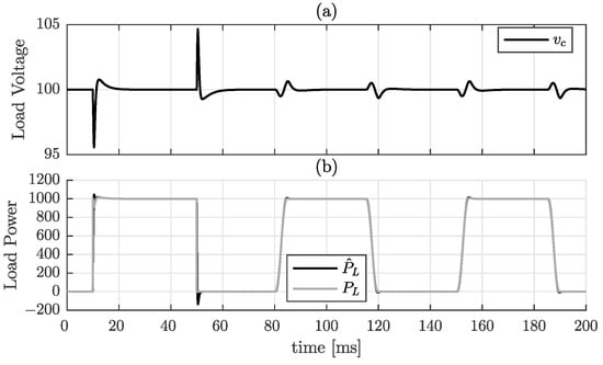
Figure 3.
Simulation results for the buck converter with 1 kW load step changes. (a) dc link voltage. (b) Load power vs. observed load power.
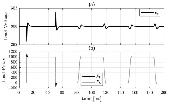
Figure 4.
Simulation results for the boost converter with 1 kW load step changes. (a) dc link voltage. (b) Load power vs. observed load power.
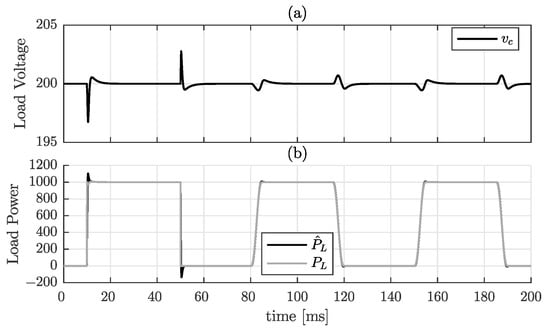
Figure 5.
Simulation results for the buck–boost converter with 1 kW load step changes. (a) dc link voltage. (b) Load power vs. observed load power.
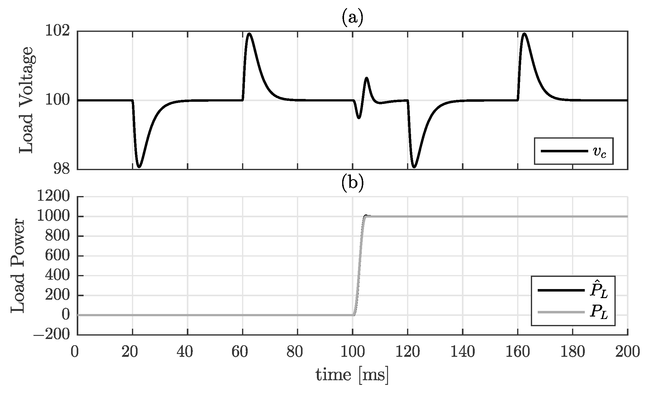
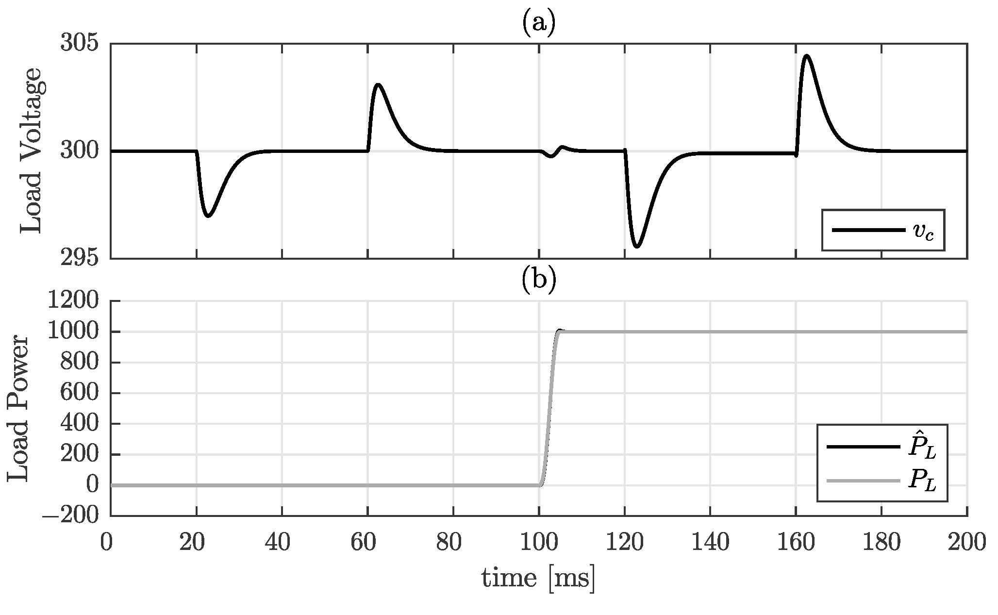
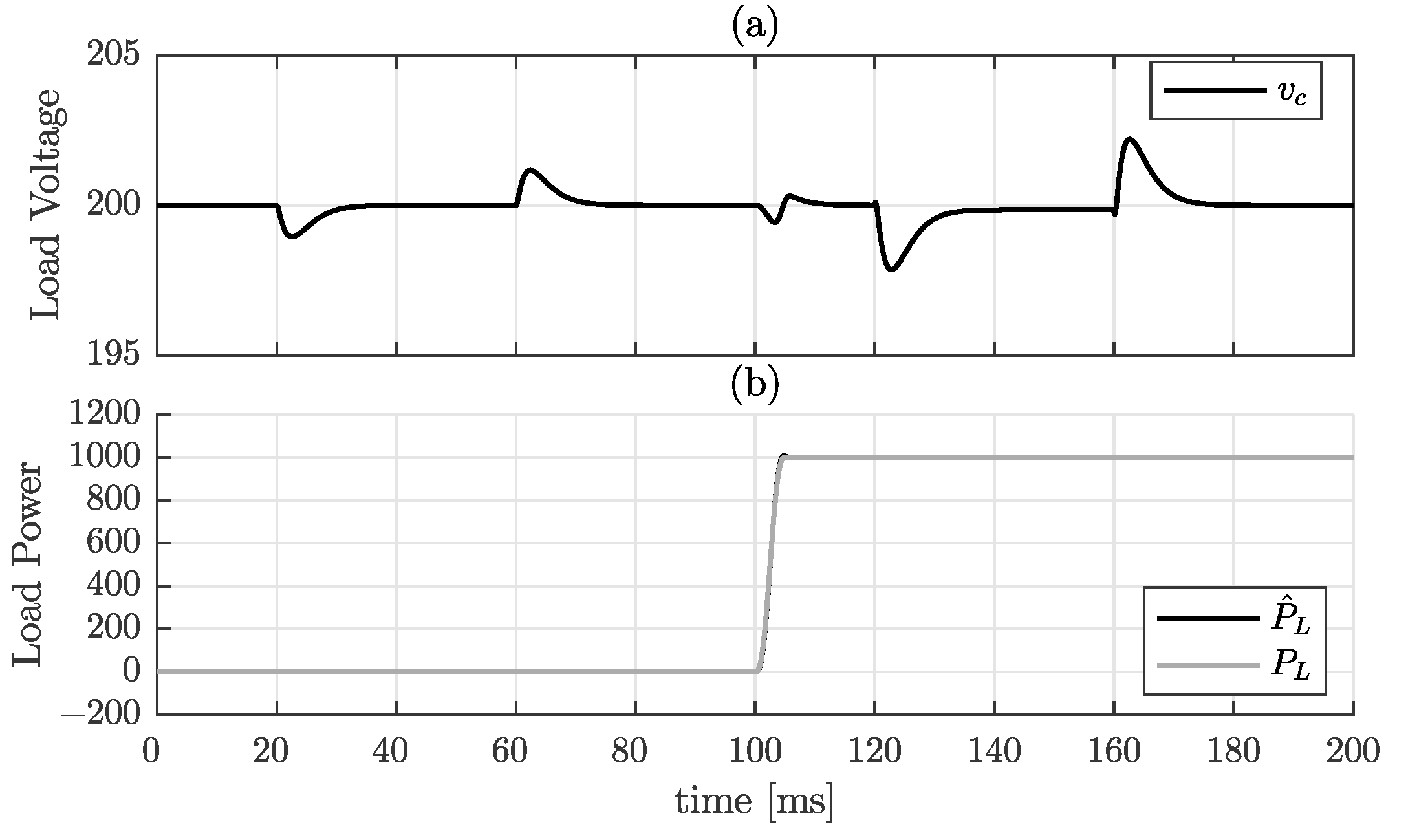
Although the input voltage variation is not considered when modeling the system, Figure 6, Figure 7 and Figure 8 show the simulation results when the input voltage is varied, for the buck, boost and buck–boost converters, respectively. For these simulations, all converters start in steady-state with no load. At ms, the input voltage is increased by and then decreased to its nominal value at ms. Then, at ms, the load is increased to 1 kW (using a CPL). After this, at ms, the input voltage is once again increased by and then decreased to its nominal value at ms. As can be seen in all figures, the effect of this sudden input voltage variation on the output voltage is very small, and is canceled by the controller as a disturbance within the designed settling time. This shows that the proposal is also robust to input voltage variations.
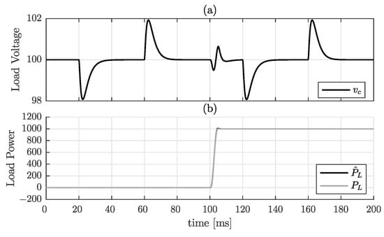
Figure 6.
Simulation results for the buck converter with input voltage changes. (a) dc link voltage. (b) Load power vs. observed load power.
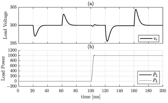
Figure 7.
Simulation results for the boost converter with input voltage changes. (a) dc link voltage. (b) Load power vs. observed load power.

Figure 8.
Simulation results for the buck–boost converter with input voltage changes. (a) dc link voltage. (b) Load power vs. observed load power.
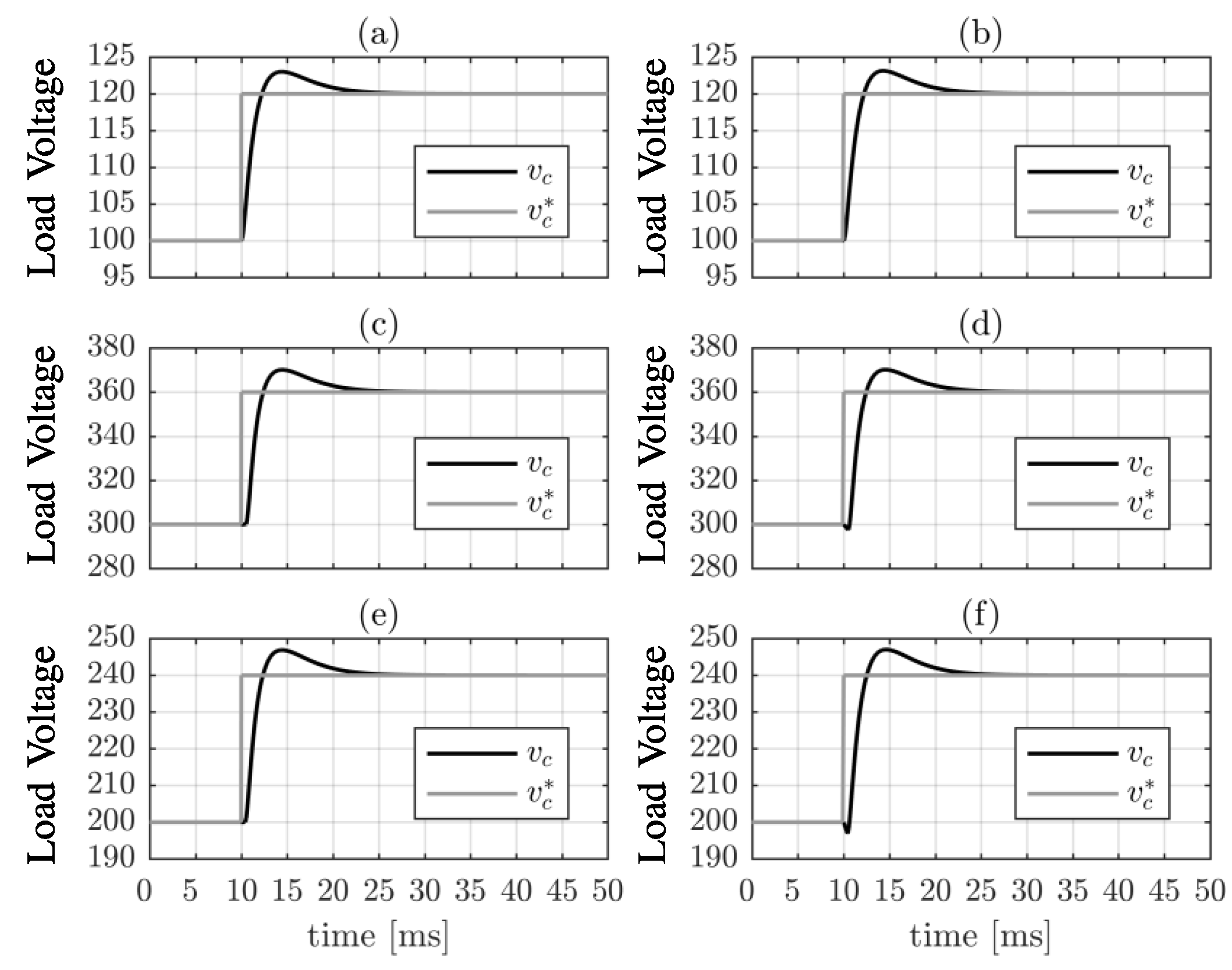
To show the dynamics of the output voltage to voltage reference changes, the previous simulations were repeated for the three converters, with no load and with nominal resistive load. These results are shown in Figure 9. Figure 9a,c,e, show the output voltage of the buck, boost and buck–boost converters, respectively, when the reference voltage is increased 20% from its nominal value, and the converters are operating with no load. As can be seen in these figures, the settling time for all converters is 10 ms, as was expected from the design conditions. Figure 9b,d,f show the same simulations but in these cases, the converters are loaded with a resistive load. In all cases, the resistive load value is selected so that it drains 1 kW after the voltage reference step. As can be seen, the settling time in this case is also 10 ms for all the converters. As can be seen, the responses to reference changes with or without load are very similar. This is expected, as the load is considered as part of the linearization transformation, and the load value is correctly estimated by the observer.
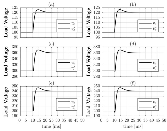
Figure 9.
Simulation results: voltage reference 20% step. (a) Buck with no load. (b) Buck with resistive load. (c) Boost with no load. (d) Boost with resistive load. (e) Buck–boost with no load. (f) Buck–boost with resistive load.
7. Experimental Results: Application Cases
To validate the proposal three application cases are shown in this section.
7.1. Boost Converter with CCL
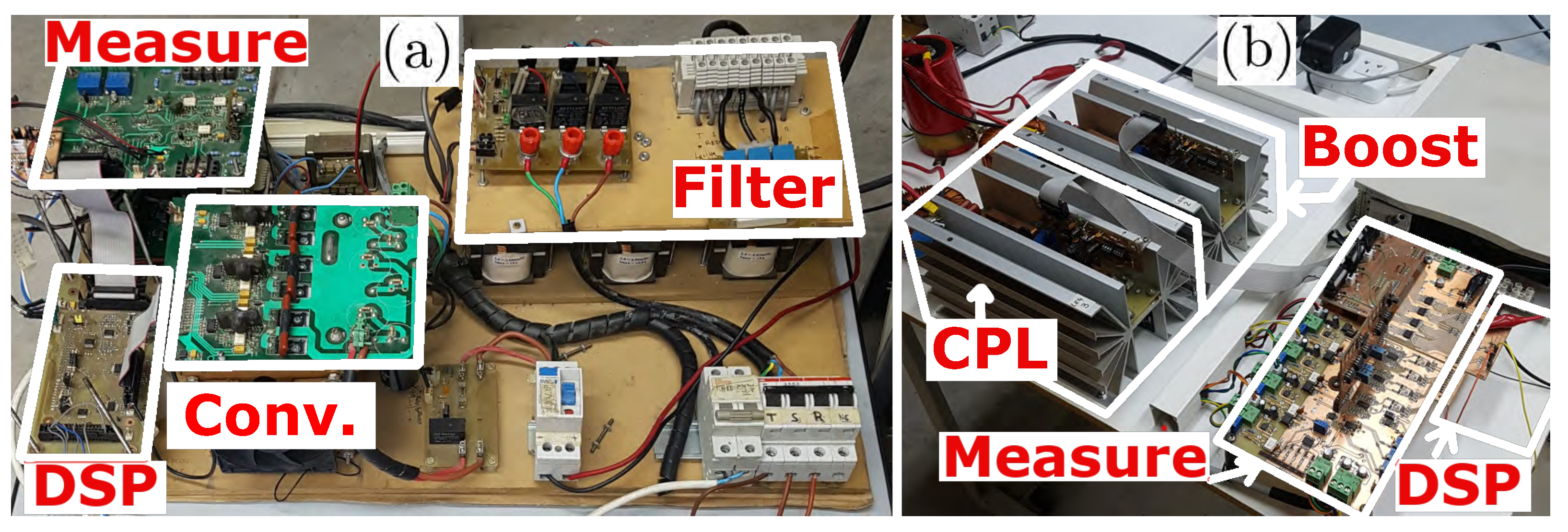
The proposed controller for a boost converter was implemented in a TMS320F28335 DSP, using a sampling time of μs. The converter under test was built using IGBTs IRG4PH50UD, and the inductance and capacitance of this converter were the same as in the simulations ( mH, μF) and so are the parameters of the controller. The switching frequency was 20 kHz, and the output reference was set to V. The input voltage was provided by a 600 V × 25 A power dc voltage source, and was set to V. As CCL a SLH-500-6-1800 AC/DC electronic load was used. A picture of the experimental setup is shown in Figure 10a. Here, only a leg of a three phase converter is used to implement the boost converter (block “Conv.”). The block labeled “measure” is the measurement and level adaptation board, block “DSP” is the interface board connected to the DSP, and block “filter” is the boost inductor. In this configuration, the rated power of the converter is 2 kW.

Figure 10.
Experimental setup. (a) Converter for cases in Section 7.1 and Section 7.3. (b) Converter for case in Section 7.2.
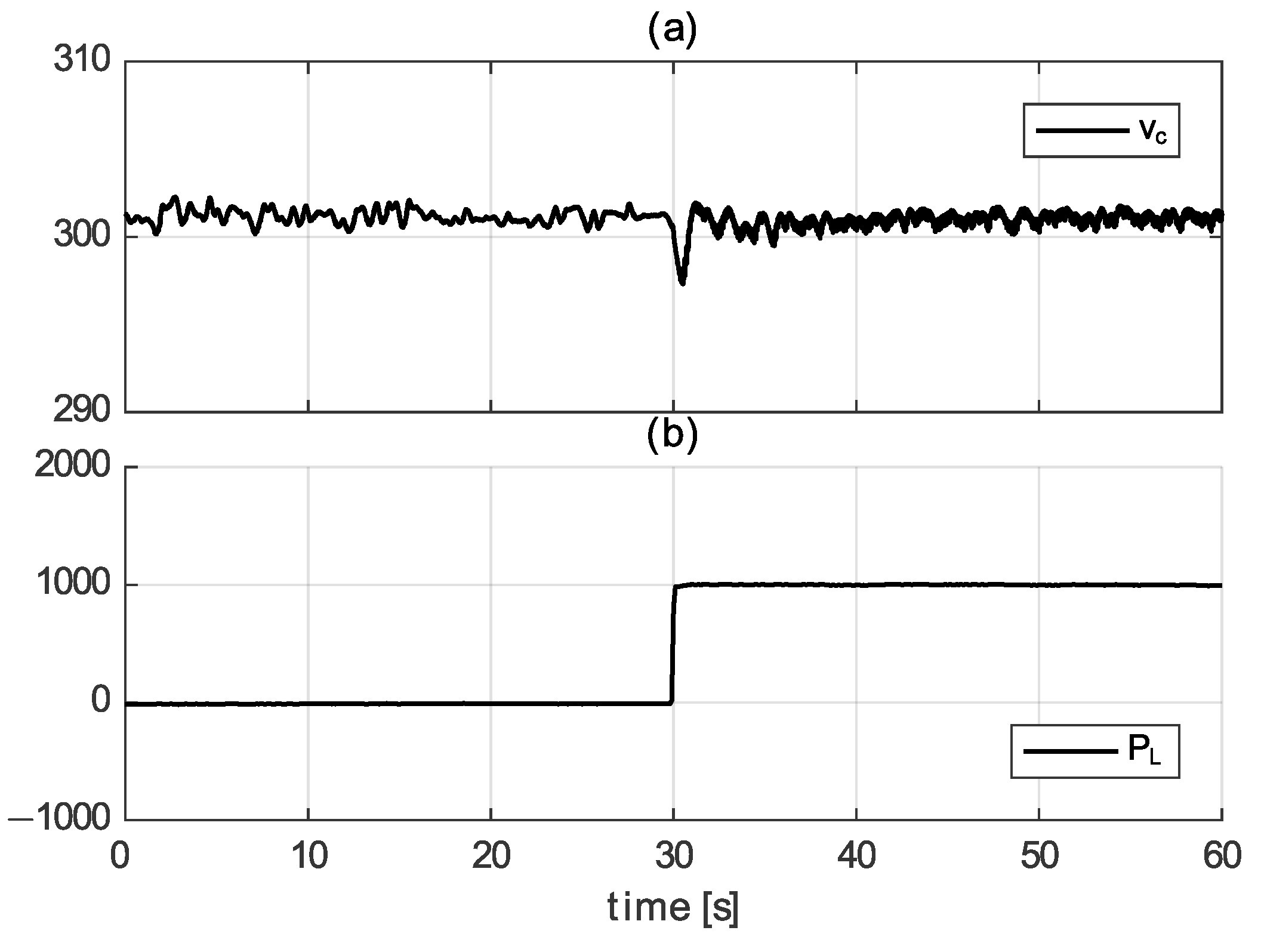
Figure 11a shows output voltage and Figure 11b load power . This load power is obtained by measuring the load current and multiplying it with the measured voltage using the MATH function of the oscilloscope. The experiment starts with the CCL set to zero, and the output voltage at its reference value . At ms, the CCL current is increased to 3.3 A, so it drains 1 kW from the converter. As can be seen, the output voltage converges to its reference value within 2 ms with a transient similar to that in the simulation results.
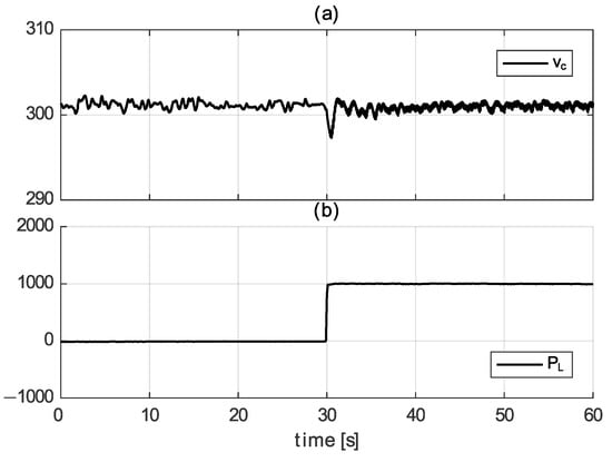
Figure 11.
Experimental results: boost converter feeding a CCL. (a) dc link voltage . (b) Load power .
To show the importance of the feedforward term for improving the performance to load variations, Figure 12 shows the same experimental results as Figure 11, but in this case, the observed power is set to . As can be seen, when the current step is applied to the CCL, the transient is longer (approximately 10 ms) significantly longer than the transient of Figure 11.
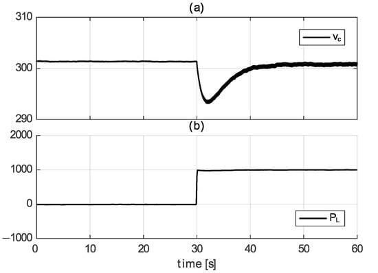
Figure 12.
Experimental results: boost converter feeding a CCL without feedforward. (a) dc link voltage . (b) Load power .
7.2. Boost Converter with Resistive Load and CPL
For another application, the proposed controller for a boost converter was also implemented in a TMS320F28335 DSP, using a sampling time and PWM period of s. This converter uses IRFP4710 Mosfet switches. The parameters of the converter are shown in Table 3. The output voltage reference to V. In this test, a CPL and a resistive load are connected to the output. The CPL is a buck converter built with the same Mosfet switches, feeding a 5.2 Ω resistive load. The resistive load, which is connected at a specified time, is 14.6 Ω. For this application, the controller was designed with a settling time ms and the observer with ms. A picture of the experimental setup is shown in Figure 10b. In this figure the blocks labeled “CPL” and “boost” are identical legs, where one is configured as a boost converter and the other as a buck feeding a resistive load. The block labeled “measure” is the measurement and level adaptation board, block “DSP” is the interface board connected to the DSP. The filters of each converter are toroidal inductors which can be seen behind the heatsinks of each converter. In this configuration, the rated power of the converter is 700 W.

Table 3.
Boost with resistive load and CPL parameters.
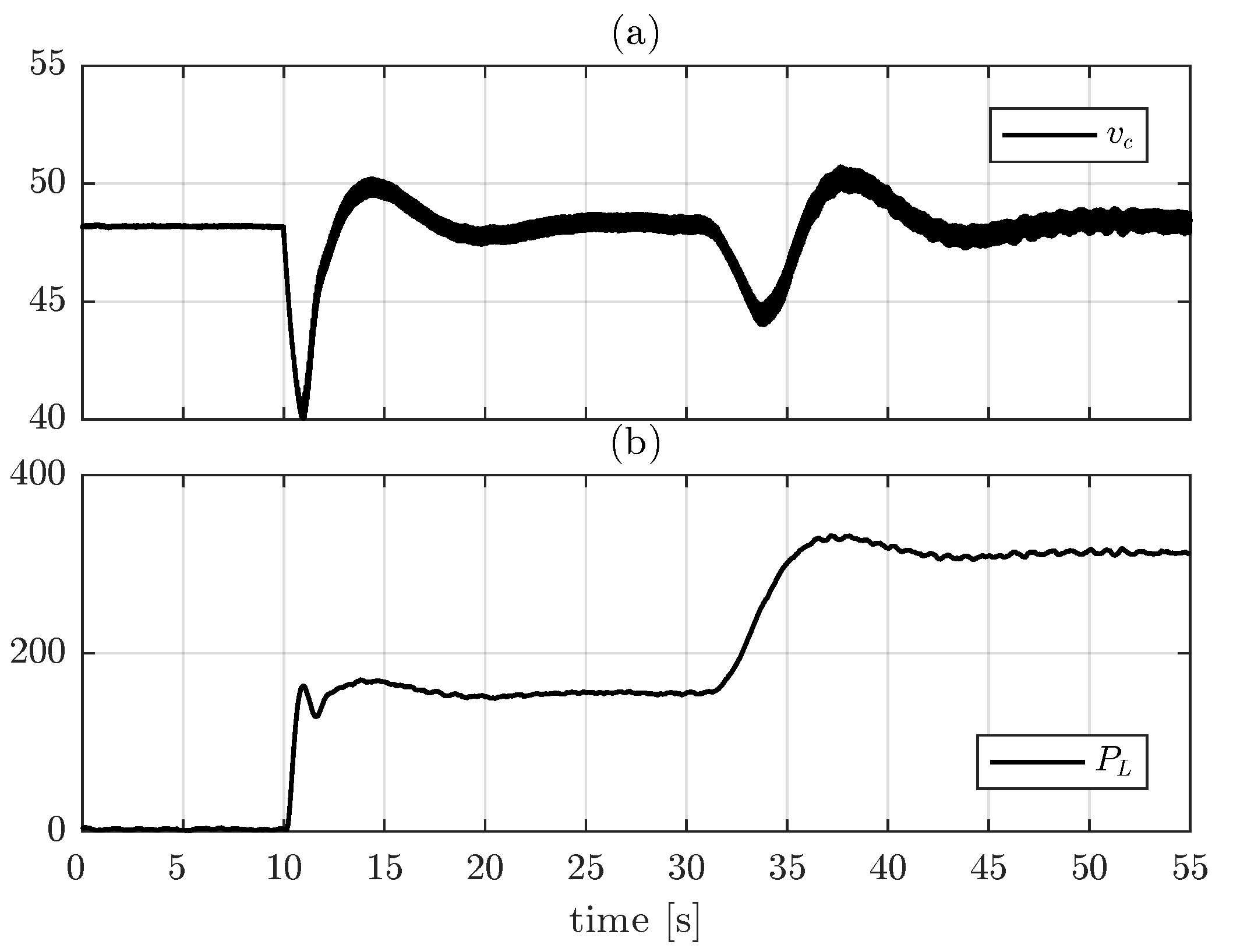
The results of this test are shown in Figure 13. The converter starts with no load and the output voltage at its reference level . At ms, the resistive load is connected to the output, which results in a 10 ms transient, as expected. At approximately ms the CPL power is increased from 0 to 150 W within 5 ms, following a soft profile, which results once again in a 10 ms transient of the output voltage. As shown in these results, the converter behaves as expected.

Figure 13.
Experimental results: boost converter feeding a CPL and a resistive load. (a) dc link voltage . (b) Load power .
7.3. Buck Converter with CCL
For this application, a buck converter was implemented using IRG4PH50UD IGBTs, with the parameters of Table 4. The controller was also implemented in DSP with a sampling time and PWM period of s. The reference voltage was set to V. The converter was loaded with a CCL (the one used in Section 7.1). In this application, the controller was designed with a settling time ms and the observer with ms. A picture of the experimental setup is shown in Figure 10a. In this case, a leg of the three-phase converter is used to implement the buck converter. In this configuration, the rated power of the converter is 1 kW.

Table 4.
Buck with CCL parameters.
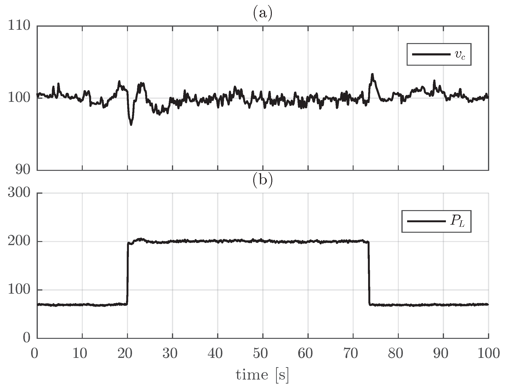
The experimental results are shown in Figure 14. The converter starts with a small load current (draining 67 W), and the output voltage at its reference value . At ms, the load current is increased to 2 A, increasing the load power to 200 W, and at ms, it is decreased to its previous value. As can be seen, the output voltage transients are similar to those seen in the simulation results.
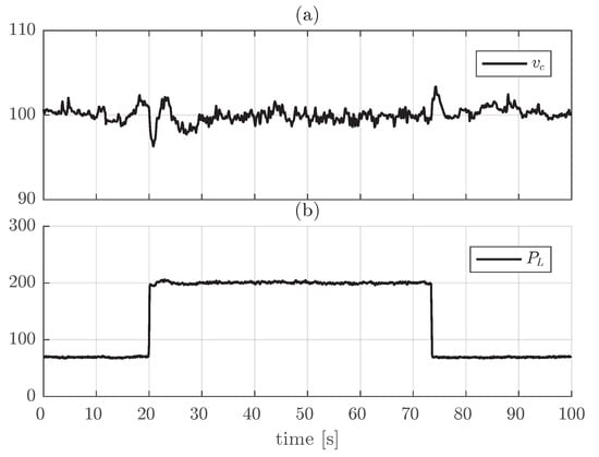
Figure 14.
Experimental results: buck converter feeding a CCL. (a) dc link voltage . (b) Load power .
8. Conclusions
This paper introduces a control strategy to control the output voltage in dc–dc converters supplying combined loads. The proposed strategy combines full FL and feedforward compensation. Full FL is achieved by choosing a flat output, which eliminates zero dynamics. The unified proposal can be used in the three basic dc–dc converter topologies—buck, boost and buck–boost. In order to select the controller for a given topology, it is enough to set the values of three coefficients (, and ) to 0 or 1, in concordance with the type of converter whose output voltage is to be controlled. The proposed controller presents high-performance in the presence of changes in the load value, even for combined linear and nonlinear loads. The proposal was validated through the use of both simulation and experimental results. This algorithm, based on full feedback linearization, is a unified solution for the control of three of the most popular dc–dc converters used in microgrid applications, and can be implemented in a single integrated circuit, allowing a convenient solution for the control of these converters.
Author Contributions
Conceptualization, J.A.S., S.G.J. and C.A.B.; software S.G.J.; validation, S.G.J.; writing—original draft preparation J.A.S. and S.G.J.; writing—review and editing, C.A.B. All authors have read and agreed to the published version of the manuscript.
Funding
This research was funded by Consejo Nacional de Investigaciones Científicas y Técnicas (CONICET) and Universidad Nacional del Sur (UNS), Argentina.
Institutional Review Board Statement
Not applicable.
Informed Consent Statement
Not applicable.
Data Availability Statement
Not applicable.
Conflicts of Interest
The authors declare no conflict of interest.
References
- Abbasi, M.; Abbasi, E.; Li, L.; Tousi, B. Design and analysis of a high-gain step-up/down modular DC–DC converter with continuous input current and decreased voltage stress on power switches and switched-capacitors. Sustainability 2021, 13, 5243. [Google Scholar] [CrossRef]
- Worku, M.Y. Recent Advances in Energy Storage Systems for Renewable Source Grid Integration: A Comprehensive Review. Sustainability 2022, 14, 5985. [Google Scholar] [CrossRef]
- Khan, M.Y.A.; Liu, H.; Habib, S.; Khan, D.; Yuan, X. Design and performance evaluation of a step-up DC–DC converter with dual loop controllers for two stages grid connected PV inverter. Sustainability 2022, 14, 811. [Google Scholar] [CrossRef]
- Jorge, S.G.; Solsona, J.A.; Busada, C.A. Nonlinear Control of a Two-Stage Single-Phase DC–AC Converter. IEEE J. Emerg. Sel. Top. Ind. Electron. 2022, 3, 1038–1045. [Google Scholar] [CrossRef]
- Hossain, E.; Perez, R.; Nasiri, A.; Bayindir, R. Stability improvement of microgrids in the presence of constant power loads. Int. J. Electr. Power Energy Syst. 2018, 96, 442–456. [Google Scholar] [CrossRef]
- Lenz, E.; Pagano, D.J.; Stramosk, V. Nonlinear control applied to a dc-dc power converter and the load sharing problem in a dc microgrid. IFAC Proc. Vol. 2014, 47, 534–539. [Google Scholar] [CrossRef]
- Behera, R.; Parida, S. DC microgrid management using power electronics converters. In Proceedings of the 2014 Eighteenth National Power Systems Conference (NPSC), Guwahati, India, 18–20 December 2014; pp. 1–6. [Google Scholar]
- Herrera, L.; Zhang, W.; Wang, J. Stability Analysis and Controller Design of DC Microgrids With Constant Power Loads. IEEE Trans. Smart Grid 2017, 8, 881–888. [Google Scholar]
- Schmidt, S.; Richter, M.; Oberrath, J.; Mercorelli, P. Control oriented modeling of DC-DC converters. IFAC-PapersOnLine 2018, 51, 331–336. [Google Scholar]
- Hossain, E.; Perez, R.; Nasiri, A.; Padmanaban, S. A comprehensive review on constant power loads compensation techniques. IEEE Access 2018, 6, 33285–33305. [Google Scholar] [CrossRef]
- Cabana-Jiménez, K.; Candelo-Becerra, J.E.; Sousa Santos, V. Comprehensive analysis of microgrids configurations and topologies. Sustainability 2022, 14, 1056. [Google Scholar] [CrossRef]
- Souza Junior, M.E.T.; Freitas, L.C.G. Power Electronics for Modern Sustainable Power Systems: Distributed Generation, Microgrids and Smart Grids-A Review. Sustainability 2022, 14, 3597. [Google Scholar] [CrossRef]
- Zolfaghari, M.; Gharehpetian, G.B.; Shafie-khah, M.; Catalão, J.P. Comprehensive review on the strategies for controlling the interconnection of AC and DC microgrids. Int. J. Electr. Power Energy Syst. 2022, 136, 107742. [Google Scholar] [CrossRef]
- ShahidUllah; Haidar, A.M.; Hoole, P.; Zen, H.; Ahfock, T. The current state of Distributed Renewable Generation, challenges of interconnection and opportunities for energy conversion based DC microgrids. J. Clean. Prod. 2020, 273, 122777. [Google Scholar] [CrossRef]
- Nasir, M.; Iqbal, S.; Khan, H.A.; Vasquez, J.C.; Guerrero, J.M. Sustainable rural electrification through solar PV DC microgrids-An architecture-based assessment. Processes 2020, 8, 1417. [Google Scholar] [CrossRef]
- Ali, S.; Zheng, Z.; Aillerie, M.; Sawicki, J.P.; Pera, M.C.; Hissel, D. A review of DC Microgrid energy management systems dedicated to residential applications. Energies 2021, 14, 4308. [Google Scholar] [CrossRef]
- Erenturk, K.; Draou, A.; AlKassem, A. Design and Comparison of Different Types of Synergetic Controllers for Islanded DC Microgrids. Sustainability 2022, 14, 8792. [Google Scholar] [CrossRef]
- Muñoz, C.; Rivera, M.; Villalón, A.; Baier, C.R.; Muñoz, J.; Ramirez, R.O.; Wheeler, P. Predictive Control with Current-Based Maximum Power Point-Tracking for On-Grid Photovoltaic Applications. Sustainability 2021, 13, 3037. [Google Scholar] [CrossRef]
- Azar, A.T.; Abed, A.M.; Abdulmajeed, F.A.; Hameed, I.A.; Kamal, N.A.; Jawad, A.J.M.; Abbas, A.H.; Rashed, Z.A.; Hashim, Z.S.; Sahib, M.A.; et al. A New Nonlinear Controller for the Maximum Power Point Tracking of Photovoltaic Systems in Micro Grid Applications Based on Modified Anti-Disturbance Compensation. Sustainability 2022, 14, 10511. [Google Scholar] [CrossRef]
- Francés, A.; Asensi, R.; García, O.; Prieto, R.; Uceda, J. Modeling Electronic Power Converters in Smart DC Microgrids-An Overview. IEEE Trans. Smart Grid. 2018, 9, 6274–6287. [Google Scholar] [CrossRef]
- Mosskull, H. Constant power load stabilization. Control Eng. Pract. 2018, 72, 114–124. [Google Scholar] [CrossRef]
- Mayo-Maldonado, J.; Ruiz-Martinez, O.; Escobar, G.; Maupong, T.; Valdez-Resendiz, J.; Rosas-Caro, J. Power shaping control of DC–DC converters with constant power loads. Control Eng. Pract. 2020, 105, 104639. [Google Scholar] [CrossRef]
- Negri, S.; Tironi, E.; Superti-Furga, G.; Ubezio, G. Control and fault analysis of multiport converters for low voltage DC distribution systems. Int. J. Electr. Power Energy Syst. 2013, 124, 106335. [Google Scholar] [CrossRef]
- Srinivasan, M.; Kwasinski, A. Control analysis of parallel DC-DC converters in a DC microgrid with constant power loads. Int. J. Electr. Power Energy Syst. 2020, 122, 106207. [Google Scholar] [CrossRef]
- Rani, P.H.; Navasree, S.; George, S.; Ashok, S. Fuzzy logic supervisory controller for multi-input non-isolated DC to DC converter connected to DC grid. Int. J. Electr. Power Energy Syst. 2019, 112, 49–60. [Google Scholar] [CrossRef]
- Pavlovic, T.; Bjazic, T.; Ban, Z. Simplified averaged models of DC–DC power converters suitable for controller design and microgrid simulation. IEEE Trans. Power Electron. 2013, 28, 3266–3275. [Google Scholar] [CrossRef]
- Utkin, V. Sliding mode control of DC/DC converters. J. Frankl. Inst. 2013, 350, 2146–2165. [Google Scholar] [CrossRef]
- Tan, S.C.; Lai, Y.M.; Tse, C.K. A unified approach to the design of PWM-based sliding-mode voltage controllers for basic DC-DC converters in continuous conduction mode. IEEE Trans. Circuits Syst. I Regul. Pap. 2006, 53, 1816–1827. [Google Scholar]
- Pandey, S.K.; Patil, S.L.; Ginoya, D.; Chaskar, U.M.; Phadke, S.B. Robust control of mismatched buck dc–dc converters by pwm-based sliding mode control schemes. Control Eng. Pract. 2019, 84, 183–193. [Google Scholar] [CrossRef]
- Tian, Z.; Lyu, Z.; Yuan, J.; Wang, C. UDE-based sliding mode control of DC–DC power converters with uncertainties. Control Eng. Pract. 2019, 83, 116–128. [Google Scholar] [CrossRef]
- Sferlazza, A.; Albea-Sanchez, C.; Martínez-Salamero, L.; Garcia, G.; Alonso, C. Min-Type Control Strategy of a DC–DC Synchronous Boost Converter. IEEE Trans. Ind. Electron. 2020, 67, 3167–3179. [Google Scholar] [CrossRef]
- Hassan, M.A.; Li, E.P.; Li, X.; Li, T.; Duan, C.; Chi, S. Adaptive Passivity-Based Control of DC-DC Buck Power Converter with Constant Power Load in DC Microgrid Systems. IEEE J. Emerg. Sel. Top. Power Electron. 2018, 7, 2029–2040. [Google Scholar] [CrossRef]
- He, W.; Soriano-Rangel, C.A.; Ortega, R.; Astolfi, A.; Mancilla-David, F.; Li, S. Energy shaping control for buck–boost converters with unknown constant power load. Control Eng. Pract. 2018, 74, 33–43. [Google Scholar] [CrossRef]
- He, W.; Ortega, R.; Machado, J.E.; Li, S. An Adaptive Passivity-Based Controller of a Buck-Boost Converter with a Constant Power Load. Asian J. Control 2017, 21, 581–595. [Google Scholar] [CrossRef]
- Geyer, T.; Papafotiou, G.; Morari, M. Hybrid model predictive control of the step-down DC–DC converter. IEEE Trans. Control Syst. Technol. 2008, 16, 1112–1124. [Google Scholar] [CrossRef]
- Xie, Y.; Ghaemi, R.; Sun, J.; Freudenberg, J.S. Model predictive control for a full bridge DC/DC converter. IEEE Trans. Control Syst. Technol. 2011, 20, 164–172. [Google Scholar]
- Karamanakos, P.; Geyer, T.; Manias, S. Direct voltage control of DC–DC boost converters using enumeration-based model predictive control. IEEE Trans. Power Electron. 2013, 29, 968–978. [Google Scholar] [CrossRef]
- Dehghanzadeh, A.; Farahani, G.; Vahedi, H.; Al-Haddad, K. Model predictive control design for DC-DC converters applied to a photovoltaic system. Int. J. Electr. Power Energy Syst. 2018, 103, 537–544. [Google Scholar] [CrossRef]
- Hausberger, T.; Kugi, A.; Eder, A.; Kemmetmüller, W. High-speed nonlinear model predictive control of an interleaved switching DC/DC-converter. Control Eng. Pract. 2020, 103, 104576. [Google Scholar] [CrossRef]
- Andres-Martinez, O.; Flores-Tlacuahuac, A.; Ruiz-Martinez, O.; Mayo-Maldonado, J. Nonlinear Model Predictive Stabilization of DC-DC Boost Converters with Constant Power Loads. IEEE J. Emerg. Sel. Top. Power Electron. 2020, 9, 822–830. [Google Scholar] [CrossRef]
- Babes, B.; Hamouda, N.; Albalawi, F.; Aissa, O.; Ghoneim, S.S.; Abdelwahab, S.A.M. Experimental Investigation of an Adaptive Fuzzy-Neural Fast Terminal Synergetic Controller for Buck DC/DC Converters. Sustainability 2022, 14, 7967. [Google Scholar] [CrossRef]
- Sira-Ramirez, H.; Ilic-Spong, M. Exact linearization in switched-mode DC-to-DC power converters. Int. J. Control 1989, 50, 511–524. [Google Scholar] [CrossRef]
- Roshan, Y.M.; Moallem, M. Control of nonminimum phase load current in a boost converter using output redefinition. IEEE Trans. Power Electron. 2014, 29, 5054–5062. [Google Scholar] [CrossRef]
- Arora, S.; Balsara, P.; Bhatia, D. Input–Output Linearization of a Boost Converter With Mixed Load (Constant Voltage Load and Constant Power Load). IEEE Trans. Power Electron. 2019, 34, 815–825. [Google Scholar] [CrossRef]
- Martinez-Treviño, B.A.; El Aroudi, A.; Cid-Pastor, A.; Martinez-Salamero, L. Nonlinear Control for Output Voltage Regulation of a Boost Converter With a Constant Power Load. IEEE Trans. Power Electron. 2019, 34, 10381–10385. [Google Scholar] [CrossRef]
- Bhattacharyya, D.; Padhee, S.; Pati, K.C. Modeling of DC–DC converter using exact feedback linearization method: A discussion. IETE J. Res. 2019, 65, 843–854. [Google Scholar] [CrossRef]
- Solsona, J.A.; Jorge, S.G.; Busada, C.A. Nonlinear Control of a Buck Converter Which Feeds a Constant Power Load. IEEE Trans. Power Electron. 2015, 30, 7193–7201. [Google Scholar] [CrossRef]
- Gensior, A.; Woywode, O.; Rudolph, J.; Guldner, H. On differential flatness, trajectory planning, observers, and stabilization for DC–DC converters. IEEE Trans. Circuits Syst. I Regul. Pap. 2006, 53, 2000–2010. [Google Scholar] [CrossRef]
- Cimini, G.; Ippoliti, G.; Orlando, G.; Longhi, S.; Miceli, R. A unified observer for robust sensorless control of DC–DC converters. Control Eng. Pract. 2017, 61, 21–27. [Google Scholar] [CrossRef]
- Franklin, G.F.; Powell, J.D.; Emami-Naeini, A. Feedback Control of Dynamic Systems; Addison-Wesley Longman Publishing Co., Inc.: Boston, MA, USA, 1993. [Google Scholar]
- Kobaku, T.; Patwardhan, S.C.; Agarwal, V. Experimental evaluation of internal model control scheme on a DC–DC boost converter exhibiting nonminimum phase behavior. IEEE Trans. Power Electron. 2017, 32, 8880–8891. [Google Scholar] [CrossRef]
- Ahmad, S.; Ali, A. Active disturbance rejection control of DC–DC boost converter: A review with modifications for improved performance. IET Power Electron. 2019, 12, 2095–2107. [Google Scholar] [CrossRef]
- Isidori, A. The zero dynamics of a nonlinear system: From the origin to the latest progresses of a long successful story. Eur. Control 2013, 19, 369–378. [Google Scholar] [CrossRef]
Publisher’s Note: MDPI stays neutral with regard to jurisdictional claims in published maps and institutional affiliations. |
© 2022 by the authors. Licensee MDPI, Basel, Switzerland. This article is an open access article distributed under the terms and conditions of the Creative Commons Attribution (CC BY) license (https://creativecommons.org/licenses/by/4.0/).


