Abstract
The market for photovoltaic modules is expanding rapidly, with more than 500 GW installed capacity. Consequently, there is an urgent need to prepare for the comprehensive recycling of end-of-life solar modules. Crystalline silicon remains the primary photovoltaic technology, with CdTe and CIGS taking up much of the remaining market. Modules can be separated by crushing or cutting, or by thermal or solvent-based delamination. Separation and extraction of semiconductor materials can be achieved through manual, mechanical, wet or dry chemical means, or a combination. Crystalline silicon modules are currently recycled through crushing and mechanical separation, but procedures do exist for extraction and processing of intact wafers or wafer pieces. Use of these processes could lead to the recovery of higher grades of silicon. CdTe panels are mostly recycled using a chemical leaching process, with the metals recovered from the leachate. CIGS can be recycled through oxidative removal of selenium and thermochemical recovery of the metals, or by electrochemical or hydrometallurgical means. A remaining area of concern is recycling of the polymeric encapsulant and backsheet materials. There is a move away from the use of fluorinated backsheet polymers which may allow for improved recycling, but further research is required to identify materials which can be recycled readily whilst also being able to withstand outdoor environments for multi-decadal timespans.
1. Introduction
Solar photovoltaic (PV) technology is widely recognised as key to realising fully decarbonised energy generation, and as such is a vital tool in combatting climate change [1,2]. As the importance and impact of climate change have become increasingly recognised globally, the rate of uptake and installation of PV modules has increased almost exponentially, from approximately 1.4 gigawatts total globally installed capacity in 2000 to more than 500 gigawatts in 2018 [2,3,4,5]. Although some greenhouse gas emissions are typically involved during the production process, PV modules do not produce greenhouse gas emissions during use, thereby resulting in a minimal environmental impact for each unit of electricity generated [1,4,6]. PV modules are typically rated as having a projected lifespan of 25 years [4,5,7]. Consequently, the significant increase in PV module production over the last few decades means that there are a large number of panels which will soon need to be replaced, with greater volumes reaching their end-of-life each year [4,5,7]. This poses two problems: first, these older modules will need to be recycled as efficiently as possible; and second, in order to maintain the amount of solar power being generated, they will need to be replaced with new or refurbished panels. The recycling, upcycling, refurbishment and reuse of PV modules, their constituent parts and materials are consequently areas of increasing concern and interest both within the academic community and more widely. PV modules usually come under Waste Electrical and Electronic Equipment (WEEE) legislation, and many locations are producing more stringent guidelines and legislation to cover these types of waste [8,9,10]. The EU in particular has introduced more detailed regulations regarding PV module recycling, which stipulate a minimum of 80–85% materials recovery and reuse [6,11,12,13,14]. It is therefore important to consider both how modules reaching their end-of-life may be recycled, upcycled or otherwise reused most effectively, and also how new modules can be constructed so as to make these processes as simple and straightforward as possible, thereby reducing or eliminating such problems in the future. An additional concern is the unintended production of pollutants, contaminants and unusable waste as a by-product of the module recycling processes. Key to avoiding this will be the development and integration of materials which can be fully recycled an infinite or near-infinite number of times, sometimes referred to as “cradle to cradle” recycling [15,16].
The solar PV industry is currently dominated by crystalline silicon (c-Si), with this technology covering upwards of 90% of the market [4,6,12]. There are currently two primary competitor technologies for terrestrial applications: cadmium telluride (CdTe), and copper indium gallium diselenide (CIGS). Unlike crystalline silicon devices, CdTe and CIGS are thin-film technologies. The cell materials are typically deposited directly onto a structural substrate or superstrate, often glass [17,18]. In addition to the cell materials, PV modules also contain a number of other substances, some of which are readily recycled, and others for which recycling is more complex. Most modules either use a protective glass cover sheet, or (in the case of most thin-film modules) are deposited directly onto glass. Similarly, the majority of modules use an aluminium frame which helps to hold the module together, provides some structural integrity and improves module handling. Both of these materials are readily recycled, and once separated from a given module and (where appropriate) decontaminated, can be integrated into the existing recycling streams [4,19,20]. Other materials typically used in modules include metal busbars, solder and cell interconnects for current collection and extraction, and hard-wearing polymer backsheets and transparent polymer adhesives to hold the module together and provide weather protection [4,19,21].
Selection and Evaluation of Sources
It is important to note that this paper does not claim to present an exhaustive examination of all published methods for the recycling of crystalline silicon, CIGS and CdTe photovoltaic modules. Rather, the intention is to provide an examination of the methods which are currently in use, as well as the more thoroughly evaluated alternatives and possible improvements. Despite being an area which has only recently begun to receive significant interest from the wider photovoltaics research community, module recycling is nonetheless a subject which has been studied extensively for more than two decades. Consequently, there is a formidable body of literature upon which to draw. Key sources used in this review include journal papers detailing experimental work, patents, textbook chapters, review articles, and conference proceedings. In a small number of cases, industrial reports and press releases have also been included where applicable, and where the evidence they present can be verified successfully using alternative sources. The various source materials were evaluated using the following criteria, with those that fulfilled each criterion being included:
- The work provides significant information directly relevant to the subject under review;
- The source is published in a recognised and legitimate journal or conference proceedings, or by a known legitimate publisher, or by a known company or industrial author with a recognised interest in the field;
- The information provided is corroborated, either wholly or in part, by other sources;
- The authors of the work have published other articles, patents, chapters or reports in the fields of recycling and/or photovoltaic materials.
The total number of citations received by a given publication was not explicitly taken into account, as this could have disproportionately disadvantaged recent publications as well as those from less well-known journals and publishers.
This paper covers module deconstruction processes (Section 2); recycling of crystalline silicon panels (Section 3), including recycling of intact wafers (Section 3.1), crushed modules (Section 3.2), backsheet polymers (Section 3.3) and encapsulant materials (Section 3.4); and recycling of CdTe and CIGS modules (Section 4). Section 4 is split into recycling of CdTe (Section 4.1) and CIGS modules (Section 4.2). Section 5 details processes for recycling two or more module types, and Section 6 examines the potential for further research and future developments. The conclusions and limitations of the review are given in Section 7 and Section 7.1 respectively.
2. Module Deconstruction
With the exception of instances where existing modules are to be refurbished and reused with minimal alteration, all three module types examined in this paper must first be dismantled in some way prior to undergoing further recycling [22].
In order to minimise the cost of solar energy whilst simultaneously maximising the module lifespan, manufacturers have designed PV modules to survive under a range of relatively hostile environmental conditions for up to 25 years or more. Although this ensures that modules are robust, minimising failure rates and ensuring long-term survival and performance, it does mean that deconstructing PV modules in order to recycle them at their end-of-life can be particularly challenging [4,14,23,24,25]. Module deconstruction processes can be separated into two broad types: delamination, in which the panel components are removed with the intention of minimising damage to key materials, and in particular to the cells; and crushing and/or shredding processes, whereby the panels are reduced to a gravel through the use of appropriate industrial machinery, typically hammer mills and/or shredders [7,26,27,28,29,30].
When modules are to be crushed, any aluminium framing material is typically removed first [7]. This is because it is relatively simple to remove, sufficiently high-value for its prior removal to be worth doing, and because it simplifies the subsequent processing steps [27]. Shredders are frequently used first due to the relatively high proportion of polymeric materials—notably the encapsulant and backsheet—in many solar modules [27,31]. A hammer mill is then sometimes used to reduce the size of the pieces further [26,29,32]. Alternatively a hammer mill can be used from the beginning of the process [26,27,28,29,30,32]. Once the module has been reduced to a fine gravel, a number of different techniques can be employed to separate out the different constituent parts. These can include particle size-based separation techniques such as sieving; flotation and froth-flotation techniques similar to those used in some mining processes; attrition-based delamination processes; chemical leaching, sometimes including additional skimming and filtration processes; thermal processes such as heat to achieve pyrolysis of polymer fractions; or a combination [7,26,27,28,29,30,31,32,33,34]. The specific separation processes used for different module types are discussed in more detail in the relevant sections of this paper.
Unlike the module crushing approach, module delamination processes can be quite varied. The aim with all delamination techniques however is to separate out the constituent parts of the module whilst leaving key components as intact as possible. In particular, for silicon modules this means recovery of undamaged silicon wafers, whilst for CdTe and CIGS modules, since the materials are deposited as thin films on a substrate, the primary useful material which can be obtained in this way is the glass frontsheet (and if one is present, the glass backsheet) [7]. Consequently, for many CdTe and CIGS recycling schemes, module crushing is preferred [7,28,35]. As a result, module delamination is primarily, although not exclusively, applied to crystalline silicon modules. Once the aluminium frame has been removed, module delamination usually commences with the thermal or chemical weakening, destruction or removal of the encapsulant [7,22]. For thermal processes such as pyrolysis, any polymer backsheet materials are usually either removed once the encapsulant has softened enough to enable removal, or are also destroyed [20,22,24,36]. Thermal processes typically involve heating the panel such that the polymeric components partially or completely decompose and/or combust. This can be undertaken in air or in an inert environment [22,24,36,37,38]. Lower temperature thermal processing can also be used in conjunction with mechanical separation. This has been demonstrated to allow for recovery of the EVA encapsulant in addition to the more valuable parts of the module [39]. Chemical processes typically include dissolution of the EVA using nitric acid; or EVA dissolution using solvents, or solvents coupled with ultrasonic irradiation [7,22,38]. Chemical and thermal treatments can also be combined, resulting in more rapid dissolution and/or swelling of the encapsulant, after which it can be removed mechanically [38]. Many of these processes do not completely remove the encapsulant however, with the result that additional high-temperature processing is often required in order to remove all traces of EVA [22].
3. Crystalline Silicon
Standard silicon modules are typically constructed with an aluminium frame and a protective glass cover sheet, underneath which sit the silicon cells. A polymer backsheet provides protection at the rear of the module, and the entire structure is held together using a transparent polymer encapsulant (Figure 1). The cells are arranged in electrical strings, and the contacts for each string are soldered to metal busbars to allow efficient current extraction [4,6,40]. Arguably the easiest method for diverting spent modules from landfill is simply to refurbish them and reuse them with little to no further alteration. Silicon cells have typically been found to lose around 0.5–0.8% of their light conversion efficiency annually across a nominal 25 year lifespan [19,41]. For many possible applications, high performance and high efficiencies do not matter, in which case the simple re-use of existing old but functional modules would be perfectly acceptable. If this approach is to be used, the modules need to be thoroughly cleaned and checked to ensure that they are still weatherproof and function correctly. If found to pass these checks, their efficiency can be tested for recertification prior to being sold on for reuse [22,42]. Ultimately however all modules will eventually reach a point at which they can no longer function well enough to justify their continued use. At this stage they will need to undergo a more invasive recycling process if they are not ultimately to end up as landfill [22]. Many facilities which currently recycle silicon modules only recover bulk materials, such as the aluminium frame, any external copper wiring (e.g., from junction boxes etc.) and glass cullet. The latter is formed through shredding of the module once the aluminium frame and external wiring have been removed, and consequently includes broken silicon wafers, polymer backsheet and encapsulant materials and metal interconnects in addition to the glass [22]. Whilst this approach enables the use of existing facilities, it fails to allow for effective separation and reuse of materials, and in particular the silicon. In a standard silicon module the silicon cells themselves are considered to be the highest value component, and typically constitute approximately half the total value of the module [4,10,20,22,27]. In addition the silicon constitutes a significant fraction of the embodied energy of the module [4]. Methods for the economic recycling of silicon, either as intact wafers or as broken scrap, are therefore an important consideration for the design and implementation of recycling processes in the future.
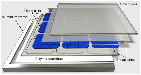
Figure 1.
Exploded view of a typical silicon PV module, showing the glass cover sheet, silicon cells, polymer encapsulant, polymer backsheet and aluminium frame.
In order to separate the module components, the module must first be deconstructed. A number of processes and techniques have been investigated for deconstruction of end-of-life crystalline silicon modules, including: mechanical crushing and shredding of the entire module, usually after removal of the aluminium frame; thermal decomposition of the backsheet and encapsulant followed by recovery of the wafers; and chemical and combined thermal–chemical removal of the backsheet and encapsulant with the aim of more comprehensive recovery of intact wafers [4,6,14,37,40,43,44,45,46].
Module crushing results in complete destruction of the silicon wafers and increased complications regarding materials separation, but is a relatively straightforward and chemically safe method for deconstruction of the module. Chemical and mechanical means can be used for separation of the useful materials from the resulting gravel, and a significant proportion of the total can be successfully extracted for addition to the relevant recycling and reprocessing streams [14,22,46]. In addition to complications regarding materials separation, the module crushing approach fails to allow for any reuse or direct refurbishing of the wafers.
Thermal or chemical decomposition of the polymer backsheet and encapsulant materials can, if done carefully, result in the recovery of intact wafers as well as relatively undamaged glass cover sheets and aluminium frames [24,37,38,45]. This can enable a number of options for reusing or reprocessing the silicon wafers. Thermal decomposition does however result in the generation of toxic gases, most notably hydrogen fluoride (HF), due to the fluorinated compounds typically used in backsheet polymers [22,38,47]. Much recent research has therefore focused on chemical and similar alternative means for removal of the backsheet and encapsulant. The primary goal of most of these methods is to cause delamination of the module through dissolution of the encapsulant, with the final module separation process then becoming relatively facile. Problems include obtaining initial access to the encapsulant; the slow rate at which the chemical process works, significantly slowing down the recycling process; and the increased use of chemicals such as nitric acid or organic solvents [7,22,25,38,48]. In addition, many of these processes do not fully remove the encapsulant, and therefore require subsequent heat treatments to burn off the remaining residue [22].
3.1. Recycling of Intact Silicon Wafers
Once the module has been delaminated, the glass and aluminium frame can be sent to the relevant recycling streams. Depending on the delamination process used, the wafers may still be connected in strings by the metal interconnects [22]. These interconnects are typically flat copper wires coated in a solder mix, traditionally consisting of tin and lead [27]. In order for further processing to take place, these interconnects first have to be removed through desoldering, after which they can be sent for further recycling and metals recovery [4,22,27,48]. Because lead is a toxic material, careful control of the interconnect wire recycling process is required in order to prevent environmental release [22,27,48]. A desoldering process may not be required if module delamination is achieved through thermal means however, since pyrolytic decomposition of the encapsulant and/or backsheet materials typically involves the use of sufficiently elevated temperatures that the cells can become desoldered at the same time [22,36]. These elevated temperatures can also be a problem in that modern cells are typically both thin and fragile, making them sensitive to thermal shock [4,22]. This is a potential concern with most commercially available furnaces, and could lead to a significant failure rate [22].
Once the wafers have been separated from the module, there are three options. The cells can be cleaned, checked to ensure they are still functional and retain an acceptable efficiency, re-soldered into strings and used directly in the construction of new modules. Alternatively, they can be used as silicon scrap, and entered into the silicon production process, or they can be treated using a number of chemical etching processes to produce “virgin” wafers, which can be used to synthesise new cells [4,7,11,20,22,24,36,38].
If the wafers are to be used as scrap for bulk silicon production, then the primary reason for keeping them intact is to make the materials separation process easier. Delamination is usually achieved using a thermal pyrolytic process, which causes the interconnects to become desoldered. This allows the interconnect wires to be removed from the wafers [20,36,43,48]. The silicon and glass fractions can then be sorted manually, by machine, or by a process such as density separation [43,45]. The wafers typically undergo further chemical treatments to remove the metal contacts, in particular the silver busbars, which whilst being a relatively minor fraction of the total module, are economically important [4,10,27,45]. Silver can be removed using a nitric acid or sulphuric acid etch followed either by electrolysis of the solution, or precipitation, which can be achieved through the addition of hydrochloric acid to the mixture [10,27,45,49,50,51,52]. Yang et al. suggested the use of a methanesulphonic acid-hydrogen peroxide mix as a more environmentally friendly alternative, with subsequent electrolytic recovery of the metal [51]. The back contact material is usually aluminium [22,27,48]. This can be removed using either a strong acid or a strong alkali, such as hydrochloric acid or sodium hydroxide [48,49,50]. Alternatives include the Loser Chemie process, which uses an aluminium chloride solution. This results in the formation of polyaluminium chlorides, which can be recovered and sold for use in waste water treatment [52]. Once the chemical removal of metals is complete, the silicon is ready for use in other processes, or further recycling and/or purification [4,11,43].
Specialised chemical treatments can be used to recover pristine silicon wafers, which can then be made into fresh cells using standard processes [13,19,49,50,53]. These treatments work by etching away any surface layers such as antireflective coatings and metal contacts followed by chemical leaching of the p- and n-type dopants to leave intrinsic silicon [49,50,53]. Park and Park used phosphoric acid to remove silicon nitride antireflective coatings and aluminium back contacts, whilst the silver busbars, emitter layer and dopants were removed using a mixture of hydrofluoric acid and nitric acid, leaving a pristine wafer [53]. Meanwhile, Klugmann-Radziemska et al. used nitric acid to remove the silver busbars, followed by potassium hydroxide or a potassium hydroxide–sodium hydroxide mix to etch the aluminium back contact layer [49,50]. The antireflective coating and dopants were removed using a number of different acid mixtures, with a mixture of nitric acid, hydrofluoric acid, acetic acid and bromine considered to be the best option for a universally applicable process [49,50]. The German company SolarWorld also used a wafer etching process of this type to recover high-purity silicon [19,42]. The SolarWorld recycling plant was operational from 2007 to 2012 [42]. As with some other commercial processes however, the precise details are difficult to obtain.
Whilst both promising and attractive, the wafer etching approach does have significant disadvantages. In particular, the use of different technologies and architectures in the manufacture of the original devices means that different chemical mixtures and process steps can be required for particular cells and cell types, making the entire process considerably more complex and potentially expensive [50]. In addition, some of the chemicals required are highly dangerous and environmentally hazardous [50]. Finally, the significant improvements in silicon cell technology over the past several decades have meant that silicon wafers used in the production of PV cells have become considerably thinner [4]. This gives rise to two problems. The use of thinner wafers means that modern cells are less robust, and even working modules have been found to exhibit significant levels of cell damage and wafer cracking [4,19,50]. Consequently, more modern modules are less likely to provide high yields of undamaged wafers, particularly since even the most gentle module deconstruction process is likely to result in further damage and hence wafer losses [19]. In addition the etching process required to remove unwanted parts of the original cell also removes some of the wafer material, which if the wafer is suitably thick to begin with would not be a problem, but for thinner wafers, could result in unacceptable levels of material loss and consequent low performance in reconstituted devices [4,50]. Nonetheless, these processes could have significant potential for the recovery of solar-grade silicon [4]. This is important because of the significantly higher value of solar grade silicon as compared with lower grades such as metallurgical silicon, meaning that processes which lead to its recovery could improve the overall economic case for module recycling [4,22].
3.2. Recycling of Crushed Modules
Whilst many current recycling processes crush or shred the modules, most do not separate out the silicon and polymeric materials from the glass [22,54]. Nonetheless, there are a number of procedures which do enable separation of the materials from crushed crystalline silicon modules. These processes typically use mechanical processing, either on its own or coupled with thermal and/or chemical treatments to enhance materials separation and recovery. Mechanical separation usually involves some form of sieving, although density separation has also been investigated [27,46]. Sieving or sifting as a separation process works on the basis that different materials tend to form different sizes of particle during the crushing and/or grinding process. Consequently, a vibrating sieve system can be used to perform separation and initial concentration of the materials, which for some processes might be considered sufficient, particularly if the polymeric materials have first been removed through a pyrolytic decomposition step [12,14,27]. In many cases however, additional processing, typically chemical or mechanochemical, is required to completely separate the different materials [12,14,27,46,54]. Separation by density can be achieved through the use of fluids with densities equivalent to or greater than some of the panel materials [27,46]. The use of water as the suspension medium is a potential problem, since only the polymer materials have a density equivalent to or less than water; however, this can be compensated for through the addition of salts such as sodium chloride or, for heavier materials, sodium polythungstate [27,46]. Alternatively, various fluid-mechanical methods similar to those used in mining can be employed [27].
Although a number of different processes and procedures have been developed and tested at a lab scale, relatively few have been implemented at either pilot-plant or full industrial scale. Examples include the Full Recovery End of Life Photovoltaic (FRELP) process and the Veolia process. The Italian company SASIL S.p.A developed the FRELP process, which has been implemented at a pilot scale [12,54]. This involves the removal of the aluminium frame and junction box, after which the panels are heated using an infrared source to between 90 and 120 °C [54]. The module is then run through a roller mill and vibrating knife machine, which removes the glass from the front of the module [12,54]. The glass is then sorted using a sieving process, whilst the remainder of the module is cut up further prior to undergoing a high temperature pyrolytic process to burn off the polymeric materials [12,54]. The resulting ash mixture is then sieved to remove any metal pieces, and then treated with nitric acid to etch out any remaining metals, including silver and copper [12,54]. The mixture is vacuum-filtered, and the leachate undergoes an electrowinning process followed by treatment with calcium hydroxide to recover the silver and copper fractions [12,54]. The recovered silicon is metallurgical (low) grade material [12,22,54]. An industrial full-scale silicon module specific recycling plant was built by Veolia in collaboration with PV_CYCLE in France in 2018 [22,55]. Veolia shred and then grind the panels into grit, after which they are put through a largely undisclosed mechanical process to separate out the different materials [22,55]. The procedure involves sifting the material, as well as an optical separation step, and enables significant separation of the silicon from the glass and polymer fractions. The process results in the complete recycling and reuse of about 95% of the module [42,55]. The reclaimed silicon is considered to be metallurgical (low grade) material [22].
3.3. Backsheet Polymers
Silicon module backsheets are typically laminates made from a range of different polymer materials. Many consist in whole or in part of fluorinated polymers such as polyvinyl fluoride (“Tedlar”), polyvinylidene fluoride or ethylene chlorotrifluoroethylene [8,40,47,50]. In recent years there has also been considerable interest in and movement towards the use of fluorine-free materials such as polyesters and polyamides. Investigation of the reliability and long-term structural stability of these fluorine-free polymers under the environmental conditions and timescales that PV modules encounter is a highly active research area [23,56]. From the perspective of the circular economy—an alternative to a traditional linear economy of take, make, use and dispose in which products and materials are kept in use as long as possible within closed loops—all of these materials are problematic [16,57,58,59,60]. Ideal materials can be recycled or reused indefinitely with no degradation or loss of properties [15,16]. Commonly recycled materials such as glass, aluminium and steel are excellent examples. The vast majority of plastics however either cannot be recycled at all, or else can only be recycled a certain number of times using current standard recycling processes [16]. The reason for this is that each time the material is processed, some degradation of the polymer chain occurs, resulting in gradual loss of the properties that make the material useful. Eventually, most plastics must be discarded or incinerated [16,57]. Both of these options have significant negative environmental effects. Discarded plastics are a major global concern with plastic waste, both macro and micro, found in every environment globally [57,61,62]. The very slow rate of degradation means that plastic waste will remain present for unacceptably long periods of time. Incineration removes this problem at the expense of increased gaseous pollution and greenhouse gas emissions [16,57]. If solar modules are to become fully recyclable, a key area for further research and development has to be environmentally benign and indefinitely recyclable materials for use as replacement backsheets.
Possible replacement materials for backsheet plastics include biopolymers such as modified starches, cellulose-based materials and polylactic acid (PLA) [63]. As with some oil-based plastics it is possible—although arguably economically challenging—to recycle some of these materials, in particular PLA, through a chemical recycling process, depolymerising the plastic to its constituent monomers and producing new material from the resulting feedstock [16,57,64]. Another advantage to using biopolymers is that, in the event that recycling cannot be carried out indefinitely, combustion of the materials would not lead to a net increase in carbon emissions, since the carbon used to produce the plastics is plant-based and therefore of recent (i.e., non-fossil-based) provenance. A significant area of concern in using these materials however is their long-term stability under a range of different environmental conditions. Since solar modules are intended to be used outdoors for multi-decade timespans, the backsheet polymers have to be sufficiently robust in order to minimise the risk of failure such as delamination, or embrittlement and cracking. These failure modes produce points or areas for the ingress of water, air and other environmental contaminants which can lead to cell damage and premature module failure [23,56]. It is therefore important that any new backsheet material is not just fully recyclable but is also able to survive under adverse environmental conditions for extended periods of time.
3.4. Encapsulant
The primary encapsulant material currently used in commercial solar modules is ethylene vinyl acetate (EVA), a copolymer of ethylene and vinyl acetate [37,39,65]. EVA is a relatively cheap and easy-to-handle material with good optical transparency which has been used in solar module construction for many years [39,65]. It is nonetheless known to be prone to aging through long-term exposure to outdoor environmental conditions, leading to discolouration and the release of small amounts of acetic acid [66,67,68]. The latter in particular can cause module damage through corrosion of metal interconnects and busbars, prematurely reducing module performance [67,68].
Because EVA is used as the encapsulant material, its removal is key to delamination of the module. The typical process most commonly discussed is therefore thermal treatment of the module, leading to thermal degradation and in some instances combustion of the EVA and backsheet materials [24,37,40]. Whilst enabling rapid deconstruction and separation of the remaining parts, this process does generate gaseous emissions, and precludes the possibility of recycling of the encapsulant. This problem can be avoided through chemical means, since EVA has been shown to dissolve or react with a number of solvents and solutions. These include substances such as toluene, xylene, sulphuric acid and lactic acid [44,46]. It is therefore plausible that at least some portion of the EVA could in theory be recycled through chemical means. Complete recycling of all of the EVA is unlikely to be achievable due to partial cross-linking of bonds within the material [27].
Because of the long-term degradation, discolouring and potential for module damage through acetic acid release, there has been considerable interest in alternatives to EVA in recent years [67,69]. The primary alternatives are types of polyolefin, including thermoplastic polyolefins (TPO) and polyolefin elastomers (POE) [67,69]. Both types of material have been demonstrated to show improved environmental stability, and due to the lack of the vinyl acetate side-group, acetic acid is not generated during module use [67]. As with potential backsheet replacement materials however, fully circular recycling of these polyolefin plastics may be problematic unless efficient chemical recycling can be implemented at scale.
4. CdTe and CIGS
CdTe and CIGS modules present some additional complications when compared with the typical crystalline silicon modules. The primary difference is that both cell types are deposited as a series or stack of thin films onto a substrate, typically glass. This means that unlike crystalline silicon modules, the cells cannot be separated from the panel simply through delamination of the encapsulant. A number of the elements which make up these cell types are toxic, in particular cadmium (present in both the CdTe absorber layer and in cadmium sulphide window layers), selenium (present in the CIGS absorber material) and tellurium (present in the CdTe absorber) [44,70,71,72]. Recycling of these module types therefore has to include careful environmental controls in order to prevent accidental release of these materials [70]. A further complication with these types of module is that a number of the constituent materials are rare, experience high levels of demand, or both [34,45,71,73,74]. It has been suggested that since cadmium telluride is reasonably chemically stable, and the potential long-term cadmium emissions are significantly lower than from other energy generation technologies, placing end-of-life modules in landfill is both a more economic option, and represents a relatively low environmental risk; however recycling was still found to have a higher environmental benefit [72]. Additionally, the value and rarity of some of the materials present in these modules, the increase in legislation making recycling mandatory and the number of possible industrially scalable methods for recycling these modules mean that landfill-based disposal is increasingly undesirable as a long-term solution.
Construction of both CdTe and CIGS module types typically involves the use of a glass front panel, encapsulant, and either a glass backsheet or occasionally in the case of CdTe a polymer or metal backsheet. For CdTe modules, the front glass sheet is normally the substrate (or more accurately the superstrate) onto which the cells are deposited, whilst for CIGS modules, the rear sheet is typically used as the substrate [72] (Figure 2). Recycling of both module types can involve either mechanical crushing of the module, or separation of the module through a delamination process (thermal, chemical or a combination) [7,14,45,72]. As with silicon modules, EVA is usually used as the module encapsulant. Once the initial processing has taken place, extraction of the different constituent materials can commence. This can include solvent or reactant-based leaching of specific materials, mechanical separation and froth flotation, or electrochemical separation and electrowinning [29,72,75,76,77].
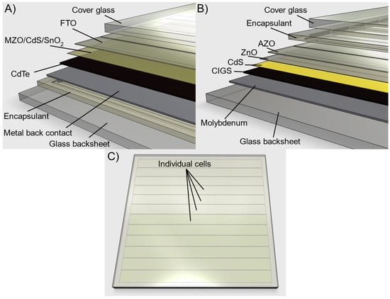
Figure 2.
(A) CdTe module structure, formed using the cover glass as a superstrate. A number of different materials can be used as the window layer; typical materials used are given. FTO is fluorine-doped tin oxide, the typical transparent conductor used in CdTe devices, and MZO is magnesium zinc oxide. (B) CIGS module structure. These devices use a substrate system and are deposited onto a metal (typically molybdenum) coated glass backsheet. AZO is aluminium-doped zinc oxide, the transparent conductor typically used in CIGS devices. (C) Diagram showing how a thin film module appears when complete.
4.1. CdTe Recycling
The current process used for the end-of-life recycling of most CdTe panels is that employed by the company First Solar [28,29,30,32,35,78,79]. This process begins with shredding and then crushing of the panels to generate a gravel with particulate sizes of less than 12 mm, and typically nearer 4–5 mm [29,35,78]. The particulate size is important because pieces of this size are small enough to ensure that the bond between the cells and the encapsulant has been sufficiently broken to allow for ingress of leaching fluids [26,30]. The material is then fed into a rotating drum reactor, where it is treated using a solution containing sulphuric acid and hydrogen peroxide as the primary reagents [29,30,35,78]. The mechanical agitation is considered to increase the leaching rate through further reduction in particulate size, as well as through some mechanical removal of the semiconductor films from the glass surface [30]. Once the leaching process is complete, the slurry is filtered to separate the leachate from the solid fraction. The undissolved solids primarily comprise glass and encapsulant and, following separation from the leachate, these are sieved using a vibrating screen array [30,78]. Because glass is more friable than the polymeric encapsulant, the glass particulates are typically smaller; the sieving process therefore enables significant separation of the two [30,78]. The solids are then washed to remove residual traces of the leachate. Once suitably cleaned, the glass portion is usually resold as glass cullet [30,78]. The leachate is treated using a series of progressively more alkaline solutions, either of sodium carbonate or, more recently, sodium hydroxide [29,30,32,72,78]. The primary benefit of using sodium hydroxide is that it has a slightly higher materials recovery rate, in particular for tellurium [32]. The precipitate is concentrated in a thickening tank, dewatered, and the solids are dried, packaged and sent for further processing by a third party [30,32,72,78]. The liquid is filtered to remove any remaining particulates, passed through an ion exchange resin to remove any residual cadmium and tellurium, and discarded [30]. This process results in very high recovery rates of both cadmium and tellurium, with a leaching efficiency of about 99% and a precipitation efficiency of greater than 99.6% [32,35].
Possible alternatives to the process used by First Solar include simple mechanical scraping of the material from the glass substrate; use of combined mechanical and hydraulic or mechanical and chemical means to cause separation of the semiconductor films from the glass; or the use of alternative chemical reactions or dissolution processes followed by subsequent recovery through chemical or electrochemical means [26,28,29,31,33,72,77,79]. The American company Drinkard Metalox and the German company ANTEC Solar have both developed chemical processes which have been used in pilot-scale plants [31,33,72]. The Drinkard Metalox process involves the use of nitric acid as the leaching reagent [31,72]. Polymeric materials, such as the encapsulant, are skimmed from the surface of the liquid. Following decanting and filtering of the liquid, the glass is rinsed, dried and can be sold as glass cullet. Tellurium is obtained from the leachate by electrowinning, and evaporation of the remaining liquid enables recovery of the cadmium [31]. The ANTEC Solar process was invented with the aim of minimising wet-chemical procedures [33]. Whilst the modules are first crushed, the particle size requirements are considerably more relaxed than for the First Solar process [33]. Once the modules have been crushed the material is heated, resulting in the pyrolytic decomposition of the encapsulant. This is followed by exposure of the remaining materials to a gas mix containing chlorine at an elevated temperature of more than 400 °C [4,33]. The chlorine gas and elevated temperatures result in an etching process whereby the cadmium and tellurium react with the chlorine to form their respective chlorides and evaporate. The chloride-enriched gases are then extracted and cooled, leading to condensation of the respective chlorides, at which point they can be recovered [33]. Separation of the tellurium and cadmium can be achieved through the use of two or more cooling traps held at different temperatures, since the two chlorides have different condensation points [33].
4.2. CIGS Recycling
As with CdTe recycling, there are a number of possible means for recycling CIGS modules, most of which involve some form of chemical etching and refining. Unlike CdTe however, there is no single established system for recycling of end-of-life modules [72]. To date the only companies with established recycling processes explicitly designed for CIGS materials appear to be Umicore (Belgium) and 5N Plus (Canada); unfortunately, details of their processes are challenging to obtain [72,73,80]. CIGS recycling processes have been developed for both crushed and delaminated modules.
Kushiya et al. demonstrated a mixed chemical–mechanical method for recycling CIGS modules [81]. The module is initially delaminated by heating to soften the encapsulant, after which the surface glass sheet is pushed off the top [72,81]. The remaining encapsulant material is then removed using an acetic acid bath. This causes both swelling of the EVA encapsulant and dissolution of the zinc oxide-based buffer and window layers, thereby separating the encapsulant from the module [72,81]. The remaining part of the module is then dried, and the semiconductor materials are removed using a mechanical scribing technique. This involves the use of a metal blade coupled with a vacuum extraction unit to remove the dust [81]. The process is particularly effective due to the thin molybdenum diselenide layer present at the back of the cell [81]. This is typically present in CIGS cells since it helps to form a good ohmic contact between the CIGS material and the molybdenum back contact. When using a mechanical process to remove the CIGS however, it acts as a solid lubricant, thereby improving the efficacy of the process [81]. Once the CIGS has been removed, the molybdenum coated glass can either be washed and reused, or else the molybdenum can be dissolved using a nitric acid solution.
The American company Drinkard Metalox developed a process which bears a remarkable similarity to their CdTe process [82,83]. If a laminated module is to be recycled, it is first crushed or shredded. The gravel is then placed in a nitric acid bath, which reacts with the semiconductor and metal components [82,83]. The polymer encapsulant material is skimmed from the top of the liquid [82]. If unlaminated modules are used, they can be placed directly into the acid bath without crushing, since the semiconductor materials are already exposed [82]. The mix is warmed to increase the reaction rate. Once the semiconductor materials have completely dissolved, the mixture is decanted and filtered to separate the glass cullet from the liquid. The glass can then be washed and recycled. The semiconductor components are retrieved from the liquid through a series of electrolytic processes [82,83]. Initially, copper and selenium are retrieved from the solution. Once the leachate is depleted in copper and selenium the electrode is replaced, after which cadmium is deposited. Evaporation of the remaining liquid enables recovery of zinc and indium nitrates. The copper-selenium mix is separated either through roasting the mixture in the presence of sulphuric acid, which produces copper sulphate and selenium dioxide, or through dissolution in nitric acid, after which the selenium is converted to selenium dioxide. The selenium dioxide can then be recovered through a high-temperature distillation process [82,83]. Gu et al. demonstrated a similar process for the dissolution and recovery of the CIGS component materials [84]. Rather than nitric acid however, this used a hydrochloric acid—hydrogen peroxide mix. This enables electrolytic recovery of the selenium and copper separately rather than as a mixture [84]. The remaining liquid was distilled to extract unreacted hydrogen chloride, with indium and gallium chlorides crystallising out [84]. Electrolytic refining has also been shown to enable separation and recovery of each of the individual elements in the CIGS material [83,85,86]. This does rely on the use of module delamination rather than crushing, but unlike many of the proposed processes, enables complete materials separation [83]. Alternative chemical approaches typically begin with the removal and retrieval of the selenium. This can be achieved through electrowinning, chemical etching, or thermal oxidation followed by dissolution and reduction of the oxide using either an organic reducing agent or sulphur dioxide [73,83,86]. Gustafsson et al. demonstrated a thermal oxidation-reduction process for the extraction of selenium from CIGS powder which allows for the recovery of high-purity selenium, with values of four to five nines pure [83]. A notable disadvantage of this process is that in order to achieve acceptable recovery rates, high temperatures are required. The tested materials were ground from spent sputtering targets, and no glass or polymeric materials were present [83]. Nonetheless, this could usefully be applied to the separated semiconductor materials extracted using a mechanical process such as that described by Kushiya et al. [81]. Once the selenium has been extracted, the indium, gallium and copper can be etched or dissolved followed by reprecipitation, or removed through an electrowinning process, or a combination [44,73,86]. Thermal chlorination is another alternative method which has been suggested as a means for separating the remaining metals [75]. This is a variation of an industrially used process for separation of metals through the high-temperature formation and subsequent distillation of volatile metal chlorides [75]. Ammonium chloride was used as the chlorination reagent. The metal chlorides could be extracted separately due to their varying reaction kinetics and evaporation temperatures [75]. Gallium chloride was extracted first, followed by indium chloride and finally copper chloride. Each material was condensed prior to dissolution and extraction with water. The small residual selenium fraction was found to precipitate during the extraction process [75]. Although separation was largely achieved, each fraction was found to contain some of at least one of the other two fractions. Additionally, a considerable amount of ammonium chloride was found to be required. Further development would therefore be necessary before it could be employed as an industrial recycling process [75].
5. Combined Recycling Methods
Another group of procedures have been developed which aim to enable recycling of photovoltaic modules of different types and technologies [14,26,29,52,87]. Most of these processes are applicable to CIGS and CdTe, and can be used for either technology type, with a few other processes also including crystalline silicon. Modules are either crushed directly or undergo thermal treatment prior to crushing to pyrolytically decompose the encapsulant [14,26,29,52,54]. The semiconductor materials are then separated from the glass particulates using wet mechanical methods, sieving, a vacuum blasting process, or a combination [26,29]. Vacuum blasting uses a vacuum to cause blasting media to abrade the semiconductor materials, thereby removing them from the glass. The blasting medium and semiconductor particulates are removed together, and the glass and encapsulant can be washed and separated using a vibrating screen system [26,29,30]. Wet mechanical separation typically involves the use of an intensive mixing process, whereby the crushed material is mixed with water and rapidly agitated. This leads to the complete or near-complete removal of the semiconductor layers from the glass through shearing and friction forces [26,29]. Separation and removal of the semiconductor materials from the glass cullet or from the vacuum blasting medium is then achieved through the use of flotation and/or froth-flotation techniques equivalent to those used in the mining industry [26,29]. The flotation concentrate containing the semiconductor materials is then ready for further processing in order to recover the constituent elements. This can be achieved either through dewatering, drying and then smelting of the filter cake, or through the use of chemical reaction and dissolution processes similar to those described previously [26,29]. The Photolife process involves sieving the crushed panel materials to produce three fractions based on grain size: a coarse fraction, defined as pieces with greater than 1 mm diameter; an intermediate fraction, defined as 0.1 to 1 mm; and a fine fraction, defined as anything less than 0.1 mm [14,54,87]. The coarse fraction was found to contain the majority of the polymeric encapsulant and backsheet materials, and so is treated either using a thermal combustion process or by washing with a cyclohexane–acetone mixture to dissolve the polymers [14,54,87]. Further sieving of the remaining solids enables separation of the metal interconnect materials from the glass and semiconductor fractions. The intermediate fraction typically consists of clean glass, and can be recovered as glass cullet [87]. The fine fraction is treated using either a sequential alkaline leaching process, or an oxidising acid process. The alkaline process uses sodium hydroxide solutions of varying pH to preferentially etch different materials, notably cadmium, tellurium, zinc and aluminium, with the specific elements depending on the module type [54,87]. Alternatively, a mixed solution of sulphuric acid and hydrogen peroxide with a pH of less than six can be used. The leachate and remaining solids are then separated, and the dissolved elements are recovered through a series of electrowinning and precipitation processes [54,87]. The remaining solids, which depending on the panel type contain materials such as glass, silicon, silver and titanium, can be sent for further chemical processing for the selective recovery of the constituent materials [87].
6. Future Directions
It has been shown that recovery of all of the non-polymeric constituent materials in a silicon module is possible in some form, but not always with the ideal levels of purity. In particular, most processes either fail to extract the silicon at all, or else produce metallurgical grade material which needs further refining prior to use in new cell manufacturing. Existing processes which do give the higher-value and more useful solar-grade silicon are complex, often specific to a particular type and architecture of cell, and require the use of dangerous and unpleasant chemicals such as hydrofluoric acid [49,50]. The additional cost, safety issues and complexity may explain why these processes have not yet been applied industrially, despite the considerably higher prices commanded by solar-grade silicon [22]. Nonetheless, some development of industrial-scale processes to produce improved purities of silicon and other panel materials is taking place, with a consortium managed by Veolia currently undertaking a series of feasibility tests [88]. The integration of some of the wafer processing techniques into existing processes and the development of lower-cost and safer means for the recovery of high-grade silicon from spent panels therefore remain attractive and important areas for further research.
The primary means for recycling CdTe panels, run by First Solar, appears to be highly effective and results in the recovery of the overwhelming majority of the semiconductor materials. These are sent to a third party for refining to the required purity levels, prior to their re-incorporation into the module manufacturing processes [78]. The glass is sold off as clean cullet. This process is already well established industrially and leads to recovery of nearly all materials apart from the encapsulant.
Because of the lack of published information, it is difficult to determine the ways in which the two industrial CIGS processes might be improved, and there is little indication of which materials are recovered and no details of their respective purities. Nonetheless, a number of processes have been tested at a laboratory scale which demonstrate that all of the materials in a CIGS module can be recovered effectively, with the exception of the encapsulant. The extent to which these processes could be economically viable in an industrial setting is unknown and may represent an opportunity for further work.
The primary set of materials which none of the published processes appear to recycle in any meaningful way are the polymers, notably the panel encapsulant (usually EVA) and the backsheet. The lack of interest in the recycling of these materials is most likely due to their being both difficult to recycle and of low economic value [27]. This could be improved through the targeted development of materials appropriate for this application but which are also more readily recyclable. However, identifying materials which can be removed and fully recycled easily whilst simultaneously being sufficiently adherent and environmentally robust over the expected lifetime of the module represents a significant challenge. It is also possible new polymer materials might complicate future recycling efforts, given that different materials may require different processing procedures. Nonetheless, any development which leads to these materials being recycled would be an improvement on the current situation. Development of alternative encapsulant and backsheet polymer materials which can be fully recycled relatively easily therefore has potential as an area for further research. Another approach could be the development of robust materials synthesised from plant matter, which can then be burned during the recycling process without causing a net increase in carbon emissions.
7. Conclusions
This paper has outlined the primary methods available for recycling of photovoltaic panels, including both the more common crystalline silicon modules as well as CdTe and CIGS thin film modules. A summary of the methods discussed is presented in Table 1.

Table 1.
Summary of the different recycling processes for each module type.
The most common method currently used for recycling photovoltaic modules is to remove the junction box and aluminium frame, crush the module and use it as mixed glass cullet. This enables the use of existing recycling facilities but precludes the recovery of any of the more valuable semiconductor materials and metals. A number of more complex processes have been devised for recycling of crystalline silicon modules, with a mechanical separation process being used in one industrially operational process, and a thermal–mechanical–chemical process being evaluated at a pilot scale. Other options include means for module delamination rather than crushing, followed by chemical processing of the wafers to recover some of the metals, notably silver, and to remove surface coatings and dopants. Most of the processes currently in use industrially either fail to recover the silicon at all or produce metallurgical grade material. Application of some of the wafer processing techniques could enable recovery of solar (high-grade) silicon, which is considerably more valuable, and might thereby improve the economics of recycling. Alternatively, the economic recovery of higher grades of silicon from crushed material is conceivably achievable, and represents an interesting and potentially valuable area for future research.
Most CdTe modules are currently recycled by First Solar, using their own mechano-chemical process. This involves crushing the modules, chemical leaching of the cell materials, a sieving process to separate out the glass and polymer fractions, and a chemical recovery process to extract the semiconductor materials and metals. Most alternative processes also involve crushing of the module followed by chemical processing, either in liquid form or through reaction with gases at high temperatures.
CIGS is currently recycled industrially by two companies, but the precise details of the processes employed are challenging to obtain. A number of published processes do exist, most of which have been tested at laboratory scale only. As with CdTe, most of these involve crushing of the module followed by chemical processing of the semiconductor materials. This includes leaching followed by electrochemical recovery, or thermal removal of selenium followed by chlorination of the metals and their recovery through sequential evaporation of the resulting chlorides. There are also several suggested processes which involve module delamination, after which the cell materials are removed either through a mechanical scraping process or through sequential electrolytic extraction.
A small number of methods have been developed for the recycling of two or more module types. These typically include separation and removal of the semiconductor materials through the use of vacuum blasting or wet mechanical processes, or a combination of wet mechanical and chemical processing.
Another area for further research is in the development of processes which enable recycling of the encapsulant and backsheet polymers, and into the development of environmentally benign alternatives to the polymer materials currently used. The use of new polymer materials both as backsheets and as encapsulants may complicate future recycling efforts however, since different materials are likely to require different recycling processes. Development of a standardised set of materials which are known to both protect the module during its expected lifetime and which can readily be recycled would be the optimal means of avoiding this problem.
7.1. Limitations
As with any review, it is not possible to cover every published process and technique in the field. Consequently, this paper is limited to known processes which are currently used industrially, and those which have received significant or notable discussion in the literature. It is therefore entirely plausible that processes which will become important in the future, but which are still at the experimental stage today, have not been included in this work. There are also several important procedures and suggested means for the recycling of photovoltaic modules for which the precise details are not readily available. These are typically processes which have been developed partially or wholly by commercial entities, and the exact means by which the module recycling takes place have not been publicly disclosed. Whilst care has been taken to include as much information as possible regarding these processes, the lack of published details has made this particularly challenging. Acknowledgement of this problem is included where these processes are discussed in the text. Finally, the criteria used for selection of literature sources may have led to the exclusion of material which could otherwise have been useful or significant. In particular the requirement for material to have been published by a known entity or author, or in a journal or proceedings which are known and recognised in the field, could have led to the exclusion of some potentially valuable sources. This limitation was accepted as necessary in order to minimise the risk of including spurious or unverified processes and claims.
Funding
This research received no external funding.
Institutional Review Board Statement
Not applicable.
Informed Consent Statement
Not applicable.
Data Availability Statement
Not applicable.
Acknowledgments
The author would like to thank Kyungeun Sung for the opportunity to publish this work, and for her assistance and support during the writing process.
Conflicts of Interest
The author declares no conflict of interest.
References
- MacKay, D.J.C. Sustainable Energy—Without the Hot Air; UIT Cambridge Ltd.: Cambridge, UK, 2009; ISBN 9780954452933. [Google Scholar]
- IEA. Solar PV.; IEA: Paris, France, 2020. [Google Scholar]
- BP. BP Statistical Review of World Energy; BP: London, UK, 2019. [Google Scholar]
- Heath, G.A.; Silverman, T.J.; Kempe, M.; Deceglie, M.; Ravikumar, D.; Remo, T.; Cui, H.; Sinha, P.; Libby, C.; Shaw, S.; et al. Research and development priorities for silicon photovoltaic module recycling to support a circular economy. Nat. Energy 2020, 5, 502–510. [Google Scholar] [CrossRef]
- Deng, R.; Chang, N.L.; Ouyang, Z.; Chong, C.M. A techno-economic review of silicon photovoltaic module recycling. Renew. Sustain. Energy Rev. 2019, 109, 532–550. [Google Scholar] [CrossRef]
- Sica, D.; Malandrino, O.; Supino, S.; Testa, M.; Lucchetti, M.C. Management of end-of-life photovoltaic panels as a step towards a circular economy. Renew. Sustain. Energy Rev. 2018, 82, 2934–2945. [Google Scholar] [CrossRef]
- Maani, T.; Celik, I.; Heben, M.J.; Ellingson, R.J.; Apul, D. Environmental impacts of recycling crystalline silicon (c-SI) and cadmium telluride (CDTE) solar panels. Sci. Total Environ. 2020, 735, 138827. [Google Scholar] [CrossRef]
- Ardente, F.; Latunussa, C.E.L.; Blengini, G.A. Resource efficient recovery of critical and precious metals from waste silicon PV panel recycling. Waste Manag. 2019, 91, 156–167. [Google Scholar] [CrossRef]
- Cucchiella, F.; D’Adamo, I.; Rosa, P. End-of-Life of used photovoltaic modules: A financial analysis. Renew. Sustain. Energy Rev. 2015, 47, 552–561. [Google Scholar] [CrossRef]
- Dias, P.; Javimczik, S.; Benevit, M.; Veit, H.; Bernardes, A.M. Recycling WEEE: Extraction and concentration of silver from waste crystalline silicon photovoltaic modules. Waste Manag. 2016, 57, 220–225. [Google Scholar] [CrossRef]
- Deng, R.; Chang, N.; Lunardi, M.M.; Dias, P.; Bilbao, J.; Ji, J.; Chong, C.M. Remanufacturing end-of-life silicon photovoltaics: Feasibility and viability analysis. Prog. Photovolt. Res. Appl. 2021, 29, 760–774. [Google Scholar] [CrossRef]
- Latunussa, C.E.L.; Ardente, F.; Blengini, G.A.; Mancini, L. Life Cycle Assessment of an innovative recycling process for crystalline silicon photovoltaic panels. Sol. Energy Mater. Sol. Cells 2016, 156, 101–111. [Google Scholar] [CrossRef]
- Padoan, F.C.S.M.; Altimari, P.; Pagnanelli, F. Recycling of end of life photovoltaic panels: A chemical prospective on process development. Sol. Energy 2019, 177, 746–761. [Google Scholar] [CrossRef]
- dos Santos Martins Padoan, F.C.; Schiavi, P.G.; Belardi, G.; Altimari, P.; Rubino, A.; Pagnanelli, F. Material Flux through an Innovative Recycling Process Treating Different Types of End-of-Life Photovoltaic Panels: Demonstration at Pilot Scale. Energies 2021, 14, 5534. [Google Scholar] [CrossRef]
- McDonough, W.; Braungart, M. Cradle to Cradle: Remaking the Way We Make Things; Vintage: London, UK, 2008; ISBN 9781784873653. [Google Scholar]
- Helms, B.A.; Russell, T.P. Reaction: Polymer Chemistries Enabling Cradle-to-Cradle Life Cycles for Plastics. Chem 2016, 1, 816–818. [Google Scholar] [CrossRef] [Green Version]
- Chopra, K.L.; Paulson, P.D.; Dutta, V. Thin-film solar cells: An overview. Prog. Photovolt. Res. Appl. 2004, 12, 69–92. [Google Scholar] [CrossRef]
- Luque, A.; Hegedus, S. (Eds.) Handbook of Photovoltaic Science and Engineering, 2nd ed.; John Wiley & Sons: Chichester, UK, 2011; ISBN 9780470721698. [Google Scholar]
- Tao, J.; Yu, S. Review on feasible recycling pathways and technologies of solar photovoltaic modules. Sol. Energy Mater. Sol. Cells 2015, 141, 108–124. [Google Scholar] [CrossRef]
- Bohland, J.R.; Anisimov, I. Possibility of Recycling Silicon PV Modules. In Conference Record of the Twenty Sixth IEEE Photovoltaic Specialists Conference—1997; IEEE: Manhattan, NY, USA, 1997; pp. 1173–1175. [Google Scholar]
- Müller, A.; Wambach, K.; Alsema, E. Life cycle analysis of solar module recycling process. Mater. Res. Soc. Symp. Proc. 2006, 895, 89–94. [Google Scholar] [CrossRef]
- Tao, M.; Fthenakis, V.; Ebin, B.; Steenari, B.M.; Butler, E.; Sinha, P.; Corkish, R.; Wambach, K.; Simon, E.S. Major challenges and opportunities in silicon solar module recycling. Prog. Photovolt. Res. Appl. 2020, 28, 1077–1088. [Google Scholar] [CrossRef]
- Julien, S.E.; Kim, J.H.; Lyu, Y.; Miller, D.C.; Gu, X.; Wan, K.t. Cohesive and adhesive degradation in PET-based photovoltaic backsheets subjected to ultraviolet accelerated weathering. Sol. Energy 2021, 224, 637–649. [Google Scholar] [CrossRef]
- Wang, T.Y.; Hsiao, J.C.; Du, C.H. Recycling of materials from silicon base solar cell module. In Proceedings of the 2012 38th IEEE Photovoltaic Specialists Conference, Austin, TX, USA, 3–8 June 2012; pp. 2355–2358. [Google Scholar] [CrossRef]
- Pang, S.; Yan, Y.; Wang, Z.; Wang, D.; Li, S.; Ma, W.; Wei, K. Enhanced separation of different layers in photovoltaic panel by microwave field. Sol. Energy Mater. Sol. Cells 2021, 230, 111213. [Google Scholar] [CrossRef]
- Marchetti, B.; Corvaro, F.; Giacchetta, G.; Polonara, F.; Cocci Grifoni, R.; Leporini, M. Double Green Process: A low environmental impact method for recycling of CdTe, a-Si and CIS/CIGS thin-film photovoltaic modules. Int. J. Sustain. Eng. 2018, 11, 173–185. [Google Scholar] [CrossRef]
- Dias, P.; Veit, H. Recycling Crystalline Silicon Photovoltaic Modules. In Emerging Photovoltaic Materials: Silicon & Beyond; Kurinec, S.K., Ed.; Scrivener Publishing: Beverley, MA, USA, 2018; pp. 61–102. [Google Scholar]
- Bohland, J.; Anisimov, I.; Dapkus, T. Economic recycling of CdTe photovoltaic modules. In Conference Record of the Twenty Sixth IEEE Photovoltaic Specialists Conference—1997; IEEE: Manhattan, NY, USA, 1997; pp. 355–358. [Google Scholar] [CrossRef]
- Berger, W.; Simon, F.G.; Weimann, K.; Alsema, E.A. A novel approach for the recycling of thin film photovoltaic modules. Resour. Conserv. Recycl. 2010, 54, 711–718. [Google Scholar] [CrossRef]
- Bohland, J.R.; Anisimov, I.I.; Dapkus, T.J.; Sasala, R.A.; Smigielski, K.A.; Kamm, K.D. Reclaiming Metallic Material from an Article Comprising a Non-Metallic Friable Substrate. U.S. Patent 6,129,779, 10 October 2000. [Google Scholar]
- Goozner, R.E.; Long, M.O.; Drinkard, W.F. Recycling of CdTe Photovoltaic Waste. U.S. Patent 5,897,685, 27 April 1999. [Google Scholar]
- Mezei, A.; Ashbury, M.; Canizares, M.; Molnar, R.; Given, H.; Meader, A.; Squires, K.; Ojebuoboh, F.; Jones, T.; Wang, W. Hydrometallurgical recycling of the semiconductor material from photovoltaic materials—Part one: Leaching. In Hydrometallurgy 2008: Proceedings of the Sixth International Symposium; SME: Englewood, CO, USA, 2008; pp. 209–220. [Google Scholar]
- Campo, M.D.; Bonnet, D.; Gegenwart, R.; Beier, J. Process for Recycling CdTe/CdS Thin Film Solar Cell Modules. U.S. Patent 6,572,782, 3 June 2003. [Google Scholar]
- Rocchetti, L.; Beolchini, F. Recovery of valuable materials from end-of-life thin-film photovoltaic panels: Environmental impact assessment of different management options. J. Clean. Prod. 2015, 89, 59–64. [Google Scholar] [CrossRef]
- Mezei, A.; Ashbury, M.; Canizares, M.; Molnar, R.; Given, H.; Meader, A.; Squires, K.; Ojebuoboh, F.; Jones, T.; Wang, W. Hydrometallurgical recycling of the semiconductor material from photovoltaic materials—Part two: Metal recovery. In Hydrometallurgy 2008: Proceedings of the Sixth International Symposium; SME: Englewood, CO, USA, 2008; pp. 224–237. [Google Scholar]
- Bohland, J.R.; Anisimov, I.I. Recycling Silicon Photovoltaic Modules. U.S. Patent 6,063,995, 16 May 2000. [Google Scholar]
- Zeng, D.W.; Born, M.; Wambach, K. Pyrolysis of EVA and its application in recycling of photovoltaic modules. J. Environ. Sci. 2004, 16, 889–893. [Google Scholar]
- Xu, X.; Lai, D.; Wang, G.; Wang, Y. Nondestructive silicon wafer recovery by a novel method of solvothermal swelling coupled with thermal decomposition. Chem. Eng. J. 2021, 418, 129457. [Google Scholar] [CrossRef]
- Chitra; Sah, D.; Lodhi, K.; Kant, C.; Saini, P.; Kumar, S. Structural composition and thermal stability of extracted EVA from silicon solar modules waste. Sol. Energy 2020, 211, 74–81. [Google Scholar] [CrossRef]
- Fiandra, V.; Sannino, L.; Andreozzi, C.; Corcelli, F.; Graditi, G. Silicon photovoltaic modules at end-of-life: Removal of polymeric layers and separation of materials. Waste Manag. 2019, 87, 97–107. [Google Scholar] [CrossRef]
- Skoczek, A.; Sample, T.; Dunlop, E.D. The results of performance measurements of field-aged crystalline silicon photovoltaic modules. Prog. Photovolt. Res. Appl. 2009, 17, 227–240. [Google Scholar] [CrossRef]
- Tsanakas, J.A.; van der Heide, A.; Radavičius, T.; Denafas, J.; Lemaire, E.; Wang, K.; Poortmans, J.; Voroshazi, E. Towards a circular supply chain for PV modules: Review of today’s challenges in PV recycling, refurbishment and re-certification. Prog. Photovolt. Res. Appl. 2020, 28, 454–464. [Google Scholar] [CrossRef]
- Ansanelli, G.; Fiorentino, G.; Tammaro, M.; Zucaro, A. A Life Cycle Assessment of a recovery process from End-of-Life Photovoltaic Panels. Appl. Energy 2021, 290, 116727. [Google Scholar] [CrossRef]
- Savvilotidou, V.; Antoniou, A.; Gidarakos, E. Toxicity assessment and feasible recycling process for amorphous silicon and CIS waste photovoltaic panels. Waste Manag. 2017, 59, 394–402. [Google Scholar] [CrossRef]
- Savvilotidou, V.; Gidarakos, E. Pre-concentration and recovery of silver and indium from crystalline silicon and copper indium selenide photovoltaic panels. J. Clean. Prod. 2020, 250, 119440. [Google Scholar] [CrossRef]
- Azeumo, M.F.; Conte, G.; Ippolito, N.M.; Medici, F.; Piga, L.; Santilli, S. Photovoltaic module recycling, a physical and a chemical recovery process. Sol. Energy Mater. Sol. Cells 2019, 193, 314–319. [Google Scholar] [CrossRef]
- Geretschläger, K.J.; Wallner, G.M.; Fischer, J. Structure and basic properties of photovoltaic module backsheet films. Sol. Energy Mater. Sol. Cells 2016, 144, 451–456. [Google Scholar] [CrossRef]
- Wang, T.Y. Recycling Solar Cell Materials at the End of Life. In Advances in Solar Photovoltaic Power Plants; Islam, M.R., Rahman, F., Xu, W., Eds.; Springer: Berlin/Heidelberg, Germany, 2016; pp. 287–317. ISBN 9783662505199. [Google Scholar]
- Klugmann-Radziemska, E.; Ostrowski, P.; Drabczyk, K.; Panek, P.; Szkodo, M. Experimental validation of crystalline silicon solar cells recycling by thermal and chemical methods. Sol. Energy Mater. Sol. Cells 2010, 94, 2275–2282. [Google Scholar] [CrossRef]
- Klugmann-Radziemska, E.; Ostrowski, P. Chemical treatment of crystalline silicon solar cells as a method of recovering pure silicon from photovoltaic modules. Renew. Energy 2010, 35, 1751–1759. [Google Scholar] [CrossRef]
- Yang, E.H.; Lee, J.K.; Lee, J.S.; Ahn, Y.S.; Kang, G.H.; Cho, C.H. Environmentally friendly recovery of Ag from end-of-life c-Si solar cell using organic acid and its electrochemical purification. Hydrometallurgy 2017, 167, 129–133. [Google Scholar] [CrossRef]
- Palitzsch, W.; Loser, U. Systematic photovoltaic waste recycling. Green 2013, 3, 79–82. [Google Scholar] [CrossRef]
- Park, J.; Park, N. Wet etching processes for recycling crystalline silicon solar cells from end-of-life photovoltaic modules. RSC Adv. 2014, 4, 34823–34829. [Google Scholar] [CrossRef]
- Komoto, K.; Lee, J.S. End-of-Life Management of Photovoltaic Panels: Trends in PV Module Recycling Technologies; National Renewable Energy Lab.: Golden, CO, USA, 2018.
- Veolia SA Press Release. Veolia Open the First European Plant Entirely Dedicated to Recycling Photovoltaic Panels. Available online: https://www.veolia.com/en/newsroom/news/recycling-photovoltaic-panels-circular-economy-france (accessed on 7 December 2021).
- Ulicna, S.; Sinha, A.; Springer, M.; Miller, D.C.; Hacke, P.; Schelhas, L.T.; Owen-Bellini, M. Failure Analysis of a New Polyamide-Based Fluoropolymer-Free Backsheet after Combined-Accelerated Stress Testing. IEEE J. Photovolt. 2021, 11, 1197–1205. [Google Scholar] [CrossRef]
- Jubinville, D.; Esmizadeh, E.; Saikrishnan, S.; Tzoganakis, C.; Mekonnen, T. A comprehensive review of global production and recycling methods of polyolefin (PO) based products and their post-recycling applications. Sustain. Mater. Technol. 2020, 25, e00188. [Google Scholar] [CrossRef]
- Ellen MacArthur Foundation. Towards the Circular Economy: Economic and Business Rationale for an Accelerated Transition; Ellen MacArthur Foundation: Cowes, UK, 2012. [Google Scholar]
- Stahel, W.R. The circular economy. Nature 2016, 531, 435–438. [Google Scholar] [CrossRef] [Green Version]
- Korhonen, J.; Honkasalo, A.; Seppälä, J. Circular Economy: The Concept and its Limitations. Ecol. Econ. 2018, 143, 37–46. [Google Scholar] [CrossRef]
- Rochman, C.M.; Hoellein, T. The global odyssey of plastic pollution. Science 2020, 368, 1184–1185. [Google Scholar] [CrossRef] [PubMed]
- MacLeod, M.; Arp, H.P.H.; Tekman, M.B.; Jahnke, A. The global threat from plastic pollution. Science 2021, 373, 61–65. [Google Scholar] [CrossRef] [PubMed]
- Levy, S.B. Bio-based backsheet. Reliab. Photovolt. Cells Modul. Compon. Syst. 2008, 7048, 70480C. [Google Scholar] [CrossRef]
- Castro-Aguirre, E.; Iñiguez-Franco, F.; Samsudin, H.; Fang, X.; Auras, R. Poly(lactic acid)—Mass production, processing, industrial applications, and end of life. Adv. Drug Deliv. Rev. 2016, 107, 333–366. [Google Scholar] [CrossRef] [Green Version]
- Czanderna, A.W.; Pern, F.J. Encapsulation of PV modules using ethylene vinyl acetate copolymer as a pottant: A critical review. Sol. Energy Mater. Sol. Cells 1996, 43, 101–181. [Google Scholar] [CrossRef]
- Zhu, J.; Montiel-Chicharro, D.; Betts, T.; Gottschalg, R. Correlation of degree of EVA crosslinking with formation and discharge of acetic acid in PV modules. In Proceedings of the 33rd European Photovoltaic Solar Energy Conference and Exhibition (PVSEC 2017), Amsterdam, The Netherlands, 25–29 September 2017; pp. 1795–1798. [Google Scholar] [CrossRef]
- Oreski, G.; Omazic, A.; Eder, G.C.; Voronko, Y.; Neumaier, L.; Mühleisen, W.; Hirschl, C.; Ujvari, G.; Ebner, R.; Edler, M. Properties and degradation behaviour of polyolefin encapsulants for photovoltaic modules. Prog. Photovolt. Res. Appl. 2020, 28, 1277–1288. [Google Scholar] [CrossRef]
- Kyranaki, N.; Zhu, J.; Gottschalg, R.; Betts, T.R. Investigating the Degradation of Front and Rear Sides of c-Si PV Cells Exposed to Acetc Acid. In Proceedings of the 35th European Photovoltaic Solar Energy Conference and Exhibition (EU PVSEC 2018), Brussels, Belgium, 24–28 September 2018; pp. 1372–1375. [Google Scholar] [CrossRef]
- Adothu, B.; Bhatt, P.; Chattopadhyay, S.; Zele, S.; Oderkerk, J.; Sagar, H.P.; Costa, F.R.; Mallick, S. Newly developed thermoplastic polyolefin encapsulant–A potential candidate for crystalline silicon photovoltaic modules encapsulation. Sol. Energy 2019, 194, 581–588. [Google Scholar] [CrossRef]
- Cyrs, W.D.; Avens, H.J.; Capshaw, Z.A.; Kingsbury, R.A.; Sahmel, J.; Tvermoes, B.E. Landfill waste and recycling: Use of a screening-level risk assessment tool for end-of-life cadmium telluride (CdTe) thin-film photovoltaic (PV) panels. Energy Policy 2014, 68, 524–533. [Google Scholar] [CrossRef]
- Marwede, M.; Reller, A. Future recycling flows of tellurium from cadmium telluride photovoltaic waste. Resour. Conserv. Recycl. 2012, 69, 35–49. [Google Scholar] [CrossRef] [Green Version]
- Marwede, M.; Berger, W.; Schlummer, M.; Mäurer, A.; Reller, A. Recycling paths for thin-film chalcogenide photovoltaic waste—Current feasible processes. Renew. Energy 2013, 55, 220–229. [Google Scholar] [CrossRef]
- Gustafsson, A.M.K. Recycling of CIGS Solar CELL Waste Materials; Chalmers University of Technology: Gothenburg, Sweden, 2014. [Google Scholar]
- European Commission. Report on Critical Raw Materials for the EU; European Commission: Brussels, Belgium, 2014. [Google Scholar]
- Gustafsson, A.M.K.; Steenari, B.M.; Ekberg, C. Recycling of CIGS Solar Cell Waste Materials: Separation of Copper, Indium, and Gallium by High-Temperature Chlorination Reaction with Ammonium Chloride. Sep. Sci. Technol. 2015, 50, 2415–2425. [Google Scholar] [CrossRef]
- Zhang, T.; Dong, Z.; Qu, F.; Ding, F.; Peng, X.; Wang, H.; Gu, H. Removal of CdTe in acidic media by magnetic ion-exchange resin: A potential recycling methodology for cadmium telluride photovoltaic waste. J. Hazard. Mater. 2014, 279, 597–604. [Google Scholar] [CrossRef] [PubMed]
- Fthenakis, V.; Duby, P.; Wang, W.; Graves, C.; Belova, A. Recycling of CdTe photovoltaic modules: Recovery of cadmium and tellurium. In Proceedings of the 21st European Photovoltaic Solar Energy Conference and Exhibition, Dresden, Germany, 4–8 September 2006; pp. 2–5. [Google Scholar]
- First Solar. First Solar CdTe Photovoltaic Technology: Environmental, Health and Safety Assessment; Fundación Chile: Santiago, Chile, 2013. [Google Scholar]
- Fthenakis, V.M.; Wang, W. Extraction and Sepration of Cd and Te from Cadmium Telluride Photovoltaic Manufacturing Scrap. Prog. Photovolt. Res. Appl. 2006, 14, 363–371. [Google Scholar] [CrossRef]
- Rombach, E.; Friedrich, B. Recycling of Rare Metals. In Handbook of Recycling: State-of-the-Art for Practitioners, Analysts, and Scientists; Worrell, E., Reuter, M.A., Eds.; Elsevier: Amsterdam, The Netherlands, 2014; pp. 125–150. ISBN 9780123965066. [Google Scholar]
- Kushiya, K.; Ohshita, M.; Tanaka, M. Development of recycling and reuse technologies for large-area Cu(InGa)Se2-based thin-film modules. In Proceedings of the 3rd World Conference on Photovoltaic Energy Conversion, Osaka, Japan, 11–18 May 2003; Volume B, pp. 1892–1895. [Google Scholar]
- Drinkard, W.F.; Long, M.O.; Goozner, R.E. Recycling of CIS Photovoltaic Waste. U.S. Patent 5,779,877, 14 July 1998. [Google Scholar]
- Gustafsson, A.M.K.; Foreman, M.R.S.J.; Ekberg, C. Recycling of high purity selenium from CIGS solar cell waste materials. Waste Manag. 2014, 34, 1775–1782. [Google Scholar] [CrossRef]
- Gu, S.; Fu, B.; Dodbiba, G.; Fujita, T.; Fang, B. Promising Approach for Recycling of Spent CIGS Targets by Combining Electrochemical Techniques with Dehydration and Distillation. ACS Sustain. Chem. Eng. 2018, 6, 6950–6956. [Google Scholar] [CrossRef]
- Menezes, S. Investigation of electrochemical processes for synthesis and removal of CuInSe2 thin films. Mater. Res. Soc. Symp.-Proc. 1996, 426, 189–194. [Google Scholar] [CrossRef]
- Menezes, S. Electrochemical solutions to some thin-film PV manufacturing issues. Thin Solid Films 2000, 361, 278–282. [Google Scholar] [CrossRef]
- Toro, L.; Paganelli, F.; Granata, G.; Moscardini, E. Process for Treating Spent Photovoltaic Panels. EP2997169B1, 8 August 2018. [Google Scholar]
- Veolia SA Press Release. Veolia Testet Mit Partnern Vollständiges Photovoltaik-Recycling im Industriellen Maßstab. Available online: https://newsroom.veolia.de/pressreleases/veolia-testet-mit-partnern-vollstaendiges-photovoltaik-recycling-im-industriellen-massstab-3098711 (accessed on 20 January 2022).

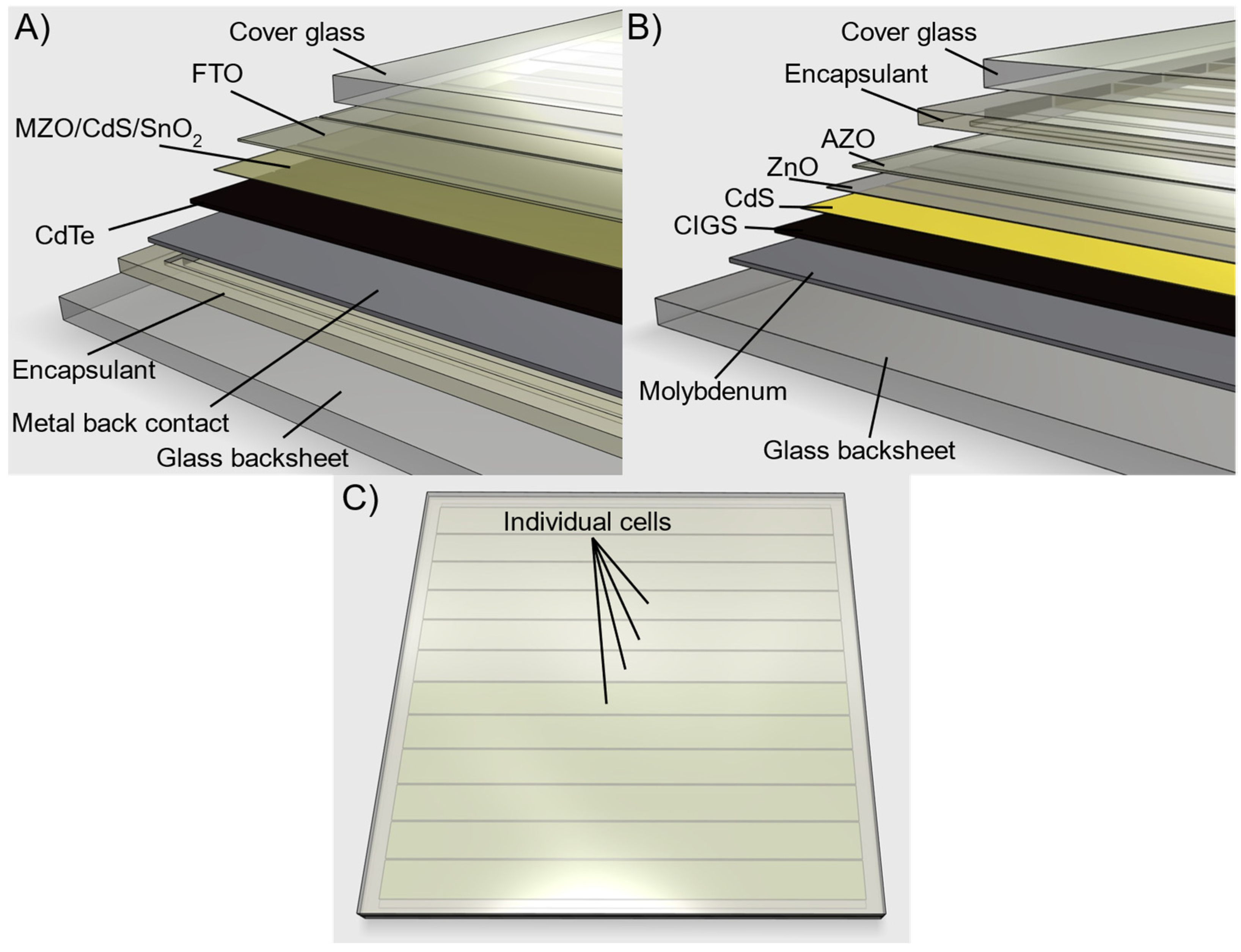
Publisher’s Note: MDPI stays neutral with regard to jurisdictional claims in published maps and institutional affiliations. |
© 2022 by the author. Licensee MDPI, Basel, Switzerland. This article is an open access article distributed under the terms and conditions of the Creative Commons Attribution (CC BY) license (https://creativecommons.org/licenses/by/4.0/).