1. Introduction
Multilevel inverters (MLIs) have become more popular with renewable energy (RE) conversion systems due to the high-quality output waveforms that are generally used in industrial applications. The attractive function of MLIs are their ability to generate a nearly sinusoidal voltage output waveform, where the stress of dv/dt is low; this enables a reduction in the loss of power, and a reduction in the total harmonics distortion [
1,
2].
Due to the scarcity of the fossil fuel-derived energy that has been conventionally used and the environmental problems it creates [
3], researchers are looking to discover novel technology, innovative uses of renewable energy, and other efficient methods to reduce emissions [
4,
5]. PV energy is the most popular and easily interfaces with recently developed MLI topologies. Presently, the total PV energy production has constantly increased by 20 to 25% each year over the last 20 years. The output voltage of the PV system is very low, and voltage changes occur alongside changes in the environmental conditions [
6,
7]. Hence, the MPPT-based technique is used with a DC–DC boost converter to generate the most power possible from PV systems. In the present literature, numerous maximum power point tracking (MPPT) techniques have been introduced to track the maximum power points (MPPs) of PV systems. The predictable perturbation and observation (P&O) control MPPT is very popular due to its simple configuration and easy execution [
3]. The problem with the P&O MPPT is that this is an iterative technique, and operational points are perturbed at regular intervals, causingoscillation around the point dP/dV = 0, i.e., the MPP. On the other hand, incremental conductance (IC) MPPT has been used to improve the tracking accuracy with dynamic performance when environmental conditions change quickly. The negatives to this process are identifying when MPPT is near the MPP and then stopping the procedure of disquieting. Hence, the working position of tracking is quickly reduced, and increased irradiance conditions occur with superior precision. Thus, in this study, a fuzzy logic controller-based (FLC) MPPT technique is used for the PV system. In this technique, the current and voltage input of PV are considered as an input, and the corresponding duty cycle is determined as the output [
3]. FLC is applied to an MPPT controller to improve the energy conversion efficiency of the DC–DC boost. The converter improves the output voltage in the form of direct current (DC); therefore, it needs to be converted into an alternating current (AC) because most of the load is in the form of an AC load. Hence, the use of the inverter converts the power from AC to DC.
Numerous MLI structures have been initiated and evaluated in various studies in the literature for the conversion of DC to AC power. MLIs were initially established around 30 years ago, but they have emerged as the preferred option, mainly for low- and medium-power appliances [
8,
9,
10,
11,
12,
13,
14,
15,
16,
17,
18,
19,
20]. In the application of solar PV systems and of wind energy conversion in particular, which enables an uninterruptible supply of power with an AC motor drive system, MLIs have been the focus of investigators. Traditional MLIs are subdivided into three categories: neutral clamped inverters (NCIs), flying capacitor inverters (FCIs), and cascade H-Bridge multilevel inverters (CHB MLIs) [
21,
22,
23,
24,
25,
26,
27]. Furthermore, traditional MLIs have some limits, such as the balancing of the capacitor voltage in NCI and FCI [
28,
29]. The CHB MLI is superior among these inverters but needs more semiconductor devices and a number of DC sources when the voltage level is increased [
30,
31,
32,
33,
34,
35]. In [
16], three H- Bridges are interconnected using two switches with bidirectional voltage-blocking capabilities. Among the three H-Bridges, only one H-Bridge is supplied with DC supply, and the other two H-Bridges are equipped with switched capacitors. The charging processes of these capacitors are enabled using interconnected switches. The authors of [
17] attained a boosted voltage via the interconnection of a non-isolated buck-boost converter and an inverter by using two capacitors. In [
18], the authors discuss a new topology with a smaller number of devices with low-stress voltage on the switching devices in order to attain a voltage of 3. The investigators in [
19] discuss a triple gain seven-level topology using a single DC supply with a high blocking voltage of 2Vdc for the switches; this topology structure has an inherent negative level of voltage production without the requirement of an H-Bridge. In [
23], a (2N − 1)-level MLI is discussed; it consists of three main parts, such as a front boost converter, one switching cell, and a two−level voltage source inverter. In [
24], the authors discuss a full bridge inverter and a three-level T-type arrangement in order to produce a seven-level output voltage, but the number of devices is very high.
All the above articles discuss producing a seven-level voltage output with a gain value of three. There are several topologies in the literature with a seven-level output voltage, but they only have a boosting ratio of 1:1.5. In [
26], the authors discuss a new topology without an H-Bridge, hence the greatly reduced TVS of this topology. In [
28], the authors discuss a generalized topology created via the arrangement of one T-type entity and a number of crisscross capacitor units. In [
29], the authors discuss a generalized MLI that was fashioned by using more SC circuits andconsisted of two switches, one diode, and one capacitor; however, it had a boosting ratio of only 1:1.5.
All of these topology configurations are based on the switched-capacitor concept, and there is no need for any sensor circuit to be able to self-balance the voltage across the capacitors. All of these these topology configurations require a significant number of semiconductor devices.
Considering the above problems of traditional MLIs, investigators have completed extensive research and developed various MLI structures using fewer devices. In this paper, a switched-capacitor-based MLI structure is developed using fewer switches, diodes, and capacitors. The proposed topology can be used alongside PV systems for low- and medium-voltage applications. The proposed structure of the PV−SCMLI topology generates a greater number of voltage levels with a high gain using only one DC source (PV source). This structure is suitable for both symmetrical and asymmetrical input sources.
Furthermore, nowadays, a significant challenge for MLIs is obtaining the optimal power and an enhanced efficiency by decreasing the THD value and the switching loss [
36,
37,
38,
39,
40,
41,
42]. Calculating the optimal switching pulses of MLIs is also a major challenge nowadays. There are two basic types of strategy used to calculate the switching pulse; one is fundamental-low-frequency switching, which performs better than the other higher frequency switching method. Predictable pulse width modulation (PWM) techniques, such as the sinusoidal PWM and space vector methods, are high-frequency switching methods that provide a quick transient reply. Different carrier-based and carrier-less PWM methods that efficiently decrease the distortion with a low EMI have been introduced. Low-pass filters can be suppressed using higher order harmonics and can improve the efficiency of MLIs.
Furthermore, lower order harmonics, suchas 3rd, 5th, and 7th order harmonics, are dominant and impossible to eradicate using the PWM method. The selected harmonic elimination (SHE) approach is thus used to calculate the optimal value of the switching angles in order to reduce the specific lower order harmonics by solving transcendental non-linear equations [
41]. In the literature, many optimization techniques are used to reduce the THD, such as particle swarm optimization (PSO), the harmony search technique (HST), and the genetic algorithm (GA). PSO is also appropriate for solving the non-linear transcendental equation when aiming to use less parameter tuning. However, PSO requires memory for the process of updating the velocity and suffers from early convergence in the primary stages. The GA algorithm convergence rate is slow and therefore does not find an optimal solution. This paper presents a novel PSO approach, i.e., anti-predatory particle swarm optimization (APSO), to solve the non-linear transcendental equations of 7L−PV−SCMLI. In the conventional PSO, a particle (bird) hunts the globally optimal result using three different behaviors, namely cognitive, social, and inertial. The cognitive and social behaviors are the components of the foraging action, which facilitate the swarm of birds to locate food. Another movement observed in birds is their anti-predatory behaviour. This helps the multitude to escape from predators [
15]. In this work, the switching angles are calculated using the APSO technique andthis estimated value of the PV-based 7L−PV−SCMLI configuration is applied in order to reduce the THD. The proposed topology features only one diode and eight switches, which are used to generate seven-level voltages and to self-balance the voltage; among the eight, only two switches are involved in the charging and discharging process of the capacitor, via which the conduction loss is reduced. Furthermore, the proposed inverter topology structure is appropriate for symmetrical and asymmetrical input sources.
The remaining structure of this paper is as follows. In
Section 1 introduces the presented work with some of the topologies conventionally used.
Section 2 describes the modeling of the PV cell.
Section 3 describes the configuration of the DC–DC boost converter employed to produce the optimal power using the PV system.
Section 4 discusses the Fuzzy MPPT technique used to make the duty cycle of the converter.
Section 5 discusses the proposed 7L−PV−SCMLI topology and the switching scheme of the inverter. The generalized proposed structure is presented in
Section 6.
Section 7 discusses the calculation of the switching angles using the APSO algorithm and compares it with the GA. In
Section 8, the proposed topology is compared with the recently developed MLI topologies.
Section 9 presents the verification of the results and simulation of the proposed 7L−PV−SCMLI configuration.
Section 10 presents the conclusion to the work discussed.
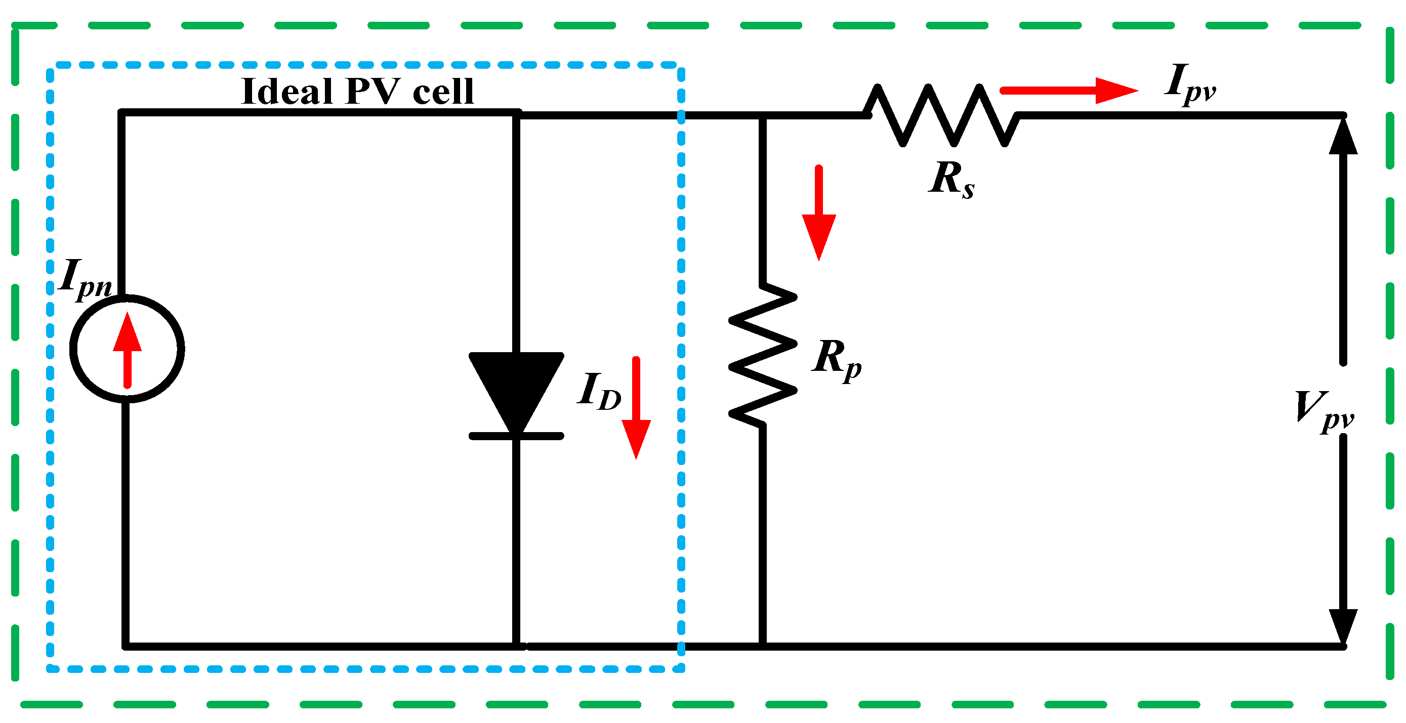
2. Modeling of PV Cell
The configuration of a PV cell is represented in
Figure 1. In the PV system, the PV cells are connected in series and in parallel. In the production of energy, the collision of electrons with photons enables the cells to reach superior energy levels, and electrons turn free in order to travel across junctions and thus generate current [
3,
5]. The photocurrent
Ipv that is generated by PV cells is reliant on the solar illumination level.
With the help of Kirchhoff’s current law from
Figure 1, the equation used to calculate the current output of the PV cell (
Ipv) can be described as follows:
The production of current by photons (
Ipn) is equal to the solar irradiation,
ID defines the diode current, and
Ish describes the shunt resistor current. The characteristics of the PV module equation are represented as follows:
where the saturation current is represented by
Io, the voltage of the PV module is represented by
Vpv,
Rs and
Rsh define the series and shunt resistance,
Cs and
Cp are defined as the total number of cells in series and in parallel,
q defines the charge of the electrons,
Z defines the identity factor of the diode, and
K and
Tm define the Boltzmann constant and the temperature of the cell.
Ipn and
Io are represented in Equations (4) and (5), respectively, as follows:
where
Itsc defines the standard test short circuit current of the PV module for conduction at the standard test conditions (STC) of 25 °C and 1000 W/m
2,
Ki defines the coefficient temperature of the short circuit current,
Tr defines the temperature reference value in Kelvin,
S defines the solar irradiation,
Sr defines the solar irradiation reference,
Isc defines the value of the saturated current at 25 °C, and
Ego defines the band gap.
4. Fuzzy MPPT Algorithms
The FLC MPPT technique is used in this work to obtain the enhanced performance of the MPPs. The response of the FLC MPPT technique is fast and improves the system performance when attaining the MPPs [
3]. The working steps of the FLC MPP processes depend on the heuristic rule and lead to an adaptive stepwise that is sensorless with respect to sunrays. In addition, the convergence is quicker among the temperature changes.
Figure 3 signifies the fundamental model of the FLC MPPT technique.
The input data applied to the FLC MPPT generally include error E and the change in error ΔE. The processes of the FLC are made with three functional blocks, i.e., fuzzification, the algorithm rule of the FLC, and defuzzification. A description of all the three main functional blocks is presented below:
Fuzzification: In terms of the fuzzy set with a linguistic level, the FLC MPPT technique requires input variables. The actual voltage of the PV array is determined by using the voltage (
V) and current (
I) to calculate the power. In this process, two input variables are used to control the performance, i.e., error
E and the change in error (
CE), at the time of sampling, which is (
Z). A detailed explanation of
E and
CE is given in Equations (7) and (8), as follows [
3]:
Here,
P(
Z) and
V(
Z) indicate the output power and the voltage of the PV module, respectively. With the help of fuzzification, the input variables of
Figure 4a,b, and the output obtained in
Figure 4c, are compared with the pre-defined target value using the fuzzy toolbox. When
Z of the input
E(
Z) operates at the point located on the left side or the right side of the MPP of the P–V characteristic, then the input error
CE(
Z) expresses the direct dislocation of the working point. Using a DC−DC converter improved the
D as the output of the proposed controller. Subsequently, according to slope
E(
Z), by changing the duty ratio, the control point is brought to the reverse of the point at which the slope is zero.
Algorithm Rules (Inference Engine): The inference engine works based on the fuzzy rules and fuzzy inference sub-block. In this process, the fuzzified inputs allow the interface engine to apply fuzzy rules. In this work, five linguistic variables are considered, i.e., big negative (BN), small negative (SN), zero (ZE), small positive (SP) and big positive (BP); this is performed using the MATLAB/Simulink platform in the fuzzy toolbox. The input and output variables of the fuzzy membership function that are based on the five subsets of the membership functions are represented in
Figure 4.
Table 1 shows the fuzzy associative control memory, while error (
E) is the matrix entry of the fuzzy sets, and the change in error (
CE) and change in the duty cycle ratio are delta-
D of the converter.
In this paper, the fuzzy method is performed using the Mamdani inference scheme. This is applied using the max–min interface method of fuzzy arrangement. The three-dimensional (3D) appearance of the twenty five FLC rules on the surface of the MPPT is represented in
Figure 5 in a graphical shape.
Figure 5 shows the duty cycle variation concerning error (
E) and the change in error (
CE). These also verify the suitable function of the fuzzy controller.
5. Proposed 7L PV-SCMLI
The proposed topology uses fewer devices, and it can self-balance the voltage of the capacitors. The configuration of the proposed topology is simple and can be easily extended to produce superior voltage levels. The proposed 7L−PV−SCMLI topology has eight IGBT switches, two capacitors, and one diode. Out of the eight switches, only two semiconductor switches are active in the capacitor charging path processes, reducing the conduction loss. This topology sees an gain of three via the use of only a single PV DC source. To produce the 7L voltage, only four switches conduct at a fundamental frequency, reducing the switching loss and improving the performance. Switches
SW1 and
SW4 have reverse voltage-blocking capabilities. The PV source charges both capacitors
C1 and
C2 separately, linking them in parallel with the PV system, and it discharges in series through the DC source to load the high-voltage level. This topology generates the voltage levels +
Vdc, +2
Vdc, +3
Vdc, 0, −
Vdc, −2
Vdc and −3
Vdc. Hence, the gain of the topology is three. To avoid a short circuit, two sets of complementary switches,
SW5,
SW6, and
S7 and
S8, are used. The H-Bridge switches,
SW5 and
SW8, have an maximum blocking voltage (MBV) of 3
Vdc, switches
SW2 and
SW3 with a diode have an MBV of 2
Vdc, and switches
SW1 and
SW4 have an MBV of
Vdc. The switching signals of the proposed 7L−PV−SCMLI topology are represented in
Table 2. The proposed structure of 7L−PV−SCMLI is shown in
Figure 6a, and the corresponding voltage waveform pattern is shown in
Figure 6b.
Figure 6b shows that the magnitude of the voltage levels is unequal due to the input of the proposed inverter when a renewable PV source is considered.
In this work, the initial voltage level magnitudes are unequal due to the renewable energy sources used.
Figure 6b shows the unequal magnitudes of the voltage levels. The total voltage output of the MLI is specified by V =
Vdc + 2
Vdc + 3
Vdc.
Operation Modes of 7L−PV−SCMLI
The different modes of operation for the proposed inverter are shown in
Figure 7. In
Figure 7, the red colour indicates the resistive lane used to generate the levels of voltage and the light green colour represents the charging lane.
Mode 1 (0Vdc): In this mode, the voltage level is obtained via the redundancy of two switches, either by turning on switches
SW6 and
SW8, or by turning on switches
SW5 and
SW7, as represented in
Figure 7a. At this level, capacitor
C1 can be charged in this mode by switching on
SW2; at this stage,
C2 is in floating mode.
Mode II (+Vdc): Switches
SW5 and
SW8 are turned on in this mode and the +
Vdc level of voltage is obtained, as shown in
Figure 7b. However, the SW
2 capacitor
C1 is charged and
C2 is in floating mode.
Mode III (+2Vdc): Switches
SW1,
SW5 and
SW8 are switched on to generate the +2
Vdc voltage level, as shown in
Figure 7c. Meanwhile, load capacitor
C1 is discharged and
C2 is charged with
Vdc by turning on the switch
SW4. In this mode, the diode works as a reversed bias owing to the voltage across
C1.
Mode IV (+3Vdc): The +3Vdc level of voltage is obtained when switches
SW3,
SW5 and
SW8 are turned on, as shown in
Figure 7d. Both capacitor
C1 and
C2 are discharged via the load. In addition, the diode gets reverse biased in this mode by the total voltage across the
C1 and
C2.
Mode V (−
3Vdc): Capacitors
C1 and
C2 are both in the discharging mode series with the source, as shown in
Figure 7g. In this condition, the voltage stress across the diode is 2
Vdc.
Mode VI (−
2Vdc): This mode is generated by the PV supply voltage and the voltage across the
C1. Switches
SW1,
SW6 and
SW7 switch on in this mode, as shown in
Figure 7f.
Mode VII (−
Vdc): This mode is obtained by switching on
SW6 and
SW7, as shown in
Figure 7e. Capacitor
C1 is charging in this mode,
SW2 is the same and
C2 is in floating mode.
7. Switching Angles Calculation
A new version of the PSO variant with an anti-predatory activity, proposed by Selvakumar and Thanshkodi, is named Anti-predatory Particle Swarm Optimization (APSO) [
15]. The activity of the anti-predatory method works based on the phenomenon of bird flocking. The swarm or particle (bird) dodges its predators during this process. The working action of APSO is separated into two different components: (a) Cognitive behavior is divided into a good-quality knowledge component and a bad experience component. (b) Social behavior is divided into an excellent global experience component and a global worst experience component. The superior knowledge component of a swarm represents the memory of the earlier allotted best location, whereas the bad experience component indicates its earlier visited worst location. In this paper, the worst position points are predators, whereas food locations are modeled using the position of the best points in standard PSO.
The new and modified position-velocity update equation in the APSO system is modified according to Equations (9) and (10), as follows:
7.1. APSO Algorithm for THD Calculation
Step 1. Initiate the modulation index (MI) term, population size, number of maximum iterations (itermax) and coefficients of acceleration, i.e.,, , and . ; values lying within the range of 0.1 to 2 and and are in position 2. Randomly make a set of switching angles, i.e., α1, α2 and α3.
Step 2. The values of the switching angles should satisfy the practicability criteria lying in between [0, 90], i.e., 0< αi < 90 for I = 1, 2, 3.
Step 3. Using the formula, the feasibility of the particle is checked using the formula below:
where
g(
x) and
h(
x) are the dissimilarity and similar constraints, respectively.
If = 1, x is feasible and if > 1, x is infeasible.
Step 4. The fitness function f(x) for every set of switching angles is determined.
Step 5. If the calculation value is feasible as it is, then the value is considered otherwise, and the improvement factor is added as a function. The correction factor is |(C1*N + C2*S(x))|; here, S(x) denotes the summary of all constraints, C1 and C2 are correction coefficients, and N denotes the number of constraints.
Step 6. The starting positions of the swarms until iteration r are measured as the best local location of the particle, i.e., , and best global location , are the fitness function f(x) of the minimum value. Correspondingly, the closing location of the swarms are taken as the worst local position, i.e., , and the location of the global worst , are the highest values of the fitness function f(x).
Step 7. The position and velocity of the particle are modified by Equations (9) and (10). Finally, the best location of the swarms is calculated by comparing the new location of the swarm population with the original location of the particles in swarms and modifying the iteration count.
Step 8. When the iteration count attains the highest set value, then the fitness function is calculated by changing the modulation index from 0.1 to 0.9.
Step 9. Otherwise, repeat Steps 4 to 7.
The working processes of the APSO algorithm flow chart pattern are shown in
Figure 9.
7.2. Comparison of GA with Proposed APSO Algorithm
The behavior of both the GA and APSO algorithms are compared, and it is observed that both algorithms converge with acceptable solutions at all modulation indexes (MIs). Firstly, both algorithms converge at a MI of 0.9 with a population size of 100 individuals. The GA could find the objective function of 11.7651% in 200 generations, while the APSO algorithm converged to a better solution of 10.1124 in 50 iterations. Similarly, in the convergence of both the GA and APSO algorithms at a MI of 0.9 and 100 individuals, the GA gives the objective function of 3.9531. At the same time, the APSO converged at the same MI of 0.9, demonstrating a better solution of 2.6541 in 250 iterations. This result shows that APSO has a faster convergence than the GA.
A comparison of the behavior of the GA and APSO algorithms is shown in
Table 3. From the compared values, it is observed that both algorithms converge with satisfactory solutions at all modulation indexes.
Table 3 shows the details of the best objective with the corresponding computation times of 50, 100, and 250 iterations. With 100 individuals per population, both algorithms run 25 times at modulation indexes of 0.5, 0.7, and 0.9. Moreover, for the robustness verification of both algorithms, a test is performed using the MATLAB/Simulink platform on an Intel(R) core (TM), i5, 2.60 GHz processor, taking the computational time and the ability to achieve the objective value into consideration when all other conditions are kept unchanged. Comparative results under the same condition show that the APSO algorithm always converges faster than the GA, giving APSO a better solution.
Figure 10a shows the variation in the switching angles obtained using APSO for different MI. The switching angles satisfy the following conditions:
. The THD obtained using both the algorithms (APSO and GA) against the MI is plotted in
Figure 10b, taking a population size of 100 individuals. A lesser THD is obtained with a full range of MI when using APSO compared to GA. This also signifies that theAPSO algorithm converges to a better solution than the GA. The THD decreases with an increase in MI, which satisfies the operational principle of MLIs.
8. Proposed Topology Comparisons with Other Topology
The proposed 7L−PV−SCMLI topology is evaluated using the exisitng seven-level topologies previously published in the recent literature. A comparison of different types of data regarding MLI topologies is shown in
Table 2. In the comparative analysis conducted in this paper, the number of switches, the diodes in the series–parallel combination, the number of DC sources, the number of capacitors, the number of driver circuits, the gain, TVS, MBV and the cost factor (
CF) are considered. To calculate the cost factor used, the formula is as follows:
here,
NSW, ND, NC and
NDR indicate the number of switches, number of diodes, number of capacitors and number of driver circuits.
a indicates the weight factor and its value depends upon the weight given to the switching device and TVS
p.u. When
β > 1, more weight is given to TVS
p.u. If the value of
β < 1, more weight is given to the switching devices. In this paper, equal weight is given to both the switching devices and TVS
p.u, therefore
β is considered as 1. In [
21], the number of switches and driver circuits is fewer compared to the proposed topology, but the gain value is only 1.5. The study of [
25] uses only one capacitor less than the proposed technique. However, the value of gain is 1.5. Furthermore, in this topology, four switches are in the charging circuit, while in the proposed topology, only two switches are in the charging circuit.
Table 4 represents the comparison of the proposed topology with different seven-level topologies.
Figure 11a compares the number of switches with the number of voltage levels, and
Figure 11b corresponds to the
Gc coefficient variation regarding the levels of voltage output.
Figure 11a shows that the CHB MLI, DC MLI and FC MLI switching device requirements are greater when the number of levels increases more than the proposed SC MLI topology. Furthermore, in the construction of the CHB MLI, the value of
Gc is high compared to the conventional MLIs, including the DC MLI and FC MLI. The SC MLI structures have a lower value for the
Gc coefficient than the CHB MLI, DC MLI and FC MLI structures. This represents the size of the MLI and the total cost for design; the SC MLI is less predictable than the previous H-bridge-based MLI structures.
9. Results and Simulation
The proposed 7L−PV−SCMLI consists of eight switches, one diode, two capacitors, and a single DC source. This configuration is simulated in a MATLAB/Simulink environment. The input of the inverter is taken as a PV source with a boost converter, and the boosted voltage output is obtained at 175 V, as shown in
Figure 12. Initially, from 0 to 0.7 s, the distortion in the output voltage is more due to changes in the irradiance and environmental condition. After 0.7 s, the PV boost converter system produces the constant output voltage, as shown in
Figure 11. The frequency output of the inverter is 50 Hz, and the load is considered as resistance (R) = 150 Ω and inductor (L) = 200 mH. IGBTs are taken as the switching device, and capacitors
C1 and
C2 are chosen at a 2200 µF rating based on the longest discharging period. The selected harmonic-based APSO technique discussed in
Section 7 is used to calculate the optimal firing angles while keeping the value of the THD at a minimum. The three non-linear transduction equations that are correspondingly solved by the selected harmonic elimination and calculated switching angles are used to control the performance of the inverter IGBTs switches.
Figure 13a represents the capacitor voltages Vc1 and Vc2. From
Figure 13a, it can be observed that initially, in capacitor voltage Vc1 and Vc2, there are more variations from 0 to 0.7 s because the change in the irradiance is high. For more clarification, the zoomed capacitor voltage from 0.16 to 0.24 s is represented in
Figure 13b.
Figure 13c shows the capacitor voltage from 0.7 to 1 s with an RL load. From
Figure 13c, it can be observed that both capacitor voltages (Vc1 & Vc2) give a constant output voltage from 0.7 s.
It can be observed from
Figure 13 that the capacitor across the voltage is stable at 175 V and that there are lesser variations with a low ripple in voltage.
Figure 14a shows the switching pulses at the modulation index of 0.9, and the total standing voltage (TSV) is shown in
Figure 14b.
Figure 15a represents the output voltage and current of the proposed 7L−PV−SCMLI with R-load and RL-load performance. Figure shows that from 0.16 to 0.2 s, it performed as an R-load and from 0.2 to 0.24 s, it performed as an RL-load current. Hence, this proposed inverter is suitable for both load conditions with a PV source.
Figure 15b shows the overall proposed multilevel inverter output voltage in which the observed initial distortion in the voltage is more in which after 0.2 s, the voltage is stable with an optimal output.
Figure 16a shows the fast fourier transform (FFT) analysis of %THD for the 7L−PV−SCMLI voltage output waveform. In
Figure 16a, the value of %THD is 11.9% when the modulation index is 0.1.
Figure 16b shows that the %THD value is 5.68% when the modulation index is 0.9. It can be clearly observed from
Figure 16 that when the modulation index range changes from 0.1 to 0.9, then the % value of the THD is reduced.

 ,
, 


