Article

Comparative Study of Different Perovskite Active Layers for Attaining Higher Efficiency Solar Cells: Numerical Simulation Approach

1
Technology Innovation and Development Foundation, Indian Institute of Technology Guwahati, Guwahati 781039, India
2
Department of Physics, Arunachal University of Studies, Namsai 792103, India
3
College of Engineering, University of Warith Al-Anbiyaa, Karbala 56001, Iraq
4
VLSI Centre of Excellence, Chitkara University Institute of Engineering and Technology, Chitkara University, Punjab 140401, India
5
Department of Electrical Engineering, University of El Oued, El Oued 39000, Algeria
6
Department of Chemistry, College of Sciences, King Khalid University, Abha P.O. Box 9004, Saudi Arabia
7
Institute of Electronics, Atomic Energy Research Establishment, Bangladesh Atomic Energy Commission, Dhaka 1349, Bangladesh
8
Department of Advanced Energy Engineering Science, Interdisciplinary Graduate School of Engineering Sciences, Kyushu University, Fukuoka 816-8580, Japan
*
Author to whom correspondence should be addressed.
Sustainability 2023, 15(17), 12805; https://doi.org/10.3390/su151712805
Submission received: 16 July 2023 / Revised: 17 August 2023 / Accepted: 21 August 2023 / Published: 24 August 2023

Abstract

:
The simulated device structures of ITO/ZnO/Perovskite absorber layers (PAL)/Spiro-OMeTAD/Au with distinct absorbers were modeled and investigated using solar cell capacitance simulator (SCAPS-1D) simulating software (version 3.8). The primary objective is to enhance the thermal stability of the solar device. As the absorber thickness and temperature impact PV performance parameters, thus main aim of this work is to determine the optimum thickness of PAL as well as the temperature affectability on the PV performance of the cells. It was also observed that the maximum PV parameters (among the cells under consideration), viz. 29% PCE, are achieved with the formamidinium tin iodide (FASnI3) at the thickness of 600 nm. Similarly, the temperature of 300 K shows a much-improved efficiency offering nearly 29%. Further, the external quantum efficiency (EQE) and J-V also confirm the determent of the more stable, lead-free, FASnI3-based device, which can provide an effective way to develop highly efficient, low-cost solar cell devices.

1. Introduction

Since the last decade, technical development in organic–inorganic solar cells has revolutionized the hunt for a better replacement for currently available energy resources [1]. Due to the superior results, the community of researchers has predominantly expanded in energy sources. It has taken a lot of work, but better power conversion efficiency (PCE) at significantly lower manufacturing costs is the outcome [2,3]. In addition, the perovskite (PVK)-based solar cells [4,5,6,7,8,9,10,11,12,13] have drawn interest from researchers due to their intrinsic qualities, such as improved carrier mobilities, extended carrier diffusion lengths, and a much simpler and more efficient production procedure [14,15,16,17,18].
However, Kojima et al.’s pioneering reported PCE up to 3.81% and 3.13% utilizing iodine (I) and bromine (Br) as the halide materials that were reported in 2009, which were the continuation of his first research efforts of the initial research work of the perovskite solar cell [19,20]. It is also interesting to note that the light-absorbing material of Methylammonium Lead Triiodide (MAPbI3) allowed for a significantly enhanced efficiency of up to 22.1% in less than ten years [21,22]. Similar to the context, a certain number of prior research showed that a PVK material based on the MAPbI3 with the chemical composition of PQX3 might reach a much-enhanced efficiency, where P is the methylammonium cation (MA+ or CH3NH3+), Q is used as the Pb, while X presents the anionic halides, respectively. Although the MAPbI3 active material still offers significantly greater efficiency, its environmental toxicity and the Pb materials instability in the PVK material are the main causes of worry since they might impede commercial manufacturing [23,24]. Previous works by Azri also showed a higher value of PCE with the PSC design up to 25.02%, which is one of the most exclusive simulative studies [25]. Another work by Raoui improved further up to 26.74% using the diverse charge selective contacts [26]. But the volatility nature of MA cation in the MAPbI3 always remains a problem for these types of PSC.
An alternative Pb material may be used to consider ecological benefits in order to overcome these obstacles. A far superior germanium (Ge) competitor may be employed as the perovskite material due to higher stability and environmental friendliness, yet offering equal optoelectronic properties on the device [27]. Additionally, better stability may be attained using the MAGeI3 active layer as opposed to MAPbI3 for Ge, which is less degradable as compared to the Pb material. Additionally, the Ge material is excellent for the production of PSC devices because of its improved stability at high temperatures up to 150 °C. For this reason, the current study uses a computational simulation of a PSC based on Pb-free material of methylammonium germanium-iodide (MAGeI3). Previous work also has shown the promising applications of germanium-based two-dimensional materials for solar cell applications [28]. Also, the detailed study and the analysis of Transparent Electrodes and Active Layers are shown in the recent work by Guo et al. [29].
Similarly, the FA-based PSC is always suitable for the design and manufacturing of the PSC for the more stable nature of the perovskite [30]. The FASnI3-based PSCs are lead-free and stable alternatives for suitable optoelectrical parameters. The previous works in the FASnI3-based PSC are explored for a better understanding of the importance as well as the current state of perovskite solar cell technology. It is noted that the interface engineering for enhanced efficiency and stability was highlighted by Meng et al. [30]. Efficient hole extraction utilizing Spiro-OMeTAD was explored by Kayesh et al. [31], while Gu et al. [32] investigated carrier transport mechanisms. Record-breaking efficiencies and defect passivation strategies were underscored by Meng et al. [33] and Zillner et al. [34]. Low-temperature solution processing was emphasized by Liu et al. [35], collectively advancing FASnI3 PSCs as promising candidates, progressing in efficiency, stability, and fabrication techniques.
The basic phenomena present in photovoltaic (PV) devices are described and made simple by the simulative approach, which identifies the influence of the key factors in achieving the optimal device output. It should be highlighted that developing a solar cell without using a numerical modeling technique is impracticable from the standpoint of increased costs and time. The method reduces risk, analyzes the qualities of the basic layers, and offers a thorough investigation into improving the performance outputs of the PSC [36]. Additionally, utilizing real-world examples from PSC, the technique offers a practical way to assess the importance of various material properties. Numerical simulation also becomes essential, particularly in material science [37]. It advances, further projecting the fastest route for discovering novel functional materials that provide insight into future research [38,39,40,41,42] and makes important suggestions about the existing material features. Despite the numerous benefits of numerical techniques in producing observed effects qualitatively, there is still some debate about them, particularly regarding the error-prone parameter extraction due to the relation of the modeling parameters, incorrect extraction of the parameters, and successive unique determination [43]. Simultaneously, the exclusive numerical simulation process is complex and challenging in assigning device performances. Numerical simulation can also be quite expensive due to memory constraints and lengthy calculation times, particularly for defect-related phenomena [44]. Due to the inaccuracies caused by the supercell’s finite size, huge supercells are implemented in the simulations to verify the accuracy of the defect formation energy (charged) [45]. Additionally, the numerical simulation fails to solve multi-dimensional issues, and it might be challenging to comprehend the results [46]. The values ascribed to the physical model parameter values significantly impact the outcomes of the numerical simulations. As a result, it has to be precisely calibrated to provide the intended outcome. A mismatching value between the calculated and experimental data is produced by even a little variable inaccuracy.
Certain numerical simulations can need pricey software (SCAPS 3.8) to obtain the device’s features as well. The one-dimension SCAPS-1D, designed and developed by ELIS, University of Gent, Belgium, and operating on the drift-diffusion model, is a superior numerical simulator that is used to test the device performance in order to eliminate all of these repercussions [47,48,49,50,51,52]. The present simulator offers a special set of benefits, including the option to practically grade all the parameters and the capacity to deposit up to seven semiconductor layers [40,48,49,53]. The simulations may be run in both dark and light environments, and its operating principle is based on resolving the Poisson and the continuity equations [40,53]. In addition, the aforementioned simulator makes it simple to simulate diverse models with recombination mechanisms, batch calculations using bulk, and the computation of interface defect levels [54]. Both crystalline and amorphous solar cells can use the current simulation [55]. In addition to the SCAPS-1D simulator, modeling solar cell devices may also be done using other simulating programs such as AFORS-HET, TCAD, Silvaco ATLAS, and Lumerical. However, device optimization is not available in all sorts of solar cells in PV solar cells due to a few limitations and insufficient methods in physical models and parameters [56,57,58,59,60,61,62,63]. However, the main issue with the SCAPS-1D is the struggle to solve multi-dimensional issues, and it is also difficult to comprehend the findings in detail.
Suitable carrier transport layers (CTLs), in addition to the simulator, are required to maximize device efficiency, according to the PSC’s ongoing improvement. However, TiO2 materials’ shortcomings as an ETL result from insufficiently high carrier mobility and a detrimental impact on device stability under UV irradiation. Therefore, choosing ETL is necessary to provide higher electron transmission across the PSC device. As a result, increased carrier counts are to be anticipated when ETL material is optimized, as the more significant bandgap alignment and carrier mobilities result in much higher solar cell outputs. Initially, high PCE was optimized by TiO2 in ETL since it showed a higher value of 24.23% [64]. In the meantime, an optimized PCE up to 21.36% has been found utilizing stable ZnO as ETL in Pb-based PSC, according to prior results by Liu et al. [65]. Similarly to this, several HTL materials are evaluated to ensure good efficiency for the transmission of the holes. According to earlier publications, a remarkable PCE is accomplished by employing Spiro-OMeTAD, which is stable as well as has a higher value of carrier mobility [66]. Therefore, it is necessary to maintain the superior hole transmission throughout the PSC. Additionally, it is also necessary to mention that the finest combination of both the HTLs and ETLs is to be sustained for improvement in the efficiency of the PSC device. The PSC’s efficiency may be greatly increased thanks to the improved band alignment and high carrier mobility of these materials [67].
In the current report, the exclusive investigation of the influence of various absorber materials such as MAPbI3, methylammonium tin iodide (MASnI3), methylammonium germanium iodide (MAGeI3), and FASnI3-based PSC designs under the AM1.5 illumination is completed. The absorber thickness must also be tuned in order to maximize efficiency for the PSC’s unique device construction. Additionally, the improvement in PV characteristics for a better PSC device, suitable CTL of ZnO and Spiro-OMeTAD are utilized for the simulated PSC and have a discernible EQE parameter. The detailed analysis of defect density, temperature dependency, EQE, and JV curves is also analyzed and investigated. The investigation is organized as follows: Section 2 depicts PSC device architectures with simulation settings; Section 3 explains mathematical modeling with findings and discussions in Section 4; and the conclusion is in Section 5.

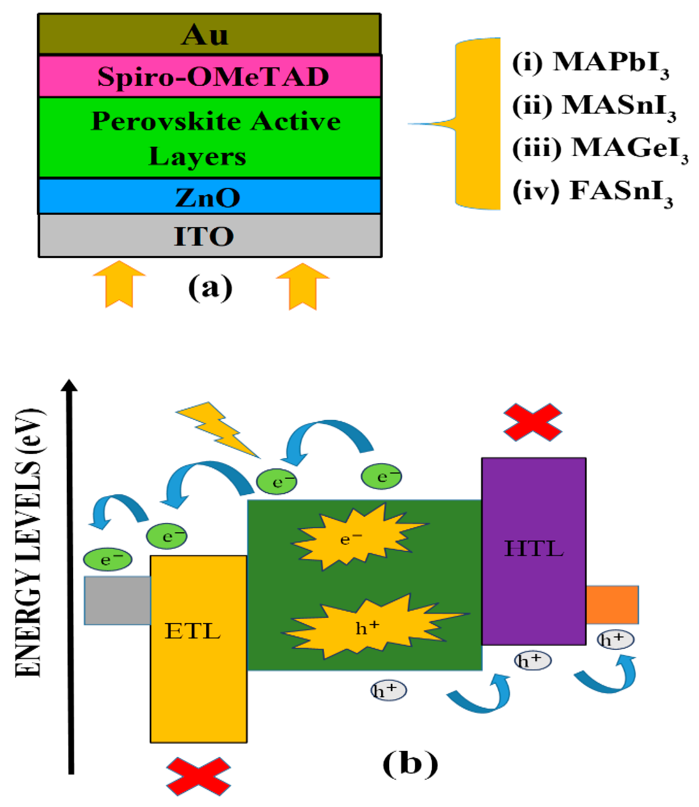
2. Device Structure and Optimization Methodology

The design of the configuration for the computational approaches of the PSC and working principle is schematically represented in Figure 1, where four types of perovskite absorber layers are used. The basic construction in the PSC is made with three distinctive layers; firstly, one perovskite absorbing layer (PAL) is sandwiched between the electron transporting layer (ETL) and the hole transporting layer (HTL). Similarly, the HTL is associated with the metal back contact (i.e., Au), while the ETL is associated with the transparent indium tin oxide (ITO), as presented in Figure 1a. Here, the absorber layers are MAPbI3, MASnI3, MAGeI3, and FASnI3 materials layer as the PAL with a 200 nm thickness. The FASnI3 materials have a bandgap of 1.41 eV, so a wider range of photon wavelength can be absorbed by the material than other perovskites of MAPbI3 and MAGeI3. The optical properties are considered by the SCAPS-1D software (version 3.8), and it effectively enhances in overall output parameter of the PSC device. It can also be illustrated that all the PSC constructions are illuminated under the incident power density of 100 mW/cm2 and the solar spectrum of AM1.5. In the simulation, Firstly, to carry out our simulations, ZnO and Spiro-OMeTAD layers are chosen for suitable HTL/ETL from earlier work by Bhattarai et al. [68]. Since Spiro-OMeTAD and ZnO can be selected for their better functioning of the PSC. Figure 1b illustrates the working principle of the designed PSC with the CB and VB values of the component layers, as the HTL will block electrons while holes will be blocked by the ETL, respectively. The simulated parameters in SCAPS-1D for the different absorber materials, ETL, and HTL are validated from previous reports, as shown in Table 1. At the same time, the details of the interface (IF) defects are depicted in Table 2.

3. Mathematical Modeling

The significant solar cell parameters that influence the outputs can easily be obtained utilizing the SCAPS-1D numerical simulator. SCAPS-1D is known as the 1-dimensional solar cell capacitance simulator, which was designed and developed by Burgelman et al. [45]. Basically, the semiconductor materials under steady-state conditions are governed by the one-dimensional equation. The dependency between the electric fields (E) and the charge density ( ρ ) for the p-n junction can be symbolized using the following equations:
2 φ 2 x = E x = ρ ε s = q ε s p n + N D + ( x ) N A ( x ) ±   N d e f x
Here, the electrostatic potential is  φ , whereas the charge is  q , and the static relative permittivity of the medium is  ε s , the electrons and the hole are n and  p , respectively; while the density of the donor and acceptor are presented by  N D + N A + , and the defect density of the acceptor and donor is represented by  N d e f x .
The carrier continuity equation in the PSC device can be represented as follows:
j p x + G U p n , p = 0
j n x + G U n n , p = 0
where the electron and hole current densities are  j n  and  j p , the carrier generation rate is presented by  G  and the recombination rate of electron and hole is represented by  U n n , p U p n , p , respectively.
Similarly, the current density of the carriers can be obtained from the following equations [39]
j p = q n μ p E q D p p x
j n = q n μ n E + q D n n x
Here, the charge  i s   q ,   a n d  carrier mobilities are  μ p  and  μ n , respectively, while the carriers’ diffusion coefficient of holes and electrons are  D p  and  D n .
The SCAPS-1D software (version 3.8) abstracts all the fundamental equations of the solar cells, such as the current density, generation rates, and recombination rates, respectively.

4. Results and Discussion

The section is divided into six subsections. Section 4.1 shows the study of the band energy diagram, Section 4.2 shows the influence of PAL thicknesses, Section 4.3 shows the influence of temperature on the efficiency depicted for the PSC designs, Section 4.4 illustrates the influence of the total defect density (DD) on the PCE, Section 4.5 offers the pi-diagram representation for PCE of different PSC designs, and at last, the EQE and J-V parameters are depicted in Section 4.6.

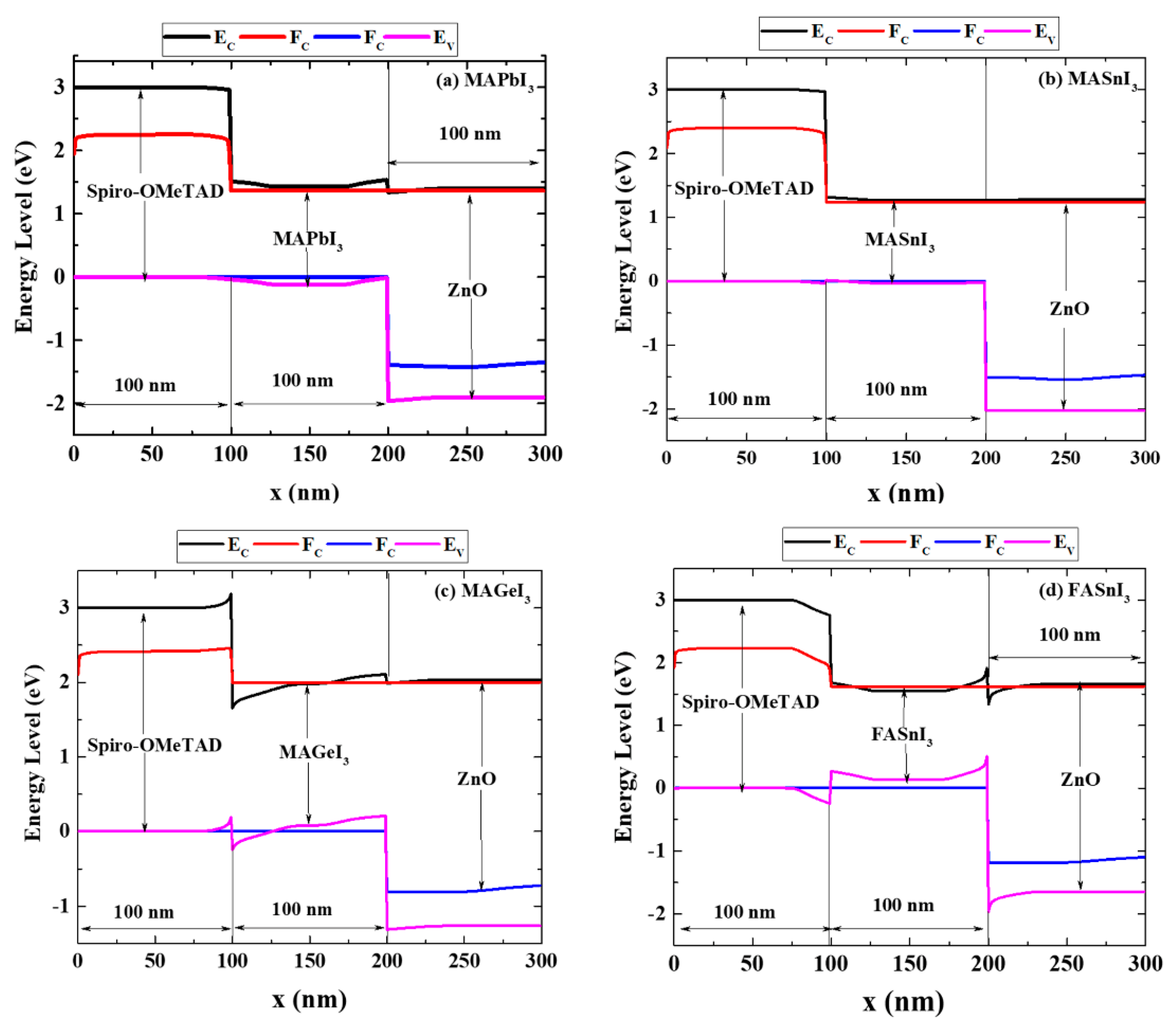
4.1. Study of Band Alignment of the PSC Devices

Band engineering is an effective way to achieve excellent efficiency for PSCs. For effective transport of the electrons from the PAL to the ETL (ZnO), the conduction band (CB) of the absorber has to be slightly above the CB of the ETL. In a similar way, the valence band (VB) of HTL(Spiro-OMeTAD) should be slightly below the VB of the HTL for effective transport of holes. The band alignment diagram of the simulated PSCs in this work, as illustrated in Figure 2, shows the electron movement from the absorber layer (FASnI3) to ETL for a barrier of 0.5 eV at 300 K. This transport of electrons arises due to the proper band alignment between the CB of perovskite and ZnO material. To attain optimized PV performances with the mentioned PSC device configurations, retaining a suitable band alignment amongst the constituent layers of the devices, including the HTL and the PAL, is essential. The transportation of holes to the HTL is confirmed via maintaining an impeccable band alignment amongst the VB of PAL and the HTL. In this study, MAPbI3 perovskite materials have a bandgap of 1.55 eV, MASnI3 has a bandgap of 1.3 eV, and MAGeI3 has a bandgap of 1.9 eV, whereas FASnI3 has a bandgap of 1.41 eV; respectively. There exists a suitable band alignment between the ETL (ZnO) and the PAL (FASnI3), and HTL (Spiro-OMeTAD), as illustrated in Figure 2. At a temperature of 300 K, the electrons can pass a barrier of 1.1 eV. Similar to how holes may be transported from the PAL to the HTL, a band alignment exists between the HTL and the PAL. The choice of the metal contact at both the front–back contacts created an intrinsic electric field that helped to maintain one throughout the device design, allowing for the easy movement of charge carriers.

4.2. Influence of PAL Thickness on the PSC Outputs

The PAL thickness is considered to be a significant parameter that contributes to optimizing the solar cell outputs. Equilibrating the generated electrons and holes from incident photons should be optimal to improve the absorbance and decrease the recombination. Figure 3 illustrates the comparison of VOC, JSC, FF, and PCE with different thicknesses of the PALs such as MAPbI3, MASnI3, MAGeI3, and FASnI3-based PSC. It is evident from Figure 3 that for the MAGeI3-based PSC device, VOC starts to decrease, while all three PSCs show an invariable value of VOC, as shown in Figure 3a. The variation in VOC mainly depends on the cell’s dark saturation current, which is a function of carrier recombination in the PSC. So, the VOC depicts the measurement of the recombination value in the PSC. As the PAL thickness increases, the perovskite material’s recombination improves as well. Hence, it shows a decrement in VOC. Also, it is necessary to mention that VOC is the function of the band gap of the absorber material. As MAGeI3-material has a higher band gap, it also shows higher VOC than the lower bandgap material of MASnI3 (1.3 eV).
While Figure 3b indicates that with increasing PAL thickness, there is an increment in current density (JSC) for all the PSCs. This suggests that bigger absorber layers may absorb more photons and create more carrier concentration at longer wavelengths, promoting the generation of electron-hole pairs. However, it is clearly visible that MASnI3 has a higher JSC than MAGeI3 due to more absorption for a higher range of photon absorption. This suggests that MASnI3 has better electron and hole production properties, which ultimately shows a higher JSC of 34.2 mA/cm2, whereas the least value of 19.5 mA/cm2 for MAGeI3-based PSC devices.
Figure 3c shows that MASnI3 and FASnI3-based PSC has a decrement in FF with increasing thickness. It is due to the reduced VOC with increasing PAL thickness which can be depicted in Figure 3a. But, at the same time, the FF of FASnI3 shows a better FF because, compared to the other three PSCs, the change in VOC is minimal in the case of FASnI3.FF’s maximum value directly impacts the efficiency of the FASnI3-based PSC device.
Similarly, Figure 3d reveals the influence of PCE with increasing thickness of the PAL. It is evident that FASnI3 has better PCE in comparison with MAPbI3, MASnI3, and MAGeI3-based PSC. This can be well expected for the overall higher value of JSC, VOC, and FF. The current simulation provides a detailed efficiency value for the thickness of FASnI3-based PSC. As the PCE decreases at 800 nm thickness of the PAL. That is the primary reason for not considering a higher value of the thicknesses of the absorber layer. The present work offers a substantially higher value of PCE than Bhattarai et al. [69]. Amongst all the perovskites, the PCE of the PSC is effectively enhanced due to the higher value of JSC, VOC, and FF of FASnI3. As the FASnI3 stands to have the highest collective value of JSC, VOC, and FF among the studied materials, it achieves the highest PCE. So, the investigation aims at attaining the highest value of all the PV parameters.

4.3. Influence of Temperature on the PCE

Figure 4 reveals the change in PCE with respect to the temperature for four simulated PSCs. Like any other semiconductors, solar cells are also temperature-sensitive devices. Temperature increasingly impacts the semiconductor materials’ properties by lowering the semiconductor bandgap. The solar cell’s VOC, which is crucial in determining efficiency, is the characteristic that is most impacted by a change in temperature. Changes in VOC with temperature are entirely due to the intrinsic carrier density and carrier lifetime changes. As conversion efficiency is a function of VOC, and VOC is a function of temperature, a decrement in PCE is observed with increased temperature. For the current simulations, the lowest value of PCE is obtained at the higher temperature value of all the PSC devices. The efficiency drops up to the range of 28.8% and 23.1%, respectively, at 300 K and 400 K.
In comparison, the drop in the PCE curve shows that the drops in the efficiency of the PSC device are more in the MASnI3 device than any other PSC. So, the highest value of PCE is obtained at the temperature of 300 K for the FASnI3-based PSC device. Table 2 shows a detailed comparison between the proposed model’s major performance evaluation parameter and many established literature.

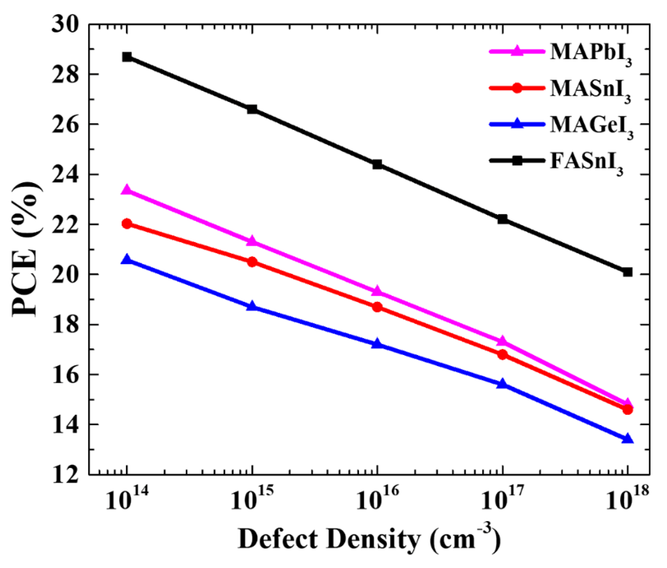
4.4. Influence of the Defect Density on the PCE

The overall PSC outputs of the current simulation are determined by another crucial parameter, i.e., defect densities. The performance of PSC is substantially impacted by the total defect density. Further, the trap energy levels serve as recombination centers and shorten carrier lifetimes. By applying chemical, material engineering, or compositional techniques, these defect levels can be passivated to lower the defect density and lengthen carrier lifetimes for improved performance.
These are why we consider the defect density (DD) analysis in the present study, as this method helps improve the PCE of PSCs. The defect density of the designed PSCs studied from 1 × 1014 cm−3 to 1 × 1018 cm−3, as shown in Figure 5. For all the PSC devices, the PCE value decreases with increasing defect density of the perovskite absorber materials. Specifically, the MAPbI3-based PSC reaches the PCE from 23.2% to 15.2%, whereas for MASnI3-based PSC, PCE drops from 22.01% to 15.4%, while for MAGeI3-based PSC, PCE drops from 20.3% to 13.2%, and finally for FASnI3 based PSC, the PCE decreases from 28.8% to 20.1%, when the defect density is reduced from 1 × 1014 cm−3 to 1 × 1018 cm−3, as presented in Figure 5.

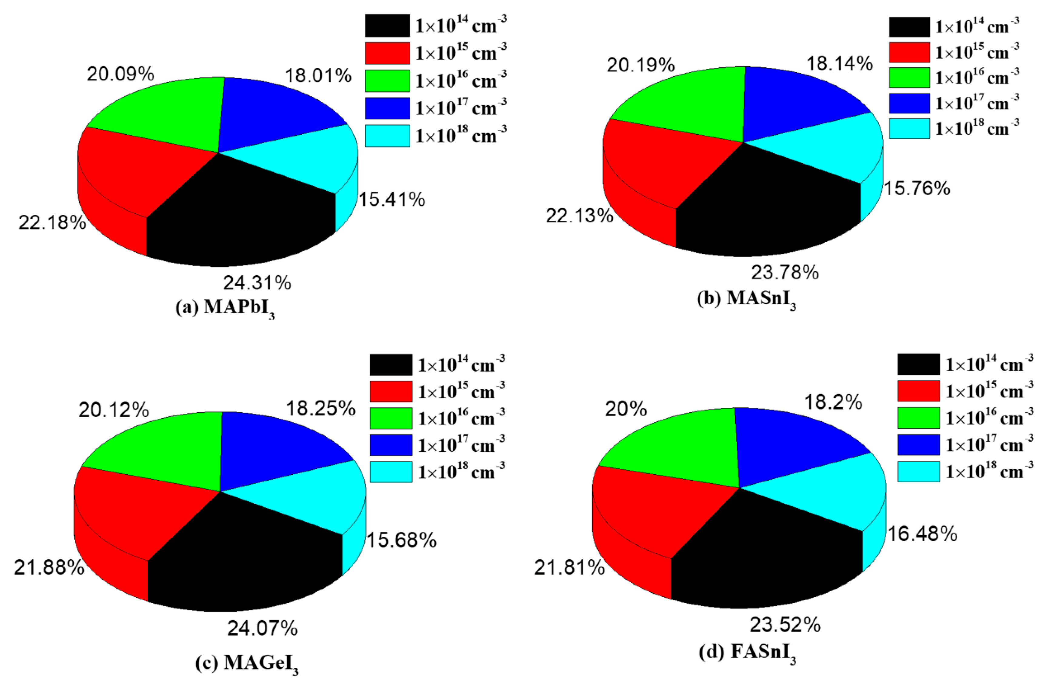
4.5. Pi-Diagram Analysis on the Efficiency of PSC

The pi chart (Figure 6) shows how many efficiency fractions are attained across the board for all simulated PSC devices. In particular, the pi chart may be used to determine how fractions vary in relation to defect densities. When building the gadget experimentally, imperfect dangling bonds arise during the material synthesis. These dangling bonds serve as the recombination center, increase the bandgap’s defect levels, and have an impact on the carrier lifespan and diffusion length. So, to carry out a realistic device simulation, we took into consideration bulk defect density inside the material to account for the defect-related recombination/carrier lifetime/diffusion duration. The Pi chart for the FASnI3-based PSC shows that the contribution of the FASnI3 absorber is only 23.52%, whereas the maximum fraction can be obtained for the MAPbI3-based PSC device, i.e., nearly 24.31% of the total defect density levels, as depicted in Figure 6.

4.6. EQE and J-V Parameters of PSC

The EQE is an essential optical measure in solar cell analysis. It provides a clear idea about the generation of photo carriers in that particular device. Having a band gap of 1.3 eV, MASnI3 responds up to 953 nm of wavelength. And maximum EQE of 90% is observed for MASnI3-based PSC in the wavelength ranges between 300 nm to 953 nm. Whereas MAGeI3 shows a reduced EQE as compared to the previous materials. The generation of photo carriers purely depends on the material quality and excitation coefficient of that material. As MASnI3 has a lower bandgap as compared to MAGeI3, it shows better EQE, as depicted in Figure 7. The result can be understood from the inverse dependability on the bandgap of the absorber material. As shown in Figure 7, the bandgap of MAPbI3 is 1.55 eV, so the EQE is up to the range of 800 nm, and for FASnI3, the bandgap is 1.41 eV, so the EQE is up to the wavelength value of 879 nm, respectively. The represented result is higher than the earlier reported value by Bhattarai et al. [71].
The current density (J) across the voltage (V) in the range of up to 1.8 V for the simulated PSC devices under lighting circumstances is shown in Figure 7b. It may be understood that the PSC shows the JSC that remains the same with increasing Voltage to 0.7 V for MAPbI3, 1.1 V for MASnI3 and FASnI3, and 1.3 V for MAGeI3, respectively. Also, the highest and the lowest VOC (1.79 V) and JSC (34.59 mA/cm2) are reached for MAGeI3 and MASnI3, respectively. But, the point to note is that the combination of JSC and VOC is maximum for the MA-free perovskite, i.e., FASnI3. The highest combination of JSC and VOC for FASnI3-based PSC is 34.59 mA/cm2 and 1.79 V, respectively. Moreover, due to the steeper curve in JV, the FF for the FASnI3-based PSC is maximum, i.e., nearly 88%. Due to the combination of all three parameters of the PSC, the maximum value of PCE may be attained for the FASnI3-based PSC. The work by Rai et al. shows the TiO2 and Cu2O as the ETL and HTL while the perovskite material is MAPb(I1-xClx)3. The work is being done with SCAPS-1D software (version 3.8). The detailed investigation of optoelectrical properties is accomplished to obtain the highest efficiency of the PSC. The optimization in thickness, bulk defect density, and interface defect density exclusively improve the JSC-VOC value. The current study offers much improved JSC-VOC than the prior value by Rai et al. [72], which obtained comparably a lower efficiency of 18.97%. Table 3 provides a thorough comparison with other relevant reports of the PSCs. The current work is the optimization of thickness, temperature, and defect density. Moreover, the analysis of defect density using the pi chart and EQE, J-V parameters are also accomplished. Optimization is important for obtaining the highest PCE of PSC devices. The proposed model offers the better-performing FASnI3-based PSC among all the proposed PSC devices. The comparison with earlier work and the PV parameters of JSC and VOC, and FF and PCE are listed in Table 3.

5. Conclusions

In conclusion, the detailed analysis and performance test for the different PSC devices have been accomplished with the help of the computational approach. We analyze the most crucial solar cell output characteristics using carrier transport mechanisms. The PAL of MAPbI3, MASnI3, MAGeI3, and FASnI3 are designed and studied to attain the best PSC device. Initially, the band energy diagram was studied to check the proper functioning of the PSC devices. The best absorber thickness for gaining maximum efficiency is one of the primary goals of the research work. Following that, the optimization of PAL at thickness shows that the maximum PCE of 28.69% was achieved for 600 nm for FASnI3-based PSC devices. Moreover, the defect density analysis shows an excellent efficiency of the FASnI3-based PSC at the defect density value of 1.0 × 1014 cm−3. Temperature analysis and Pi chart analysis were also conducted for the four PSC devices. As a result, the FASnI3-based PSC has a high JSC of 30.13 mA/cm2, VOC of 1.127 Volt, a high FF of nearly about 86.146%, and a PCE approaching 28.69%. Furthermore, the designed and investigated data for the FASnI3-based PSC offers an improved PCE than MA-based PSC devices. The exclusive study confirms a valuable guideline that has been shown to manufacture highly stable and suitable FASnI3-based PSC devices.

Author Contributions

Conceptualization, S.B. and M.K.H.; methodology, S.B.; software, S.B.; validation, S.B., M.K.A.M., J.M., R.P., H.A., L.B.F. and M.K.H.; formal analysis, S.B., M.K.A.M. and M.K.H.; investigation, S.B., J.M., R.P. and H.A.; resources, S.B. and M.K.H.; data curation, S.B., M.K.A.M. and M.K.H.; writing—original draft preparation, S.B.; writing—review and editing, S.B., M.K.A.M., J.M., R.P., H.A., L.B.F., M.A. and M.K.H.; visualization, S.B., M.K.A.M., J.M., R.P., H.A., L.B.F., M.A. and M.K.H.; funding acquisition, M.A. and M.K.H.; supervision, S.B. and M.K.H. project administration, S.B., L.B.F., M.A. and M.K.H. All authors have read and agreed to the published version of the manuscript.

Funding

This research is funded by King Khalid University, Saudi Arabia, under grant number R.G.P.2: 219/44.

Institutional Review Board Statement

Not applicable.

Informed Consent Statement

Not applicable.

Data Availability Statement

Not applicable.

Acknowledgments

The authors have extended their appreciation to the Deanship of Scientific Research at King Khalid University, Saudi Arabia, for funding this work through the Research Groups Program under grant number R.G.P.2: 219/44.

Conflicts of Interest

The authors declare no conflict of interest.

References

  1. Snaith, H.J. Perovskites: The Emergence of a New Era for Low-Cost, High-Efficiency Solar Cells. J. Phys. Chem. Lett. 2013, 4, 3623–3630. [Google Scholar] [CrossRef]
  2. Ebner, M.; Marone, F.; Stampanoni, M.; Wood, V. Visualization and Quantification of Electrochemical and Mechanical Degradation in Li Ion Batteries. Science 2013, 342, 716–720. [Google Scholar] [CrossRef] [PubMed]
  3. Conings, B.; Drijkoningen, J.; Gauquelin, N.; Babayigit, A.; D’Haen, J.; D’Olieslaeger, L.; Ethirajan, A.; Verbeeck, J.; Manca, J.; Mosconi, E.; et al. Intrinsic Thermal Instability of Methylammonium Lead Trihalide Perovskite. Adv. Energy Mater. 2015, 5, 1500477. [Google Scholar] [CrossRef]
  4. Isikgor, F.H.; Zhumagali, S.; Merino, L.V.T.; De Bastiani, M.; McCulloch, I.; De Wolf, S. Molecular Engineering of Contact Interfaces for High-Performance Perovskite Solar Cells. Nat. Rev. Mater. 2022, 8, 89–108. [Google Scholar] [CrossRef]
  5. Bati, A.S.R.; Zhong, Y.L.; Burn, P.L.; Nazeeruddin, M.K.; Shaw, P.E.; Batmunkh, M. Next-Generation Applications for Integrated Perovskite Solar Cells. Commun. Mater. 2023, 4, 2. [Google Scholar] [CrossRef]
  6. Min, J.; Demchyshyn, S.; Sempionatto, J.R.; Song, Y.; Hailegnaw, B.; Xu, C.; Yang, Y.; Solomon, S.; Putz, C.; Lehner, L.E.; et al. An Autonomous Wearable Biosensor Powered by a Perovskite Solar Cell. Nat. Electron. 2023. [Google Scholar] [CrossRef]
  7. Li, G.; Su, Z.; Canil, L.; Hughes, D.; Aldamasy, M.H.; Dagar, J.; Trofimov, S.; Wang, L.; Zuo, W.; Jerónimo-Rendon, J.J.; et al. Highly Efficient P-i-n Perovskite Solar Cells That Endure Temperature Variations. Science 2023, 379, 399–403. [Google Scholar] [CrossRef]
  8. Yang, M.; Tian, T.; Fang, Y.; Li, W.-G.; Liu, G.; Feng, W.; Xu, M.; Wu, W.-Q. Reducing Lead Toxicity of Perovskite Solar Cells with a Built-in Supramolecular Complex. Nat. Sustain. 2023. [Google Scholar] [CrossRef]
  9. Xiao, H.; Zuo, C.; Yan, K.; Jin, Z.; Cheng, Y.; Tian, H.; Xiao, Z.; Liu, F.; Ding, Y.; Ding, L. Highly Efficient and Air-Stable Inorganic Perovskite Solar Cells Enabled by Polylactic Acid Modification. Adv. Energy Mater. 2023. [Google Scholar] [CrossRef]
  10. Park, S.M.; Wei, M.; Xu, J.; Atapattu, H.R.; Eickemeyer, F.T.; Darabi, K.; Grater, L.; Yang, Y.; Liu, C.; Teale, S.; et al. Engineering Ligand Reactivity Enables High-Temperature Operation of Stable Perovskite Solar Cells. Science 2023, 381, 209–215. [Google Scholar] [CrossRef]
  11. Mohammed, M.K.A.; Al-Mousoi, A.K.; Kumar, A.; Katae, A.R.J.; Khaleel, O.A.; Ahmed, D.S.; Hossain, M.K. Fluorinated Carbon Nanotubes: A Low-Cost Hole Transport Layer for Perovskite Solar Cells. J. Mater. Sci. 2023, 58, 11748–11760. [Google Scholar] [CrossRef]
  12. Peng, W.; Mao, K.; Cai, F.; Meng, H.; Zhu, Z.; Li, T.; Yuan, S.; Xu, Z.; Feng, X.; Xu, J.; et al. Reducing Nonradiative Recombination in Perovskite Solar Cells with a Porous Insulator Contact. Science 2023, 379, 683–690. [Google Scholar] [CrossRef] [PubMed]
  13. McMeekin, D.P.; Holzhey, P.; Fürer, S.O.; Harvey, S.P.; Schelhas, L.T.; Ball, J.M.; Mahesh, S.; Seo, S.; Hawkins, N.; Lu, J.; et al. Intermediate-Phase Engineering via Dimethylammonium Cation Additive for Stable Perovskite Solar Cells. Nat. Mater. 2023, 22, 73–83. [Google Scholar] [CrossRef]
  14. Liu, M.; Johnston, M.B.; Snaith, H.J. Efficient Planar Heterojunction Perovskite Solar Cells by Vapour Deposition. Nature 2013, 501, 395–398. [Google Scholar] [CrossRef]
  15. Riaz, M.; Earles, S.K.; Kadhim, A.; Azzahrani, A. Computer Analysis of Microcrystalline Silicon Hetero-Junction Solar Cell with Lumerical FDTD/DEVICE. Int. J. Comput. Mater. Sci. Eng. 2017, 06, 1750017. [Google Scholar] [CrossRef]
  16. Ahmed, M.I.; Habib, A.; Javaid, S.S. Perovskite Solar Cells: Potentials, Challenges, and Opportunities. Int. J. Photoenergy 2015, 2015, 1–13. [Google Scholar] [CrossRef]
  17. (Balu) Balachandran, U.; Lee, T.H.; Park, C.Y.; Emerson, J.E.; Picciolo, J.J.; Dorris, S.E. Dense Cermet Membranes for Hydrogen Separation. Sep. Purif. Technol. 2014, 121, 54–59. [Google Scholar] [CrossRef]
  18. Tchognia, J.H.N.; Arba, Y.; Dakhsi, K.; Hartiti, B.; Ridah, A.; Tchognia, J.H.N.; Ndjaka, J.-M.; Thevenin, P. Optimization of the Output Parameters in Kesterite-Based Solar Cells by AMPS-1D. In Proceedings of the 2015 3rd International Renewable and Sustainable Energy Conference (IRSEC), Marrakech, Morocco, 10–13 December 2015; pp. 1–6. [Google Scholar]
  19. Kojima, A.; Teshima, K.; Shirai, Y.; Miyasaka, T. Organometal Halide Perovskites as Visible-Light Sensitizers for Photovoltaic Cells. J. Am. Chem. Soc. 2009, 131, 6050–6051. [Google Scholar] [CrossRef]
  20. Kwon, H.-C.; Ma, S.; Yun, S.-C.; Jang, G.; Yang, H.; Moon, J. A Nanopillar-Structured Perovskite-Based Efficient Semitransparent Solar Module for Power-Generating Window Applications. J. Mater. Chem. A 2020, 8, 1457–1468. [Google Scholar] [CrossRef]
  21. Noh, J.H.; Im, S.H.; Heo, J.H.; Mandal, T.N.; Seok, S. Il Chemical Management for Colorful, Efficient, and Stable Inorganic–Organic Hybrid Nanostructured Solar Cells. Nano Lett. 2013, 13, 1764–1769. [Google Scholar] [CrossRef]
  22. Tan, H.Q.; Zhao, X.; Birgersson, E.; Lin, F.; Xue, H. Optoelectronic Modeling and Sensitivity Analysis of a Four-Terminal All-Perovskite Tandem Solar Cell – Identifying Pathways to Improve Efficiency. Sol. Energy 2021, 216, 589–600. [Google Scholar] [CrossRef]
  23. Jiang, Y.; Juarez-Perez, E.J.; Ge, Q.; Wang, S.; Leyden, M.R.; Ono, L.K.; Raga, S.R.; Hu, J.; Qi, Y. Post-Annealing of MAPbI3 Perovskite Films with Methylamine for Efficient Perovskite Solar Cells. Mater. Horiz. 2016, 3, 548–555. [Google Scholar] [CrossRef]
  24. Chen, L.-C.; Weng, C.-Y. Optoelectronic Properties of MAPbI3 Perovskite/Titanium Dioxide Heterostructures on Porous Silicon Substrates for Cyan Sensor Applications. Nanoscale Res. Lett. 2015, 10, 404. [Google Scholar] [CrossRef] [PubMed]
  25. Azri, F.; Meftah, A.; Sengouga, N.; Meftah, A. Electron and Hole Transport Layers Optimization by Numerical Simulation of a Perovskite Solar Cell. Sol. Energy 2019, 181, 372–378. [Google Scholar] [CrossRef]
  26. Raoui, Y.; Ez-Zahraouy, H.; Tahiri, N.; El Bounagui, O.; Ahmad, S.; Kazim, S. Performance Analysis of MAPbI3 Based Perovskite Solar Cells Employing Diverse Charge Selective Contacts: Simulation Study. Sol. Energy 2019, 193, 948–955. [Google Scholar] [CrossRef]
  27. Bhattarai, S.; Das, T.D. Optimization of Carrier Transport Materials for the Performance Enhancement of the MAGeI3 Based Perovskite Solar Cell. Sol. Energy 2021, 217, 200–207. [Google Scholar] [CrossRef]
  28. Zhao, F.; Feng, Y.; Feng, W. Germanium-based Monoelemental and Binary Two-dimensional Materials: Theoretical and Experimental Investigations and Promising Applications. InfoMat 2022, 4, e12365. [Google Scholar] [CrossRef]
  29. Guo, H.; Hou, F.; Ren, X.; Ning, X.; Wang, Y.; Yang, H.; Wei, J.; Guo, J.; Li, T.; Zhu, C.; et al. Recent Progresses on Transparent Electrodes and Active Layers Toward Neutral, Color Semitransparent Perovskite Solar Cells. Sol. RRL 2023. [Google Scholar] [CrossRef]
  30. Meng, X.; Lin, J.; Liu, X.; He, X.; Wang, Y.; Noda, T.; Wu, T.; Yang, X.; Han, L. Highly Stable and Efficient FASnI3-Based Perovskite Solar Cells by Introducing Hydrogen Bonding. Adv. Mater. 2019, 31, 1903721. [Google Scholar] [CrossRef]
  31. Kayesh, M.E.; Chowdhury, T.H.; Matsuishi, K.; Kaneko, R.; Kazaoui, S.; Lee, J.-J.; Noda, T.; Islam, A. Enhanced Photovoltaic Performance of FASnI3-Based Perovskite Solar Cells with Hydrazinium Chloride Coadditive. ACS Energy Lett. 2018, 3, 1584–1589. [Google Scholar] [CrossRef]
  32. Gu, W.; Xu, X.; Chen, J.; Ma, B.; Qin, M.; Zhu, W.; Qian, J.; Qin, Z.; Shen, W.; Lu, Y.; et al. Oriented Perovskite Crystal towards Efficient Charge Transport in FASnI3 Perovskite Solar Cells. Sol. RRL 2020, 4, 2000153. [Google Scholar] [CrossRef]
  33. Meng, X.; Wang, Y.; Lin, J.; Liu, X.; He, X.; Barbaud, J.; Wu, T.; Noda, T.; Yang, X.; Han, L. Surface-Controlled Oriented Growth of FASnI3 Crystals for Efficient Lead-Free Perovskite Solar Cells. Joule 2020, 4, 902–912. [Google Scholar] [CrossRef]
  34. Zillner, J.; Boyen, H.; Schulz, P.; Hanisch, J.; Gauquelin, N.; Verbeeck, J.; Küffner, J.; Desta, D.; Eisele, L.; Ahlswede, E.; et al. The Role of SnF2 Additive on Interface Formation in All Lead-Free FASnI3 Perovskite Solar Cells. Adv. Funct. Mater. 2022, 32, 2109649. [Google Scholar] [CrossRef]
  35. Liu, X.; Wu, T.; Chen, J.-Y.; Meng, X.; He, X.; Noda, T.; Chen, H.; Yang, X.; Segawa, H.; Wang, Y.; et al. Templated Growth of FASnI3 Crystals for Efficient Tin Perovskite Solar Cells. Energy Environ. Sci. 2020, 13, 2896–2902. [Google Scholar] [CrossRef]
  36. Chiang, C.-H.; Lin, J.-W.; Wu, C.-G. One-Step Fabrication of a Mixed-Halide Perovskite Film for a High-Efficiency Inverted Solar Cell and Module. J. Mater. Chem. A 2016, 4, 13525–13533. [Google Scholar] [CrossRef]
  37. Dong, Z.; Li, W.; Wang, H.; Jiang, X.; Liu, H.; Zhu, L.; Chen, H. High-Temperature Perovskite Solar Cells. Sol. RRL 2021, 5, 2100370. [Google Scholar] [CrossRef]
  38. Devi, C.; Mehra, R. Device Simulation of Lead-Free MASnI3 Solar Cell with CuSbS2 (Copper Antimony Sulfide). J. Mater. Sci. 2019, 54, 5615–5624. [Google Scholar] [CrossRef]
  39. Thakur, A.; Singh, D.; Kaur Gill, S. Numerical Simulations of 26.11% Efficient Planar CH3NH3PbI3 Perovskite n-i-p Solar Cell. Mater. Today Proc. 2022, 71, 195–201. [Google Scholar] [CrossRef]
  40. Pandey, R.; Khanna, A.; Singh, K.; Patel, S.K.; Singh, H.; Madan, J. Device Simulations: Toward the Design of >13% Efficient PbS Colloidal Quantum Dot Solar Cell. Sol. Energy 2020, 207, 893–902. [Google Scholar] [CrossRef]
  41. Dureja, T.; Garg, A.; Bhalla, S.; Bhutani, D.; Khanna, A. Double Lead-Free Perovskite Solar Cell for 19.9% Conversion Efficiency: A SCAPS-1D Based Simulation Study. Mater. Today Proc. 2022, 71, 239–242. [Google Scholar] [CrossRef]
  42. Divitini, G.; Cacovich, S.; Matteocci, F.; Cinà, L.; Di Carlo, A.; Ducati, C. In Situ Observation of Heat-Induced Degradation of Perovskite Solar Cells. Nat. Energy 2016, 1, 15012. [Google Scholar] [CrossRef]
  43. Li, X.; Yang, J.; Jiang, Q.; Lai, H.; Li, S.; Xin, J.; Chu, W.; Hou, J. Low-Temperature Solution-Processed ZnSe Electron Transport Layer for Efficient Planar Perovskite Solar Cells with Negligible Hysteresis and Improved Photostability. ACS Nano 2018, 12, 5605–5614. [Google Scholar] [CrossRef]
  44. Mathur, A.S.; Dubey, S.; Nidhi; Singh, B.P. Study of Role of Different Defects on the Performance of CZTSe Solar Cells Using SCAPS. Optik 2020, 206, 163245. [Google Scholar] [CrossRef]
  45. Tan, H.; Che, F.; Wei, M.; Zhao, Y.; Saidaminov, M.I.; Todorović, P.; Broberg, D.; Walters, G.; Tan, F.; Zhuang, T.; et al. Dipolar Cations Confer Defect Tolerance in Wide-Bandgap Metal Halide Perovskites. Nat. Commun. 2018, 9, 3100. [Google Scholar] [CrossRef]
  46. Alipour, H.; Ghadimi, A. Optimization of Lead-Free Perovskite Solar Cells in Normal-Structure with WO3 and Water-Free PEDOT: PSS Composite for Hole Transport Layer by SCAPS-1D Simulation. Opt. Mater. 2021, 120, 111432. [Google Scholar] [CrossRef]
  47. Hossain, M.K.; Toki, G.F.I.; Kuddus, A.; Mohammed, M.K.A.; Pandey, R.; Madan, J.; Bhattarai, S.; Rahman, M.F.; Dwivedi, D.K.; Amami, M.; et al. Optimization of the Architecture of Lead-Free CsSnCl3-Perovskite Solar Cells for Enhancement of Efficiency: A Combination of SCAPS-1D and WxAMPS Study. Mater. Chem. Phys. 2023, 308, 128281. [Google Scholar] [CrossRef]
  48. Roy, P.; Kumar Sinha, N.; Tiwari, S.; Khare, A. A Review on Perovskite Solar Cells: Evolution of Architecture, Fabrication Techniques, Commercialization Issues and Status. Sol. Energy 2020, 198, 665–688. [Google Scholar] [CrossRef]
  49. Rahman, M.S.; Miah, S.; Marma, M.S.W.; Ibrahim, M. Numerical Simulation of CsSnI3-Based Perovskite Solar Cells: Influence of Doped-ITO Front Contact. In Proceedings of the 2020 IEEE REGION 10 CONFERENCE (TENCON), Osaka, Japan, 16–19 November 2020; pp. 140–145. [Google Scholar] [CrossRef]
  50. Khatoon, S.; Chakraborty, V.; Yadav, S.K.; Diwakar, S.; Singh, J.; Singh, R.B. Simulation Study of CsPbIxBr1-x and MAPbI3 Heterojunction Solar Cell Using SCAPS-1D. Sol. Energy 2023, 254, 137–157. [Google Scholar] [CrossRef]
  51. Zhang, X.; Zhou, H.; Hu, C.; Zhao, Y.; Ma, X.; Wu, J.; Qi, Y.; Fang, W.; Jia, S.; Yu, J. Performance Analysis of All-Inorganic Cs3Sb2I9 Perovskite Solar Cells with Micro-Offset Energy Level Structure by SCAPS-1D Simulation and First-Principles Calculation. Sol. Energy Mater. Sol. Cells 2023, 260, 112487. [Google Scholar] [CrossRef]
  52. Mushtaq, S.; Tahir, S.; Ashfaq, A.; Sebastian Bonilla, R.; Haneef, M.; Saeed, R.; Ahmad, W.; Amin, N. Performance Optimization of Lead-Free MASnBr3 Based Perovskite Solar Cells by SCAPS-1D Device Simulation. Sol. Energy 2023, 249, 401–413. [Google Scholar] [CrossRef]
  53. Hossain, M.K.; Toki, G.F.I.; Kuddus, A.; Rubel, M.H.K.; Hossain, M.M.; Bencherif, H.; Rahman, M.F.; Islam, M.R.; Mushtaq, M. An Extensive Study on Multiple ETL and HTL Layers to Design and Simulation of High-Performance Lead-Free CsSnCl3-Based Perovskite Solar Cells. Sci. Rep. 2023, 13, 2521. [Google Scholar] [CrossRef] [PubMed]
  54. Ravidas, B.K.; Roy, M.K.; Samajdar, D.P. Investigation of Photovoltaic Performance of Lead-Free CsSnI3-Based Perovskite Solar Cell with Different Hole Transport Layers: First Principle Calculations and SCAPS-1D Analysis. Sol. Energy 2023, 249, 163–173. [Google Scholar] [CrossRef]
  55. Park, N.-G. Methodologies for High Efficiency Perovskite Solar Cells. Nano Converg. 2016, 3, 15. [Google Scholar] [CrossRef] [PubMed]
  56. Metin, B.; Kavasoglu, N.; Kavasoglu, A.S. AFORS-HET Simulation for Investigating the Performance of ZnO/n-CdS/p-CdTe /Ag Solar Cell Depending on CdTe Acceptor Concentration and Temperature. Phys. B Condens. Matter 2023, 649, 414504. [Google Scholar] [CrossRef]
  57. Kumar, M.; Kumar, S. 24.13% Efficient TiO2/i–a–Si:H/p–c–Si Heterojunction Solar Cell by AFORS-HET Numerical Simulation. Opt. Quantum Electron. 2023, 55, 441. [Google Scholar] [CrossRef]
  58. Singh, A.; Ghosh, R.; Agarwal, P. Selection of Materials and Optimization of Antireflection Coatings for Silicon Solar Cells Using Sentaurus TCAD. J. Mater. Sci. Mater. Electron. 2023, 34, 1235. [Google Scholar] [CrossRef]
  59. Okil, M.; Shaker, A.; Ahmed, I.S.; Abdolkader, T.M.; Salem, M.S. Evaluation of a Proposed Barium Di-Silicide Tandem Solar Cell Using TCAD Numerical Simulation. Opt. Quantum Electron. 2023, 55, 475. [Google Scholar] [CrossRef]
  60. Boukortt, N.E.I.; Patanè, S.; AlAmri, A.M.; AlAjmi, D.; Bulayyan, K.; AlMutairi, N. Numerical Investigation of Perovskite and U-CIGS Based Tandem Solar Cells Using Silvaco TCAD Simulation. Silicon 2023, 15, 293–303. [Google Scholar] [CrossRef]
  61. Seboui, Z.; Dabbabi, S. First Investigation on CZTS Electron Affinity and Thickness Optimization Using SILVACO-Atlas 2D Simulation. Simul. Model. Pract. Theory 2023, 126, 102758. [Google Scholar] [CrossRef]
  62. Mahmoud, A.H.K.; Hameed, M.F.O.; Hussein, M.; Obayya, S.S.A. Optical and Electrical Characteristics of Highly Efficient Flower-Shaped Silicon Nanowires Solar Cell. Opt. Quantum Electron. 2023, 55, 341. [Google Scholar] [CrossRef]
  63. Agnihotri, S.K.; Prashant, D.V.; Samajdar, D.P. Theoretical Insights into the Coupled Optoelectronic Analysis of InP Truncated Nanopyramid/Germanium Ttandem Solar Cells. Sol. Energy 2023, 249, 327–335. [Google Scholar] [CrossRef]
  64. Teimouri, R.; Heydari, Z.; Ghaziani, M.P.; Madani, M.; Abdy, H.; Kolahdouz, M.; Asl-Soleimani, E. Synthesizing Li Doped TiO2 Electron Transport Layers for Highly Efficient Planar Perovskite Solar Cell. Superlattices Microstruct. 2020, 145, 106627. [Google Scholar] [CrossRef]
  65. Liu, G.; Zhong, Y.; Mao, H.; Yang, J.; Dai, R.; Hu, X.; Xing, Z.; Sheng, W.; Tan, L.; Chen, Y. Highly Efficient and Stable ZnO-Based MA-Free Perovskite Solar Cells via Overcoming Interfacial Mismatch and Deprotonation Reaction. Chem. Eng. J. 2022, 431, 134235. [Google Scholar] [CrossRef]
  66. Abena, A.M.N.; Ngoupo, A.T.; Abega, F.X.A.; Ndjaka, J.M.B. Numerical Investigation of Solar Cells Based on Hybrid Organic Cation Perovskite with Inorganic HTL via SCAPS-1D. Chin. J. Phys. 2022, 76, 94–109. [Google Scholar] [CrossRef]
  67. Pindolia, G.; Shinde, S.M.; Jha, P.K. Optimization of an Inorganic Lead Free RbGeI3 Based Perovskite Solar Cell by SCAPS-1D Simulation. Sol. Energy 2022, 236, 802–821. [Google Scholar] [CrossRef]
  68. Bhattarai, S.; Hossain, I.; Maiti, M.; Pandey, R.; Madan, J. Performance Analysis and Optimization of All-Inorganic CsPbI3-Based Perovskite Solar Cell. Indian J. Phys. 2023, 97, 2629–2637. [Google Scholar] [CrossRef]
  69. Bhattarai, S.; Pandey, R.; Madan, J.; Mhamdi, A.; Bouazizi, A.; Muchahary, D.; Gogoi, D.; Sharma, A.; Das, T.D. Investigation of Carrier Transport Materials for Performance Assessment of Lead-Free Perovskite Solar Cells. IEEE Trans. Electron Devices 2022, 69, 3217–3224. [Google Scholar] [CrossRef]
  70. Tara, A.; Bharti, V.; Sharma, S.; Gupta, R. Device Simulation of FASnI3 Based Perovskite Solar Cell with Zn(O0.3, S0.7) as Electron Transport Layer Using SCAPS-1D. Opt. Mater. 2021, 119, 111362. [Google Scholar] [CrossRef]
  71. Bhattarai, S.; Sharma, A.; Das, T.D. Efficiency Enhancement of Perovskite Solar Cell by Using Doubly Carrier Transport Layers with a Distinct Bandgap of MAPbI3 Active Layer. Optik 2020, 224, 165430. [Google Scholar] [CrossRef]
  72. Rai, S.; Pandey, B.K.; Dwivedi, D.K. Modeling of Highly Efficient and Low Cost CH3NH3Pb(I1-xClx)3 Based Perovskite Solar Cell by Numerical Simulation. Opt. Mater. 2020, 100, 109631. [Google Scholar] [CrossRef]
  73. Abdelaziz, S.; Zekry, A.; Shaker, A.; Abouelatta, M. Investigating the Performance of Formamidinium Tin-Based Perovskite Solar Cell by SCAPS Device Simulation. Opt. Mater. 2020, 101, 109738. [Google Scholar] [CrossRef]
Figure 1. (a) Digramic illustration of layer structures with Spiro-OMeTAD/ZnO as the CTLs (HTL/ETL) and (b) working principle using energy level diagram with reference to the vacuum energy level in the solar designs.
Sustainability 15 12805 g001
Figure 2. (ad) Energy band diagram (EBD) representation of four different PSC devices.
Sustainability 15 12805 g002
Figure 3. (ad) Variations in VOC, JSC, FF, and PCE concerning increasing PAL thickness.
Sustainability 15 12805 g003
Figure 4. Variations in conversion efficiency (PCE) with respect to temperature.
Sustainability 15 12805 g004
Figure 5. Variations in conversion efficiency (PCE) with respect to defect density of the PAL.
Sustainability 15 12805 g005
Figure 6. Pi-chart variation for studying the PCE with respect to individual defect density.
Sustainability 15 12805 g006
Figure 7. Variations in (a) EQE and (b) J over V diagram for all four PSC devices.
Sustainability 15 12805 g007
Table 1. Simulating parameters in SCAPS-1D for the different absorber materials.
Parameters SymbolZnOMAPbI3MASnI3MAGeI3FASnI3Spiro-OMeTAD
d100200–800100100100100
Eg (eV)3.31.551.31.91.413.0
χ (eV)4.13.94.13.983.522.45
ɛr96.58.2108.23
Nc (m−3)4 × 10182.2 × 10181 × 10181 × 10161 × 10181 × 1019
Nv (m−3)4 × 10191.8 × 10191 × 10181 × 10151 × 10181 × 1019
ve (cm/s)1 × 1071 × 1071 × 1071 × 1071 × 1071 × 107
vh (cm/s)1 × 1071 × 1071 × 1071 × 1071 × 1071 × 107
µn (cm2/Vs)10021.61.62 × 101222 × 10−4
µp (cm2/Vs)2521.61.01 × 101222 × 10−4
Nd (cm−3)1 × 10185.21 × 10901 × 10900
Na (cm−3)1 × 1055.21 × 1091 × 10151 × 1097 × 10162 × 1018
Nt (cm−3)1 × 10151 × 10141 × 10141 × 10141 × 10141 × 1015
References[69][25][69][27][70][27]
Table 2. Parameter of interface (IF) defects utilized in SCAPS simulations.
ParametersSpiro-OMeTAD/PALPAL/ZnO
Defect typesNeutralNeutral
Cap. cross-section electrons (cm2)1 × 10−191 × 10−19
Cap. cross-section holes (cm2)1 × 10−191 × 10−19
Energy distributionssinglesingle
Reference for defect energy levelAbove the highest EVAbove the highest EV
Energy wrt reference (eV)0.60.6
Total density (integrated over all energies) (cm−2)1 × 10101 × 1010
Table 3. The PV performances of different PSC devices.
PSC Device StructuresVOC (V)Jsc (mA cm−2)FF (%)PCE (%)
ITO/ZnO/MAPbI3/Spiro-OMeTAD/Au1.16123.884.4823.35
ITO/ZnO/MASnI3/Spiro-OMeTAD/Au0.87433.5574.6221.88
ITO/ZnO/MAGeI3/Spiro-OMeTAD/Au1.4719.2266.7618.95
ITO/ZnO/FASnI3/Spiro-OMeTAD/Au1.12730.1386.14628.69
ITO/ZnO/MAPbI3/CuSCN/Ag [25]1.2721.8983.7023.30
FTO/PCBM/MAPbI3/PEDOT: PSS + WO3/Cu [38]0.8623.2374.9414.96
FTO/Zn(O0.3, S0.7)/FASnI3/CuSCN/Au [70]1.08628.1284.9625.94
FTO/TiO2/FASnI3/Spiro-OMeTAD/Au [73]0.91522.6567.7414.03
Disclaimer/Publisher’s Note: The statements, opinions and data contained in all publications are solely those of the individual author(s) and contributor(s) and not of MDPI and/or the editor(s). MDPI and/or the editor(s) disclaim responsibility for any injury to people or property resulting from any ideas, methods, instructions or products referred to in the content.

