Article

Unified Modeling and Double-Loop Controller Design of Three-Level Boost Converter

1
LG Magna. co.kr, Incheon 22744, Republic of Korea
2
Faculty of Electrical Engineering, Korea National University of Transportation, Chungju si 27469, Republic of Korea
*
Author to whom correspondence should be addressed.
Sustainability 2023, 15(2), 1597; https://doi.org/10.3390/su15021597
Submission received: 5 November 2022 / Revised: 3 January 2023 / Accepted: 6 January 2023 / Published: 13 January 2023

Abstract

:
A new small-signal modeling of a three-level boost (TLB) converter, as well as the design methodology for a double-loop controller, are presented in this paper. Unlike the conventional modeling of the TLB converter, which involves three state variables, the suggested modeling is based on two state variables; hence, simple transfer functions can be obtained. The proposed method is operable at a full duty ratio using unified modeling approaches, regardless of the mode changes. The analysis shows that the transfer functions of the two operation modes are identical. This suggests that the small-signal modeling of the TLB converter is identical to that of a conventional single-level boost converter. Hence, this implies that a linear feedback controller is applicable for all operational ranges. The method to design a double-loop controller using a proportional-integral controller is shown in a stepwise sequence. In addition, a capacitor voltage unbalancing controller is described. Simulations and experimental verifications are conducted to verify the effectiveness of the small-signal analysis and control system design.

1. Introduction

Recently, the use of renewable energy sources such as photovoltaic (PV) and fuel cells have increased steadily, owing to environmental pollution and soaring oil prices. These renewable energy sources must be boosted up to high DC voltages of 350 to 400 [V] for linkage in a grid-connected system, owing to their relatively low DC voltage output of 20 to 50 [V]. A conventional single-level boost converter is typically used for this purpose. However, contrary to the theoretical five- to six-fold boost in voltage, the boost ratio is limited to two to three times, owing to the equivalent series resistance (ESR) component of the inductor. In addition, the voltage and current stress on the switch increase with the power level, thereby increasing the price of the switch or disenabling an appropriate switch to be obtained [1,2,3].
Many converter topologies for high-conversion-ratio and high-voltage applications have been studied to overcome the aforementioned problems [4,5,6,7,8,9]. Among them, the three-level boost (TLB) converter is a topology typically used, owing to its advantages compared with single-level boost converters [10,11], i.e., (i) the reduced inductor size because the equivalent switching frequency applied to the inductor current is doubled; and (ii) the reduced voltage and current stress because the voltage applied by each switch is half the output voltage. The TLB converter circuit is shown in the upper part of Figure 1.
However, the TLB converter topology has several disadvantages, such as the voltage imbalance and a complex control structure. The voltage imbalance occurs in the output capacitors, owing to their mismatched components, such as the duty ratio, capacitance, and ESR [12,13,14,15]. A TLB converter requires a complex controller because two different current paths are formed when the duty ratio is less than or larger than 0.5 [16,17,18]. The controller gains should be switched when the duty ratio crosses the boundary of 0.5. This renders it difficult to design a linear controller that is operable at a full duty ratio. Previous related studies are based on the third-order state-space equation, which complicates the system transfer functions.
Moreover, the TLB converter has a right-half-plane zero and hence a non-minimum phase system, resulting in unstable voltage regulation. Additionally, it can be a significant problem when the TLB converter is operated in the voltage regulation mode, owing to the uncontrolled inductor current, which can damage the switching device if the duty ratio increases. Therefore, a double-loop controller comprising a current controller in the inner loop and a voltage controller in the outer loop should be developed. Most previous studies do not address the problems of TLB converters.
The objective of this paper is to introduce a unified modeling method that is applicable to a full duty ratio. The proposed modeling method assumes a continuous conduction mode (CCM) of the inductor current. The unified state-space equation is derived by considering the output voltage instead of the capacitor voltage as a state variable. The suggested state-space equation becomes a second-order system that is operable at a full duty ratio, regardless of the boundary of 0.5. Therefore, the transfer functions are simple and easy to implement in a linear controller. The method for the voltage regulation system based on a double loop is presented in a stepwise sequence herein.
The proposed controller configuration of the TLB converter is shown in Figure 1. The controller is composed of a double-loop controller and a voltage-balancing controller. The double-loop controller controls the inductor current and the capacitor output voltage simultaneously, whereas the voltage-balancing controller controls the output capacitor voltages to the same voltage level. The sum or subtraction of these two controller outputs is used as the comparator inputs to generate the PWM signal of each switch.
The main section is composed as follows: First, the average state-space equation of each mode is analyzed, and a unified equation is obtained by combining each mode operation. Subsequently, the design of the double-loop controller is presented as a stepwise procedure in the next section. Finally, the simulation and experimental results are presented in the final section to demonstrate the validity of the proposed modeling methods and controller design.
The proposed modeling method is unique and original. The merit of the proposed method is simple and utilizes an easy to design controller using a unified modeling approach.

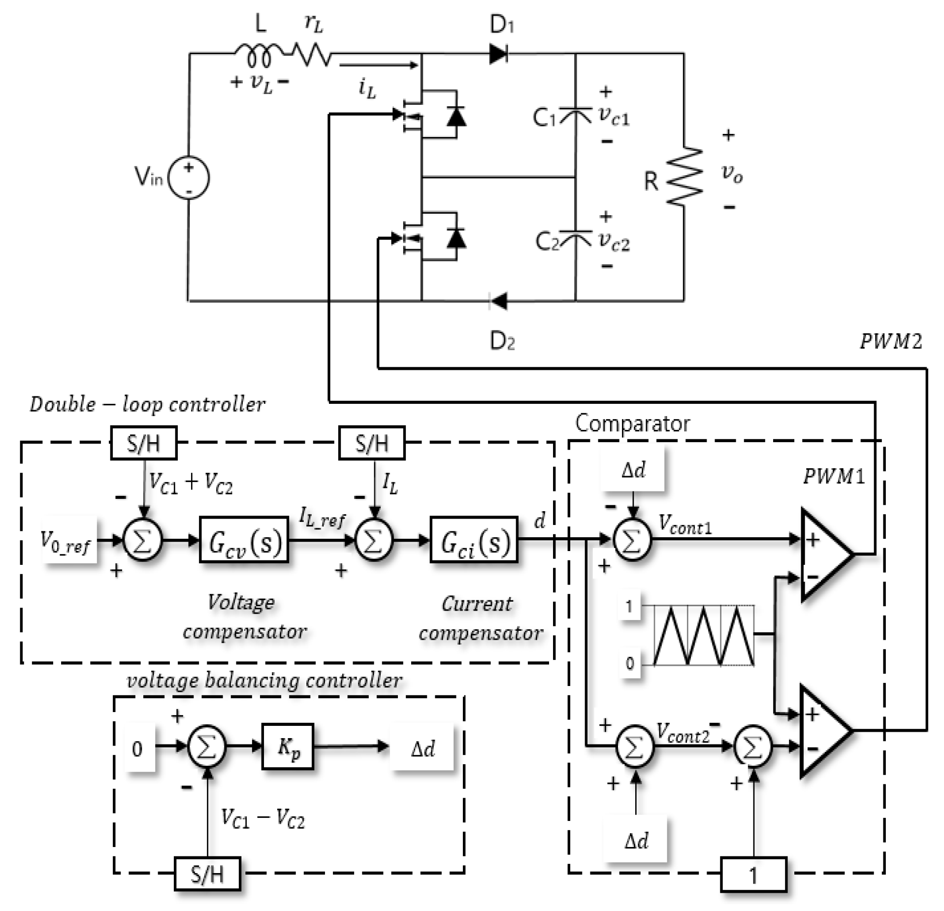
2. Proposed Unified Modeling of TLB Converter

In actual applications, each switch in the TLB converter is controlled by a combination of the control duty (d) determined by a double-loop controller, and the compensator duty ( Δ d ) determined by the voltage unbalancing controller, as shown in Figure 1. Switch S1 is controlled by the control signal, V cont 1 , which is expressed as (d − Δ d ), whereas S2 is controlled by the control signal, V cont 2 which is expressed as (d + Δ d ) [19,20,21,22]. The compensator signal Δ d can be considered as zero because its values are extremely small in the steady state. Therefore, the control signals of switches 1 and 2 in each mode can be considered to have the same value and are operated on a phase shift of 180°. The average state-space equation of the TLB converter model can be obtained as follows: Two modes (Modes 1 and 2) exist depending on the duty ratio boundary of 0.5. Because three operation states exist for each mode, the state-space equation of each mode can be obtained by averaging the three-state operation. The ideal operation waveforms of each mode of the TLB converter are shown in Figure 2. Mode 1 (Figure 2a) corresponds to a duty ratio of more than 0.5, whereas Mode 2 (Figure 2b) corresponds to a duty ratio of less than 0.5.
When deriving the state-space equation of the converter, the capacitor voltage and inductor current are generally defined as state variables, i.e., for N status variables, N-th order equations are obtained. Because two capacitors are connected to the output stage in the TLB converter, the state-space equations will be expressed as third-order equations. Complex mathematical calculations are required for small-signal analysis owing to the high-order system. Consequently, a linear controller that is operable at a full duty range becomes difficult to design.
Unlike the conventional method, the following were assumed in this study to analyze the converter operation using only two state variables. The capacitor voltage ( v c 1 , v c 2 ) can be expressed as a continuous linear voltage at each operation state.
Therefore, the output voltage ( v o ) can be expressed as the sum of each capacitor voltage in Equation (1):
v o ( t ) = v c 1 ( t ) + v c 2 ( t )
Differentiating the equation above, the Equation (2) can be derived:
dv o ( t ) dt = dv c 1 ( t ) dt + dv c 2 ( t ) dt
The new state variable v o is used instead of v c 1 , v c 2 to analyze the TLB operation at each state. Because two state variables are used, the steady-state operating characteristics of the inductor current and output voltage can be easily analyzed; hence, the second-order state-space equation can be derived.
The operating characteristics of the detailed section of each state variable must be analyzed during the switch-on/off time to obtain the average state-space equation. Because the TLB converter operates in the CCM, the switch duty ratio can be easily derived, where the control signal d refers to the duty ratio, as shown in Figure 2.

Mode Analysis

The operation circuit of the TLB converter is shown in Figure 3. The Mode 1 and Mode 2 are defined as according to the duty boundary of 0.5. The Mode 1 is defined when the duty ratio is >0.5. The Mode 2 is defined when the duty ratio is <0.5.
A. 
Mode 1 operation analysis
The operating circuit when the duty ratio is > 0.5 is shown in Figure 3a. In state (a), which corresponds to the time interval [ t 1 t 2 ,   t 3 t 4 ] of Figure 2a, S 1   and   S 2 are turned on, D 1   and   D 2 are turned off, and the conducting time is [2d-1] T s . The inductor is charged with energy by the input voltage, and capacitors 1 and 2 supply the energy charged in the previous step to the load. In states (b) and (c), which correspond to time interval [ t 2 t 3 ,   t 4 t 5 ], (b) [ S 1 , D 2 - charging C 2 ] and (c) [ S 2 , D 1 - charging C 1 ] are turned on in order, and the other switches and diodes are turned off. While one capacitor is charged for each step, the other capacitors transfer energy to the load, and the inductor charged in the previous step supplies energy to the load with the power; therefore, the conducting time of each becomes [1−d] T s . Through the sum of each differential equation of v c 1 , v c 2 and Equation (2), the state-space equation of each step for v o can be derived. Therefore, the inductor current and output voltage equations for each state are expressed as Equations (3)–(5):
State (a): [S1, 2 On, D 1, 2 Off]; conducting time: (2d−1) T s
d i L d t = v i n L r L i L L ,   d v o d t = 1 R C t v o
State (b): [S1, D2 On, S2, D1 Off]; conducting time: (1−d)   T s
d i L d t = v i n L v c 2 L r L i L L ,   d v o d t = 1 C 2 i L 1 R C t v o
State (c): [S2, D2 On, S2, D1 Off]; conducting time: (1−d)   T s
d i L d t = v i n L v c 1 L r L i L L ,   d v o d t = 1 C 1 i L 1 R C t v o
where C t is expressed as C 1 C 2 C 1 + C 2 .
B. 
Mode 2 system analysis
The operating circuit when the duty ratio is <0.5 is shown in Figure 3b. In states (e) and [ t 6 t 7 ,   t 8 t 9 ], S 1   and   S 2 are both turned off, D 1   and   D 2 are turned on, and the conducting time is [1−2d]   T s . C 1 C 2 are charged with energy, and the inductor charged in the previous step supplies energy to the load with the power. In states (f) and [ t 7 t 8 ,   t 9 t 10 ], (e) [ S 1 , D 2 - charging C 2 ] and (f) [ S 2 , D 1 - charging C 1 ] are turned on in order, and other switches and diodes are turned off. While one capacitor is charged for each step, the other capacitor transfers energy to the load. The inductor is charged with energy by the power source, and the conducting time for each becomes [d]   T s . The differential equations of the inductor current and output voltage for each stage are expressed as Equations (6)–(8):
State (e): [S1, 2 Off, D 1, 2 On]; conducting time: (1−2d)   T s
d i L d t = v i n L 1 L v o r L i L L ,   d v o d t = 1 C t i L 1 R C t v o
State (f): [S1, D2 On, S2, D1 Off]; conducting time: (d)   T s
d i L d t = v i n L 1 L v c 1 r L i L L ,   d v o d t = 1 C 1 i L 1 R C t v o
State (f): [S2, D2 On, S2, D1 Off]; conducting time: (d)   T s
d i L d t = v i n L 1 L v c 2 r L i L L ,   d v o d t = 1 C 2 i L 1 R C t v o
C. 
Unified small-signal modeling
Even if the output voltage equations contain capacitor voltages v c 1   and   v c 2 , they can be expressed with C t and the state variables v o through the state-space averaging method. The state averaging equation of Mode 1 can be obtained by multiplying the state equation of each state by their conducting time, and then averaging over one sampling period Ts. Summarizing Equations (3)–(5), the state averaging equation of Mode 1 within one switching period T s is expressed as Equation (9):
[ d i L d t d v o d t ] = [ r L L 1 L ( 1 d ( t ) )   1 C t ( 1 d ( t ) ) 1 R C t ] [ i L ( t ) v o ( t ) ] + [ 1 L 0 ] v i n
The state averaging equation of Mode 2 can be obtained using Equations (6)–(8). It is clear that the same result as that obtained using Equation (9) can be achieved. Even though Modes 1 and 2 are formed by the duty change, their state-space averaging equations are identical. Because identical state-space averaging equations are derived for each mode, mode switching need not be considered when designing the controller. Hence, the same controller gain can be used in all operation domains regardless of the duty change. However, because it is a nonlinear model in which the control input (duty) d is included in the system matrix, the small-signal model must be obtained for linearization at the operating point. For the analysis of small-signal responses, each input voltage, output voltage, inductor current, and duty ratio can be divided by the DC operating point and AC perturbation to obtain the Equation (10):
d = D + d ^ ,   i L = I L + i ^ L ,   v o = V o + v ^ o ,   v i n = V i n + v ^ i n
By substituting Equation (10) into Equation (9), and then linearizing by disregarding the higher-order nonlinear term, followed by removing the DC term, the small-signal model can be expressed as a 2 × 2 matrix, as shown in Equation (11):
[ d ( i ^ L ) d t d ( v ^ o ) d t ] = [ r L L 1 L ( 1 D ) 1 C t ( 1 D ) 1 R C t ] [ i ^ L ( t ) v ^ o ( t ) ] + [ V o L I L C t ] d ^ ( t )  
The steady-state values of V o and I L are expressed as Equation (12):
I L = V i n r L + R ( 1 D ) 2 ,   V o = V i n ( 1 D ) + r L R ( 1 D ) 2  
It is evident that the small-signal model of the TLB converter is exactly the same as that of the conventional single-level boost converter, except that the output capacitances, C1 and C2, are replaced by the equivalent capacitance, Ct. The operation of the TLB converter is complicated, owing to two switch operations; however, the mathematical representation is expressed by the same equation as that of a conventional boost converter. It can be assumed that the TLB converter is equivalent to two boost converters connected in a parallel-input and series-output configuration, and that they operate in a phase-shift mode. Therefore, the mathematical expressions involved are the same as those presented in Equations (11) and (12).
Because Equation (11) is a representation of the linear differential equation, it can be expressed as x ˙ ^   =   A   x ^ + Bu state-space equation. The control-to-current, control-to-voltage, and voltage-to-current transfer functions can be derived by applying Laplace transformations, as expressed in Equations (13)–(15):
Control-to-current transfer function: G 1 ( s )
i ^ L ( s ) d ^ ( s ) = V o L ( s + 1 R C t + ( 1 D ) I L V o C t ) s 2 + ( r L L + 1 R C t ) s + r L R L C t + ( 1 D ) 2 L C t
Control-to-voltage transfer function: G 2 ( s )
v ^ o ( s ) d ^ ( s ) = I L C t ( s + ( 1 D ) L I L V o r L L ) s 2 + ( r L L + 1 R C t ) s + r L R L C t + ( 1 D ) 2 L C t
Current-to-voltage transfer function: G 3 ( s )
v ^ o ( s ) i ^ L ( s ) = I L C t ( s + ( 1 D ) L I L V o r L L ) V o L ( s + 1 R C t + ( 1 D ) I L V o C t )

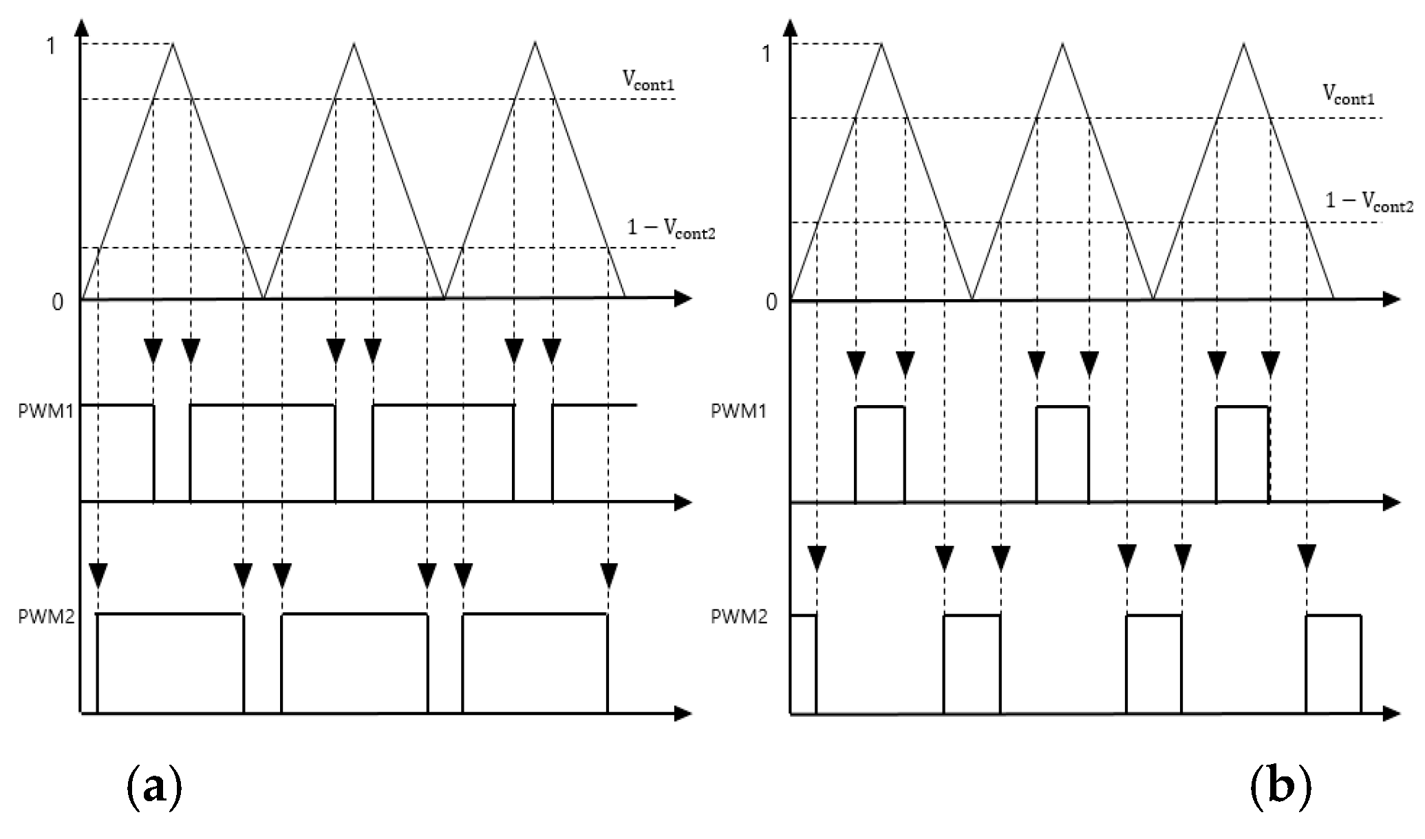
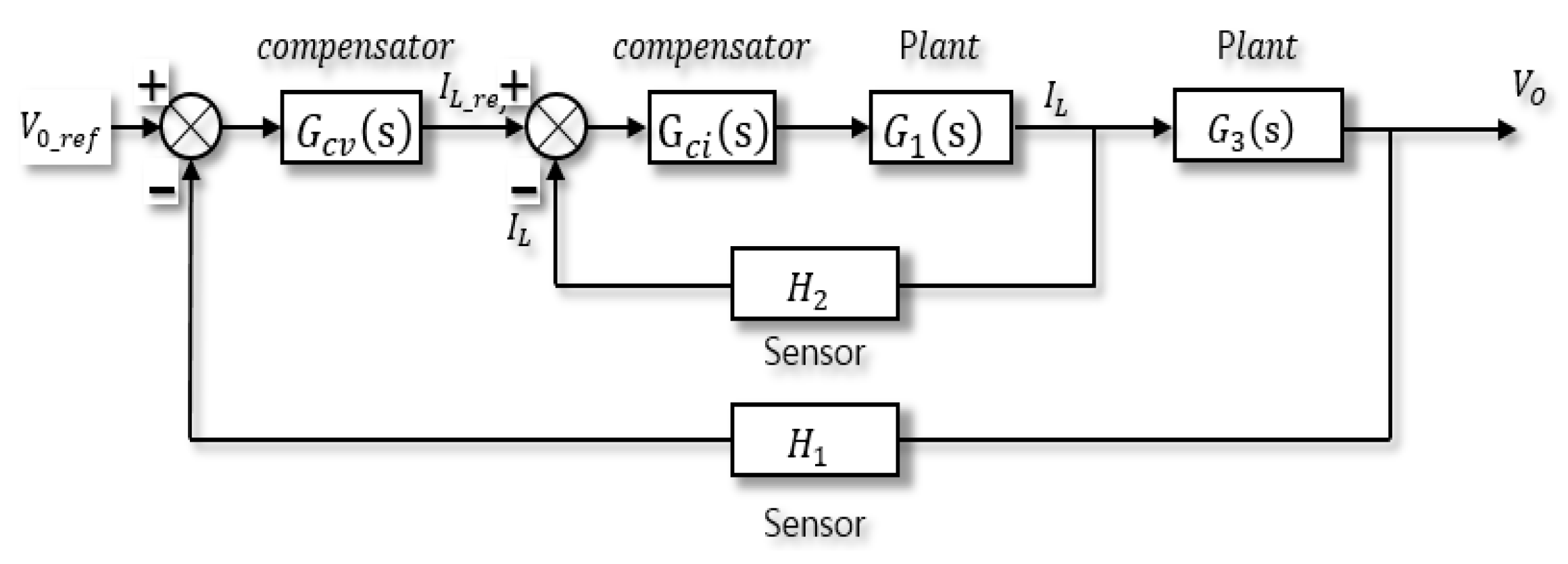
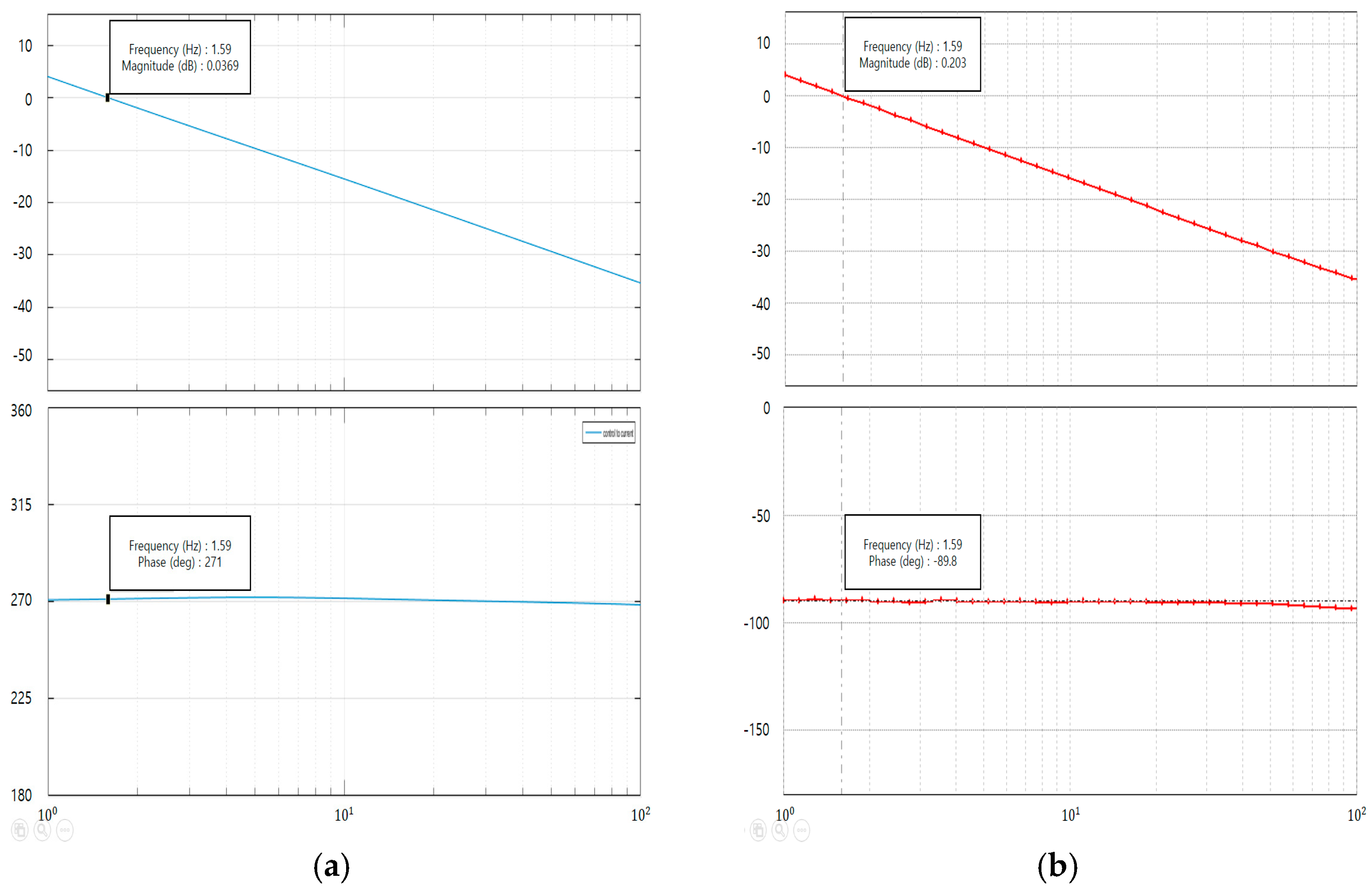
3. Controller Design

The proposed TLB controller comprises a double-loop controller, balancing controller, and PWM generator, as shown in Figure 1. The double-loop controller controls the output voltage and inductor current using a proportional-integral (PI) controller, whereas the balancing controller controls the voltage difference between the capacitors to zero through a proportional (P) controller. Each control signal determined by the two controllers generates PWM1 and PWM2 through the comparator. The PWM signals with a phase difference of 180° to activate each switch to prevent an imbalance in the capacitor voltage and to control the output voltage. The principle of PWM generation is shown in Figure 4. The PWMs of Modes 1 and 2 are shown in Figure 4a and Figure 4b, respectively.
A. 
Double-loop controller design
The double-loop controller block diagram of the TLB converter is shown in Figure 5. The output of the voltage compensator serves as the current reference, and the output of the current compensator becomes the control duty d. Block G 1 ( s ) is the transfer function of the inductor current-to-input duty; G 3 ( s ) is the transfer function of the output voltage-to-inductor current; G c v ( s ) and G c i ( s ) are the voltage and current compensators, respectively; and H 1 and H 2 are the sensor gains, which were set to one in the design. The current control loop ( T i ) and voltage control loop ( T v ) can be expressed as shown in Equations (16) and (17), respectively. To calculate T v , it is assumed that the magnitude of T i is one because G c i G 1   is much larger than one:
T i = I L ( s ) I L _ r e f ( s ) = G c i G 1 1 + G c i G 1 H 2
T v = V o ( s ) V o _ r e f ( s ) = G c v G 3 1 + G c v G 3 H 1
Each controller of the double loop uses a PI compensator with a switching frequency of 20 [kHz]. The design specifications of each compensator are listed in Table 1, where ω c is the cutoff bandwidth and PM is the phase margin. The phase margin was selected to be at least 45° considering the controller stability, and the cutoff bandwidth was selected as 1/10 of the switching frequency. Accordingly, the phase margin was set to 60° by the current controller to achieve fast response characteristics, whereas the voltage controller was set to 90° to achieve a zero overshoot. Because the switching frequency was 20 [kHz], the cutoff bandwidth for the current controller was set to 3000 [rad/s], which is less than 2 [kHz]. The cutoff bandwidth of each controller should be selected appropriately because the inner and outer loops are closely coupled when designing a double-loop controller.
Generally, the maximum cutoff bandwidth of the outer loop is set to 1/10 of the inner loop cutoff bandwidth to avoid interference between the controllers, and the interference decreases as the bandwidth separation increases. Theoretically, the bandwidth of the voltage controller is stable below 300 [rad/s], but the bandwidth separation between the controllers should be designed larger in consideration of the switching noise, unmodeled parasite elements, and parameter errors, which are not considered in the actual system. Therefore, in this study, the voltage controller bandwidth was set to less than 1/50 of the current controller’s bandwidth to guarantee a stable operation.
Based on the design goal and Equation (16), each PI controller was designed based on the following procedure: (i) the pole was added to the origin (0 Hz) to remove the steady-state error; (ii) the zero pole was added for a secure phase margin at the resonance frequency; (iii) the crossover frequency was placed at a point ten times lower than the resonant frequency to guarantee a stable operation; (iv) the DC gain was determined. The circuit parameters are listed in Table 2.
It is difficult to determine the appropriate gains of both compensators to satisfy the design specifications. SISOTOOL in MATLAB can be used to easily design compensator gains in a double-loop system. Furthermore, SISOTOOL can simultaneously display the root locus graph in the time domain and the open-loop Bode plot in the frequency domain for gains G cv ( s ) and G ci ( s ) in a double-loop system. The compensators for satisfying the design specification are expressed in Equation (18).
G cv ( s ) = 0.014191 × ( s + 31.1 ) s ,   G ci ( s ) = 0.011021 × ( s + 2134.5 ) s
The frequency response characteristics of each transfer function before and after compensation are shown in Figure 6. The frequency response of the transfer function of the inductor current to the control duty in an open loop is shown in Figure 6a. As shown, the current controller achieved a sufficient gain margin at 3000 [rad/s] and a phase margin of 60.2°, thereby satisfying the design goal. The frequency response of the output voltage to the inductor current is shown in Figure 6b.
As shown, a sufficient gain margin at 10 [rad/s] and a phase margin of 91.1° were achieved, thereby satisfying the design goal. The closed-loop response of the double-loop system, which is the step response of the output-to-reference voltage using MATLAB, is shown in Figure 7. As shown, the rising time was 0.22 [s], and a steady value was reached at 0.39 [s] and subsequently stabilized.
B. 
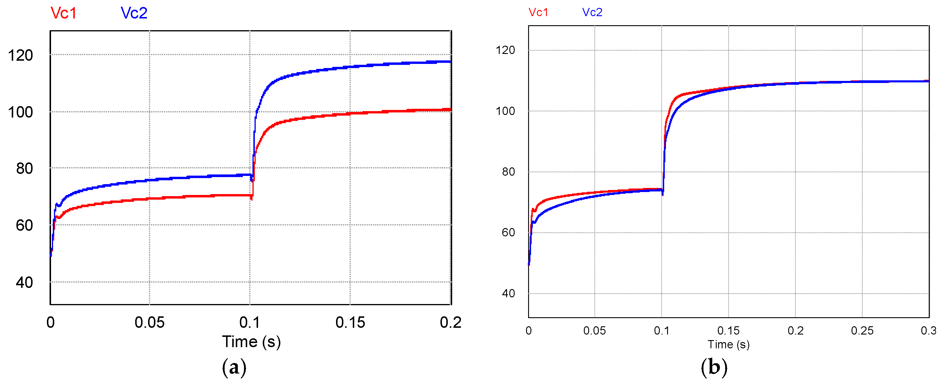
Capacitor-voltage-balancing controller design
Theoretically, the capacitor voltages v c 1 and v c 2 of the TLB converter are balanced. However, v c 1 and v c 2 are not exactly balanced in the actual applications owing to their mismatched components, such as the ESR of the capacitor or the duty difference. Therefore, capacitor-voltage-balancing controllers are essential. The average capacitor currents for one sampling period T S in Mode 1 are denoted as I C 1 T S and I C 2 T S , which are expressed in Equations (19)–(20) based on Figure 1:
I C 1 T S = v c 1 + v c 2 R + i L ( 1 v c o n t 1 )
I C 2 T S = v c 1 + v c 2 R + i L ( 1 v c o n t 2 )
Because the output of the voltage-balancing controller is Δ d , the difference between the two average capacitor currents can be obtained from Equations (19) and (20) as follows in Equation (21):
I C 1 T S I C 2 T S = i L ( v c o n t 1 v c o n t 2 ) = 2 Δ d i L
Each capacitor C 1 and C 2 can be expressed as C because its values are the same. Therefore, the transfer function for balancing the control-to-unbalancing voltage ( G Δ C ) is expressed as Equation (22):
G Δ C = Δ v c ( s ) Δ d ( s ) = 2 s C I L
where Δ v c ( s ) = v c 1 v c 2 .
Similarly, the G Δ C of Mode 2 can yield the same result as using Equation (22). The block diagram of the voltage-balancing controller is shown in Figure 8a, where a P controller is used. The closed-loop transfer function of Δ v c ( s ) can be expressed as Equation (23):
Δ v c ( s ) Δ v c r e f ( s ) = 2 k p C I L s + 2 k p C I L
where Δ v c r e f ( s ) = 0 .
Because Equation (23) describes a first-order system, the steady-state error is zero and overshoot does not occur. Therefore, the P controller can be used to balance the capacitor voltage. The design requirement is given by the cut-off bandwidth and set to ω c = 500 [rad/s]. The designed gain is K p = 0.05 by the bode diagram. The step response of the balancing controller is given in Figure 8b. It can be seen that the steady-state error is zero and there is no overshoot.

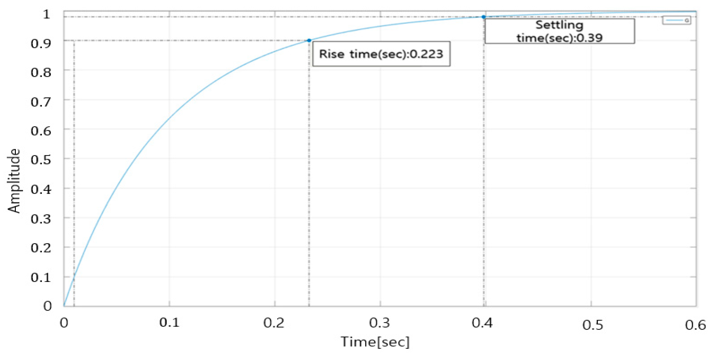
4. Simulation Results

The suggested design for the TLB controllers began with state-space averaging models. These mathematical models were converted into frequency-domain expressions and transfer functions. The controller gains were selected based on requirements, such as the cutoff frequency and phase margin. Subsequently, the frequency response was shown using the MATLAB software. The design was based on mathematical analysis instead of real hardware. Therefore, it should be verified experimentally to validate the frequency response in real circuits.
Experiments involving hardware are challenging because highly complicated experimental systems are required, e.g., a network analyzer, a high-frequency signal generator, and high accuracy measurement systems. Additionally, the correct response data are difficult to obtain because of switching noise. Hence, it is preferable to rely on circuit simulation rather than experiments to validate the design results.
Many circuit-based simulation programs are available. Among them, Powersim is a typically used software in power electronics that can perform frequency analysis from circuit drawings. In this study, the AC sweep library from Powersim was applied as the perturbation input to obtain the open-loop gain. Subsequently, the double-loop controller gains of Equation (18) were applied in the simulation. The simulation parameters used were the same as those listed in Table 2. The simulation results of MATLAB and Powersim are shown in Figure 9 and Figure 10, respectively. The open-loop gains of the voltage and current loops are shown in Figure 9 and Figure 10, respectively. Because the unit used in Powersim is “Hz,” the unit from MATLAB was converted from “rad/s” to “Hz” to match the scales. the dot marker in the Powersim plot corresponds to the frequency at which the simulation was performed.
The simulation frequency of the open-loop voltage is presented from 1 to 100 [Hz] to clearly show the response around the cutoff frequency (see Figure 9). Using MATLAB, the cutoff frequency was 1.59 [Hz], which corresponds to 10 [rad/s], and the phase margin was 90° with a 49.5 [dB] of gain margin, as shown in Figure 9a. The same cutoff frequency was obtained in Powersim with a phase margin of 90° and a gain margin of 49 [dB], as shown in Figure 9b.
A comparison of the open-loop current results is shown in Figure 10. Using MATLAB, the cutoff frequency was 478 [Hz], which corresponds to 3000 [rad/s], and the phase margin was 60° with an infinite gain margin, as shown in Figure 10a. The same cutoff frequency was obtained in Powersim with a phase margin of 60° and an infinite gain margin, as shown in Figure 10b. Hence, it is clear that the design method is effective and applicable to real circuits. The step response of the output voltage is shown in Figure 11 to verify the performance of the controller. The command was stepped up from 150 to 217 [V] and stepped down from 217 to 150 [V] to verify the controller performance when the duty crossed the mode boundary. The waveforms of the output voltage and inductor current are shown in Figure 11 using Powersim.
The step-up response from 150 to 217 [V] is shown in Figure 11a, whereas the step-down response from 217 to 150 [V] is shown in Figure 11b.
The waveforms of the output voltage and inductor current reached the steady-state value rapidly without any overshoot. It was observed that the step response of the output voltage using MATLAB matched exactly with the Powersim result by comparing Figure 7 and Figure 11. As shown, the settling time and rising times were completely matched, thereby validating the designed controller in the time domain.
The steady-state wave forms of the inductor current, output voltage, capacitor voltage, and PWM signal are plotted in Figure 12. The steady-state waveforms at 217 and 150 [V] are shown in Figure 12a and 12b, respectively. Both capacitor voltages indicated one-half the average value of the output voltage Vo, even though Vcon2 was imposed with a slight phase delay, as shown in Figure 12.
The voltage difference between vc1 and vc2 approached zero in the steady state. In addition, the inductor current had an error range within 5%, whereas the output voltage had an error range within 1% when the PWM operated at each phase difference of 180°.
The performance of the unbalancing controller is verified through PSIM simulation. The capacitance of each capacitor is set to have different values such as C 1 = 2400 and C 2 = 1800   [ u F ] . The simulation results are shown in Figure 13. The voltage unbalance that happened without the balancing controller as shown in Figure 13a. The balanced voltage is achieved with the balancing controller, as shown in Figure 13b.

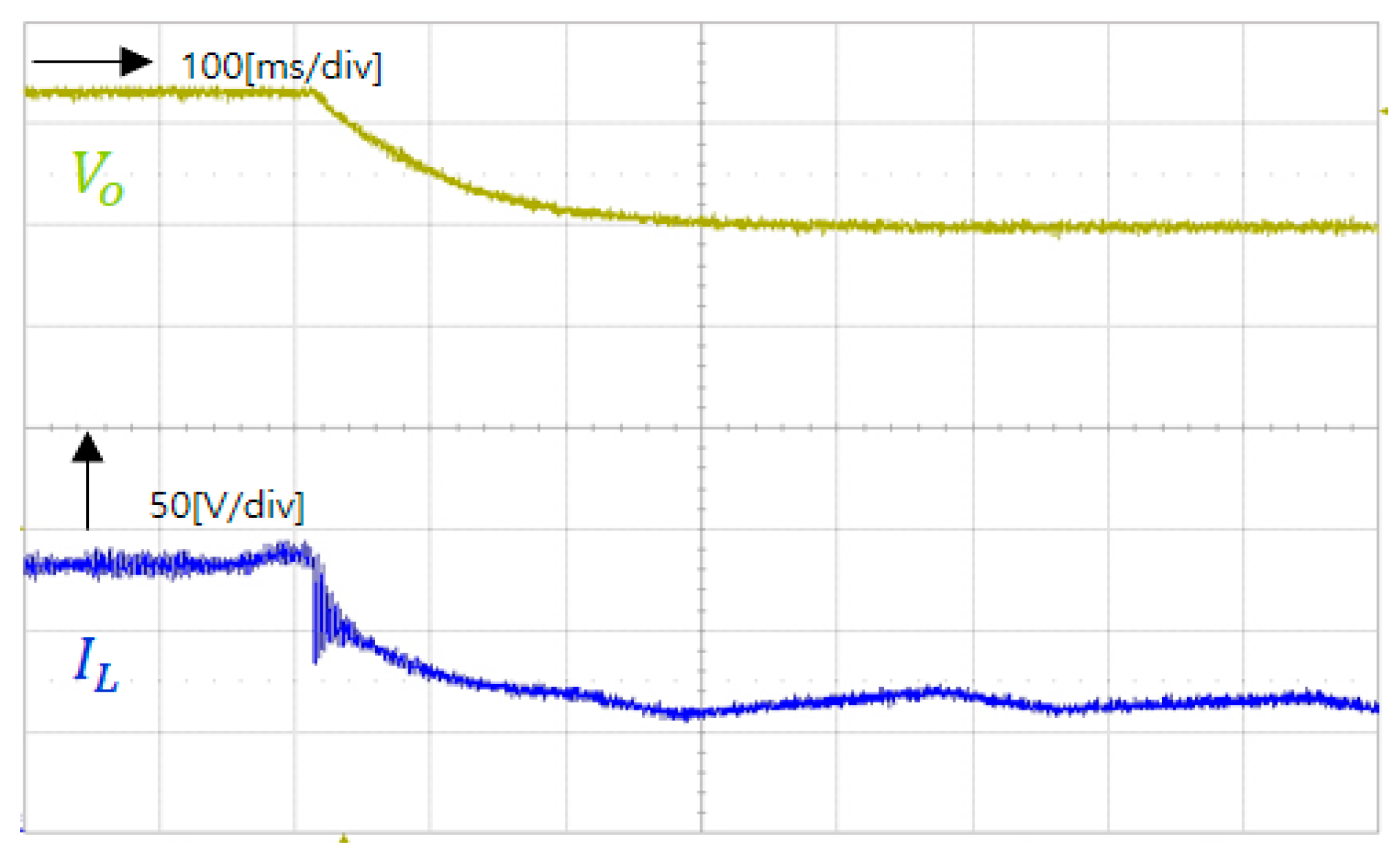
5. Experimental Validation

Experiments were conducted using a hardware setup, as shown in Figure 14, to validate the proposed modeling and controller design method. A 320F28069 DSP was used as a controller, and the experimental hardware was built using the circuit parameters shown in Table 2. A DC power supply was used for the input voltage, and measurements were performed using the same conditions as in the simulation, i.e., from 150 to 217 [V] and from 217 to 150 [V].
The experimental results for the voltage-balancing controller at 150 and 217 [V] are plotted in Figure 15 and Figure 16, respectively. Both capacitor voltages indicated one-half the output voltage Vo even though V c o n t 2 was imposed with a slight phase delay, as shown in Figure 13. The voltage difference between v c 1 and v c 2 approached zero at the steady state. The performance of the balancing controller can be proven from these figures.
The experimental results of the step response are shown in Figure 17 and Figure 18. The step-up waveform from 150 to 217 [V] is shown in Figure 17, whereas the step-down waveform from 217 to 150 [V] is shown in Figure 18. As shown in the figures, the steady-state values of the output voltage transition from 217 and 150 [V] were attained within 0.4 [s] without an overshoot, even during the mode change period. These results were almost identical to the simulation results from Powersim and MATLAB. In addition, the current waveform reached the steady state value rapidly without an overshoot, which is consistent with the results from Powersim. Hence, the controller design based on the proposed modeling method is validated.

6. Discussion

The mathematical expression of the three-level boost converter using thr unified modeling approach has been presented in the main section of the paper. In addition, the way of designing the double loop controller is shown in a step-by-step sequence.
The frequency responses of the converter using the real circuit are analyzed to prove the validity of the suggested mathematical model approaches. Since both responses are exactly the same, the proposed method is effective and definite. This process is necessary because there have not been any references or papers for the unified modeling method which can be operable for the full duty range. Therefore, it is required for the verification process of the proposed method.
The time responses for the full duty variations are obtained through computer simulations and verified from the experiments. It can be seen that the actual responses are exactly matched to the design specifications. The controller design methodology has been verified from the time response of the simulation and experimental results.
The whole design procedures and the verification methods are presented and proved to be effective in real circuits. Since the three-level boost converter is commonly used in the power converters, such as solar PCS (Power Conditioning System) and ESS (Energy Storage System), the suggested design method can be very effective in the renewable energy conversion systems.

7. Conclusions

A new modeling method for a TLB converter based on a unified modeling approach was presented herein. The state-space equations were derived from only two state variables rather than three state variables. Furthermore, the mathematical expansions proved that the unified model can be obtained regardless of the mode changes. The proposed modeling method is based on the concept that the output voltage, instead of two capacitor voltages, can be used as a new state variable. This suggests that the small-signal modeling of the TLB converter is exactly the same as that of the conventional single-level boost converter, except for the capacitance parameter. Therefore, the linear controller can be used for the double-loop configuration. A method for designing a double-loop controller based on the frequency design method with fast response characteristics without overshoot was proposed using the suggested modeling equation. The simulation and experimental results were consistent with the theoretical predictions, thereby validating the proposed modeling method and the double-loop controller designed using the suggested method. The proposed modeling and controller design methods are unique and practical; hence, they are applicable to practical systems such as solar inverters and energy-storage systems.
The parallel connection of the TLB converter can be found in the high-power applications. It is quite challenging work to design parallel-connected converters due to the circulation current of parallel converters. It is a further research topic for the parallel connected TLB converters using the unified approach.

Author Contributions

Writing—original draft, K.-M.L.; Project administration, I.-S.K. All authors have read and agreed to the published version of the manuscript.

Funding

This research was supported by National Research Foundation of Korea (201800870005) and Technology Innovation Program (201801170005) by the MOTIE, Korea.

Institutional Review Board Statement

Not applicable.

Informed Consent Statement

Not applicable.

Data Availability Statement

Not applicable.

Acknowledgments

The authors acknowledge all the participants in the study.

Conflicts of Interest

The authors declare no conflict of interest.

Nomenclature

v o ( t ) Output voltage, Sum of capacitor voltages
v c 1 ( t ) Capacitor 1 voltage
v c 2 ( t ) Capacitor 2 voltage
C t Series capacitance of C 1 and C 2   ( C t = C 1 C 2 C 1 + C 2 )
r L Inductor resistance
L Inductance
R Load resistance
d ( t ) Duty ratio
i L ( t ) Inductor current
v i n Input voltage
i ^ L ( t ) Small signal of inductor current
v ^ o ( t ) Small signal of output voltage
d ^ ( t ) Small signal of duty ratio
I L Steady-state value of inductor current
V o Steady-state value of output voltage
D Steady-state value of duty ratio
G 1 ( s ) Control-to-current transfer function
G 2 ( s ) Control-to-voltage transfer function
G 3 ( s ) Current-to-voltage transfer function
G Δ C ( s ) Control-to-unbalancing function
G cv ( s ) Voltage controller
G ci ( s ) Current controller
ω c Cutoff bandwidth
PMPhase margin

References

  1. Erickson, R.W.; Maksimovic, D. Fundamentals of Power Electronics, 2nd ed.; Kluwer: Norwell, MA, USA, 2001. [Google Scholar]
  2. Barazarte, R.Y.; González, G. Design of a Two-Level Boost Converter. In Proceedings of the Eleventh LACCEI Latin American and Caribbean Conference for Engineering and Technology, Boca Raton, FL, USA, 16 August 2013; pp. 1–8. [Google Scholar]
  3. Kim, S.-H.; Cha, H.-N.; Kim, H.-G.; Choi, B.-C. Clamp-mode Three-level High Voltage Gain Boost Converter using Coupled Inductor. Korean Inst. Power Electron. 2012, 17, 500–506. [Google Scholar] [CrossRef] [Green Version]
  4. Zhao, Q.; Lee, F.C. High-Efficiency, High Step-Up DC-DC Converters. IEEE Trans. Power Electron. 2003, 18, 65–73. [Google Scholar] [CrossRef] [Green Version]
  5. Li, W.; He, X. Review of Nonisolated High-Step-Up DC/DC Converters in Photovoltaic Grid-Connected Applications. IEEE Trans. Ind. Electron. 2011, 58, 1239–1250. [Google Scholar] [CrossRef]
  6. Palma, L.; Todorovic, M.H.; Enjeti, P.N. A high gain transformer-less DC-DC converter for fuel-cell application. In Proceedings of the IEEE 36th Power Electronics Specialists Conference, Dresden, Germany, 16 June 2005; pp. 2514–2520. [Google Scholar]
  7. Ismail, E.H.; Al-Saffar, M.A.; Sabzali, A.J. High conversion ratio dc–dc converters with reduced switch stress. IEEE Trans. Circuits Syst. I Regul. Pap. 2008, 55, 2139–2151. [Google Scholar] [CrossRef]
  8. Wai, R.-J.; Duan, R.-Y. High step-up converter with coupled-inductor. IEEE Trans. Power Electron. 2005, 20, 1025–1035. [Google Scholar] [CrossRef]
  9. Shen, M.; Peng, F.Z.; Tolbert, L.M. Multilevel dc-dc power conversion with multiple dc sources. IEEE Trans. Power Electron. 2008, 23, 420–426. [Google Scholar] [CrossRef]
  10. Kim, C.M.; Kim, J.S. Comparative Analysis of Efficiency and Power Density of Single-Phase and 3-Level Boost Converters for PV System. Korean Inst. Power Electron. 2020, 25, 127–132. [Google Scholar]
  11. Zhang, M.T.; Jiang, Y.; Lee, F.C.; Jovanovic, M.M. Single-phase three-level boost power factor correction converter. In Proceedings of the 10th Annual Applied Power Electronics Conference and Exposition, Dallas, TX, USA, 5–9 March 1995; pp. 434–439. [Google Scholar]
  12. Chen, H.C.; Lin, W.J. MPPT and Voltage Balancing Control with Sensing Only Inductor Current for Photovoltaic-Fed, Three-Level, Boost-Type Converters. IEEE Trans. Power Electron. 2014, 29, 29–35. [Google Scholar] [CrossRef]
  13. Yaramasu, V.; Wu, B. Three-level boost converter based medium voltage megawatt PMSG wind energy conversion systems. In Proceedings of the IEEE Energy Conversion Congress and Exposition, Phoenix, AZ, USA, 17–22 September 2011; pp. 561–567. [Google Scholar]
  14. Lin, B.-R.; Lu, H.-H. A novel PWM scheme for single-phase three level power-factor-correction circuit. IEEE Trans. Ind. Electron. 2000, 47, 245–252. [Google Scholar]
  15. Wu, H.; He, X. Single phase three-level power factor correction circuit with passive lossless snubber. IEEE Trans. Power Electron. 2002, 17, 946–953. [Google Scholar]
  16. Lee, M.; Kim, J.-W.; Lai, J.-S. Small-signal Modeling of Three-Level Boost Rectifier and System Design for Medium-Voltage Solid-State Transformer. In Proceedings of the 2019 10th International Conference on Power Electronics and ECCE Asia, Busan, Republic of Korea, 27–30 May 2019. [Google Scholar]
  17. Kwon, J.M.; Kwon, B.H.; Nam, K.H. Three-Phase Photovoltaic System with Three-Level Boosting MPPT Control. IEEE Trans. Power Electron. 2008, 23, 2319–2327. [Google Scholar] [CrossRef] [Green Version]
  18. Lee, M.; Kim, J.-W.; Lai, J.-S. Derivation of CCM/DCM boundary and Ideal Duty-Ratio Feedforward for Three-level boost Rectifier. In Proceedings of the IEEE Applied Power Electronics Conference and Exposition (APEC), Anaheim, CA, USA, 17–21 March 2019; pp. 1173–1179. [Google Scholar]
  19. Chen, H.-C.; Liao, J.-Y. Design and Implementation of Sensorless Capacitor Voltage Balancing Control for Three-Level Boosting PFC. IEEE Trans. Power Electron. 2014, 29, 3808–3817. [Google Scholar] [CrossRef] [Green Version]
  20. Kim, J.; Yang, O. Three-Level Boost Converter Design for High Efficiency Photovoltaic Power Conditioning System. Adv. Sci. Technol. Lett. 2014, 51, 68–72. [Google Scholar]
  21. Zhao, E.; Han, Y.; Lin, X.; Liu, E.; Yang, P.; Zalhaf, A.S. Harmonic characteristics and control strategies of grid-connected photovoltaic inverters under weak grid conditions. Int. J. Electr. Power Energy Syst. 2022, 142 Pt B, 142. [Google Scholar] [CrossRef]
  22. Zhao, E.; Han, Y.; Lin, X.; Yang, P.; Blaabjerg, F.; Zalhaf, A.S. Impedance characteristics investigation and oscillation stability analysis for two-stage PV inverter under weak grid condition. Electr. Power Syst. Res. 2022, 209, 108053. [Google Scholar] [CrossRef]
Figure 1. The proposed controller configuration of the TLB converter.
Sustainability 15 01597 g001
Figure 2. Operational waveforms of TLB converter: (a) Mode 1 [duty > 0.5], (b) Mode 2 [duty < 0.5].
Sustainability 15 01597 g002
Figure 3. Operation circuit of TLB converter. (a) Mode 1 [duty > 0.5]. (b) Mode 2 [duty < 0.5].
Sustainability 15 01597 g003
Figure 4. Operation of comparator. (a) Mode 1 (b) Mode 2.
Sustainability 15 01597 g004
Figure 5. Block diagram of double-loop control.
Sustainability 15 01597 g005
Figure 6. Bode diagram of TLB (by MATLAB). (a) control-to-current transfer function (b) current-to-output transfer function.
Sustainability 15 01597 g006
Figure 7. Step responses of voltage output (by MATLAB).
Sustainability 15 01597 g007
Figure 8. Balancing voltage controller characteristics. (a) Controller configuration (b) Step response.
Sustainability 15 01597 g008
Figure 9. Comparison of open-loop voltage Bode plots [1–100 Hz]. (a) MATLAB (b) Powersim.
Sustainability 15 01597 g009
Figure 10. Comparison of open-loop current Bode plots [100–10 kHz]. (a) MATLAB (b) Powersim.
Sustainability 15 01597 g010
Figure 11. Waveform of step response. (a) 150 to 217 V (b) 217 to 150 V.
Sustainability 15 01597 g011
Figure 12. Steady-state waveforms. (a) at 217 V (b) at 150 V.
Sustainability 15 01597 g012
Figure 13. The performance of the balancing controller. (a) Without balancing controller (b) With balancing controller.
Sustainability 15 01597 g013
Figure 14. Experimental setup.
Sustainability 15 01597 g014
Figure 15. Vc at 217 [V].
Sustainability 15 01597 g015
Figure 16. Vc at 150 [V].
Sustainability 15 01597 g016
Figure 17. Voltage and current waveforms at 217 [V].
Sustainability 15 01597 g017
Figure 18. Voltage and current waveforms at 150 V.
Sustainability 15 01597 g018
Table 1. The specification of controller.
SymbolQuantityValue
Voltage compensator
ω c Cutoff bandwidth10 [rad/s]
PMphase margin90 [deg]
Current compensator
ω c Cutoff bandwidth3000 [rad/s]
PMphase margin60 [deg]
Table 2. Circuit Parameter for the simulation.
ParameterQuantityUnit
V o Output voltage217 [V]
V i n Input voltage100 [V]
r L Inductance ESR0.3 [ Ω ]
L Inductance1.0 [mH]
C 1 Capacitance11200 [ μ F]
C 2 Capacitance21200 [ μ F]
f s w Switching frequency20 [kHz]
Disclaimer/Publisher’s Note: The statements, opinions and data contained in all publications are solely those of the individual author(s) and contributor(s) and not of MDPI and/or the editor(s). MDPI and/or the editor(s) disclaim responsibility for any injury to people or property resulting from any ideas, methods, instructions or products referred to in the content.

