Article

Slot-Die Coated Copper Indium Disulfide as Hole-Transport Material for Perovskite Solar Cells

by
Sajjad Mahmoodpour
1,
Mahsa Heydari
1,
Leyla Shooshtari
1,
Rouhallah Khosroshahi
1,
Raheleh Mohammadpour
1,* and
Nima Taghavinia
1,2,*
1
Institute for Nanoscience and Nanotechnology, Sharif University of Technology, Tehran 14588-89694, Iran
2
Nanoparticles and Coating Lab, Department of Physics, Sharif University of Technology, Tehran 14588-89694, Iran
*
Authors to whom correspondence should be addressed.
Sustainability 2023, 15(8), 6562; https://doi.org/10.3390/su15086562
Submission received: 26 February 2023 / Revised: 8 April 2023 / Accepted: 11 April 2023 / Published: 12 April 2023
(This article belongs to the Special Issue Toward Cost-Effective and Efficient Alternatives to Si Photovoltaics)

Abstract

:
Perovskite photovoltaics have the potential to significantly lower the cost of producing solar energy. However, this depends on the ability of the perovskite thin film and other layers in the solar cell to be deposited using large-scale techniques such as slot-die coating without sacrificing efficiency. In perovskite solar cells (PSCs), Spiro-OMeTAD, a small molecule-based organic semiconductor, is commonly used as the benchmark hole transport material (HTL). Despite its effective performance, the multi-step synthesis of Spiro-OMeTAD is complex and expensive, making large-scale printing difficult. Copper indium disulfide (CIS) was chosen in this study as an alternative inorganic HTL for perovskite solar cells due to its ease of fabrication, cost-effectiveness, and improvements to the economic feasibility of cell production. In this study, all layers of perovskite solar cell were printed and compared to a spin-coating-based device. Various parameters affecting the layer quality and thickness were then analyzed, including substrate temperature, print head temperature, printing speed, meniscus height, shim thickness, and ink injection flow rate. The small print area achieved spin-coating quality, which bodes well for large-scale printing. The printed cell efficiencies were comparable to the reference cell, having a 9.9% and 11.36% efficiency, respectively.

1. Introduction

Perovskite solar cells (PSCs) have recently gained significant attention due to their remarkable improvement in power conversion efficiency (PCE), which has increased to 25.5% from 3.8% [1,2,3,4]. This rapid increase is attributed to the unique optoelectronic properties of perovskite, including long carrier lifetime, low exciton binding energy, and significant absorption coefficient [5,6,7,8,9,10]. The structure of PSCs consists of an electron layer (ETL), a perovskite (PVK) layer, and a hole transport layer (HTL); the HTL is responsible for hole transport and protection of the PVK from water and oxygen in the n-i-p configuration. Although utilizing organic transport materials, such as Spiro-OMeTAD (2,2′,7,7′-tetrakis(N,N-di-pmethoxyphenylamine)-9,9′-spirobifluorene), PTAA poly(triarylamine), or P3HT poly(3-hexylthiophene), can lead to efficient PSCs, their use is limited by the stability of the devices and their prohibitive cost; these limitations seriously hinder the commercialization of PSCs [11]. Some recent works proposed using TL-free PSCs as a easily processed and cost-effective means of meeting these commercial requirements [12].
Utilizing inorganic hole transport materials (HTMs) is a potential strategy to improve two critical parameters in the industrialization process. This approach offers several advantages, including large-hole mobility, high stability, and low-cost fabrication. Some inorganic HTMs used in PSCs include CuCrO2 [13], CuSCN [14], CuGaO2 [15], Cu2ZnSnS4 (CZTS) [16], and CuInS2 (CIS) [17]. With its chalcopyrite structure, CIS is a member of the non-toxic I-III-VI group of semiconductors. It boasts impressive properties such as a direct band gap of roughly 1.5 eV, an absorption coefficient of 105 cm−1 within the visible spectrum, and exceptional electrical and thermal stability. Whilst the electronic properties of doped spiro-OMeTAD enable high-efficiency devices in a research environment, its stability represents a major barrier. The performance of PSCs using doped spiro-OMeTAD HTLs has been shown to degrade rapidly at temperatures as low as 85 °C, while most perovskites and other PSC components are thermally stable in this range [18]. The printed CIS ink has good thermal stability because of its inorganic nature. These properties make CIS a suitable candidate for use in solar cell structures [19,20]. However, it should be noted that devices using inorganic HTLs generally are less efficient than those based on organic HTLs, such as Spiro-OMeTAD; CIS is no exception to this rule.
Several deposition techniques for creating CIS films include sputtering, chemical spray pyrolysis, electrodeposition, evaporation, and printing [21,22,23,24,25]. To commercialize device fabrication, non-vacuum techniques, particularly printing, are more favorable due to their simplicity, low-temperature processing, and efficient material consumption (nearly 100%). Slot-die coating has garnered considerable interest as a printing method due to its versatility in large-scale production utilizing roll-to-roll or sheet-to-sheet processes and its ability to handle inks with viscosities spanning from 10−3 to 103 Pa.s. This method involves injecting the proper solution through a slot in the machine head and then coating the solution. The height of the head and substrate must be fixed; the capillary force then transfers the solution with the appropriate viscosity at a constant speed [26,27,28]. Thus, by adjusting various coating parameters, such as the distance between the head and substrate, ink viscosity, and head speed, the slot-die coating method enables precise control over the film thickness. Additionally, this method is well-suited for depositing the PVK layer and all layers in the PSCs structure, making it a powerful tool for depositing these layers for both small and large-scale PSCs.
Cai et al. developed PSC modules with dimensions of 5 cm × 5 cm, achieving a PCE of around 10.6% [29]. Zuo et al. reported fully slot-die-coated PSCs with modified PEDOT; in this study, PSS was the HLT and had a PCE of 15.57% [30]. Geo et al. established PSCs through the layer-by-layer slot-die coating, using SnO2/perovskite/Spiro-OMeTAD films to achieve the highest efficiency of 14.55% [31]. Developing the HTL on the PVK through slot-die coating in PSCs is crucial, especially for large-scale devices. For instance, a large-area PSC module measuring 12.5 cm × 13.5 cm was fabricated through the partial slot-die coating of the perovskite and HTL layer on the initial substrate, which measured 15.2 cm × 15.2 cm. This configuration achieved a PCE of more than 10% [32]. A highly efficient PSC module with dimensions of 5 cm × 5 cm was reported by using a facile approach for HTL deposition through the slot-die coating, with a PCE of 17.7% [33]. Seok-In Na et al. investigated the effect of different solvents, finding that the best PSC, based on optimized slot-die coating parameters, had an efficiency of 15.4% and a substrate dimension of 2.5 cm × 2.5 cm [34].
While achieving the inorganic HTL through the slot-die coating process is a valuable goal for commercializing PSCs, there is no clear report on depositing Cu-based inorganic layers via the slot-die coating process. Most reports focus on the slot-die coating of the NiO HTL as the inorganic layer in PSCs with the p-i-n structures [35]. In this study, we designed the n-i-p structure of a small PSC by partially slot-die coating the CIS as the HTL of the PSC structure. We then fabricated a fully PSC-based slot-die coating by depositing TiO2/PVK/CIS through an in-house assembled slot-die machine. It is worth noting that the physical properties of the ink solution, such as viscosity, boiling point, and surface tension, significantly affect film formation during the slot-die process. As the drying time of the ink required to prepare a homogeneous and compact film during the slot-die coating process is longer than spin-coating [36], access to high-quality HTL films based on common HTL inks is limited. The literature reveals a diversity of organic solvents, such as chlorobenzene (CB) solvent, chloroform, ethyl acetate (EA), acetone, tetrahydrofuran (THF), etc., used to effectively deposit the HTL [37]. However, most published studies focus on spin-coating methods for small-scale PSCs and there is still a lack of information about morphology control of the HTL based on the organic solvent used in slot-die coating.
This research employed large-scale production methods to create a perovskite solar cell. Slot die coating is a process used to produce thin and uniform films, commonly used in applications where the precise coating is required. A key concern in this process is determining the appropriate operating limits for various parameters, such as coating speed, flow rate, vacuum pressure, coating gap, liquid viscosity, and surface tension [38]. In this research, the slot die method was used to label all layers of the perovskite cells. The study found that slot-die technology enables precise, repeatable, and scalable deposition of liquid thin films of ETL, PVK, and HTL. The slot-die head is considered the technology’s core because its design extensively affects the layer quality. One of the main advantages of using the slot die coating technique is the chance to scale up the process from a lab scale to an industrial one. This technique has the most promising score for ink printing in printed electronics [37]. Other parameters, such as ink concentration and rheology, printing speed, substrate temperature, injection head temperature, ink injection speed, distance from the edge of the head to the substrate, injection head geometry, and protective atmosphere, are also considered as influencing variables. Four types of printing solutions were used for titanium oxide blocking, mesoporous titania, three-cation perovskite, and CIS as the hole-transporting layer. By printing the CIS layer as a hole transport material and comparing it with the spin-coated layer, the researchers analyzed the CIS printing capability by changing various parameters affecting the quality and thickness of the layer. The study achieved a maximum efficiency of 9.38% by utilizing the slot-die printing method, which was comparable to the spin-coating method and showed the potential for employing CIS as an inorganic HTL for large-scale PSC. The use of slot-die printing is a crucial method as it minimizes the amount of precursors and waste material, which is the goal of sustainability.

2. Experimental Section

2.1. Materials

Fluorine-doped tin oxide (FTO) glass substrates (Sigma-Aldrich, Saint Louis, MO, USA, TEC-7 Ω sq), titanium dioxide paste (TiO2-30 NRD) from IRASOL, lead iodide (PbI2) from IRASOL, formamidinium iodide (FAI) and methylammonium bromide (MABr) from Greatcell Solar, lead bromide (PbBr2) from IRASOL, and cesium iodide (CsI) 99.99%, N–N dimethylformamide (DMF), dimethyl sulfoxide (DMSO), chlorobenzene (CB), 2-propanol (IPA), and acetonitrile from Sigma-Aldrich, CIS (IRASOL), were used to create the device.

2.2. Device Fabrication

2.2.1. Fabrication of Spin Coating-Based Devices

Fluorine-doped Tin Oxide (FTO) substrates (Sigma-Aldrich, TEC-7 Ω sq−1) were etched by zinc powder and hydrochloric acid solution. The cleaning process was completed by using de-ionized water, ethanol, and 2-propanol for 10 min. FTO glasses were heated at 500 °C in the furnace and treated under UV-ozone for 15 min. A 50 nm-thick compact TiO2 (c-TiO2) layer (250 µL) was deposited onto the FTO by the spin coating method previously reported by our group [39] and for 30 min heated at 500 °C. A mesoporous TiO2 layer was deposited on the c-TiO2 by using a 1:6 w/w diluted paste (IRASOL) in ethanol (30 µL) via spin coating for 20 s at 4000 rpm and was sintered for 30 min at 450 °C. The 3D mixed cation/anion solution was then prepared by a solution containing FAI (1.5 M), CsI (0.05 M), PbI2 (1.5 M), MABr (0.2 M), and PbBr2 (0.22 M) in anhydrous DMF: DMSO solvent (4:1 vol ratio). The perovskite solution (30 µL) was spin-coated in a two-step program for 10 s at 1000 rpm and for 20 s 6000 rpm, respectively. During the last 5 s of the second step, the chlorobenzene was poured on the substrate while spinning to form the perovskite nuclei (250 µL). After perovskite deposition, the substrates were annealed for 1 h at 100 °C. CIS was then deposited for 10 s at 3000 rpm for 2 steps (each time 60 µL) to gain a suitable thickness. Finally, the Carbon paste (IRASOL) was bladed on the substrates and annealed for 30 min at 100 °C.

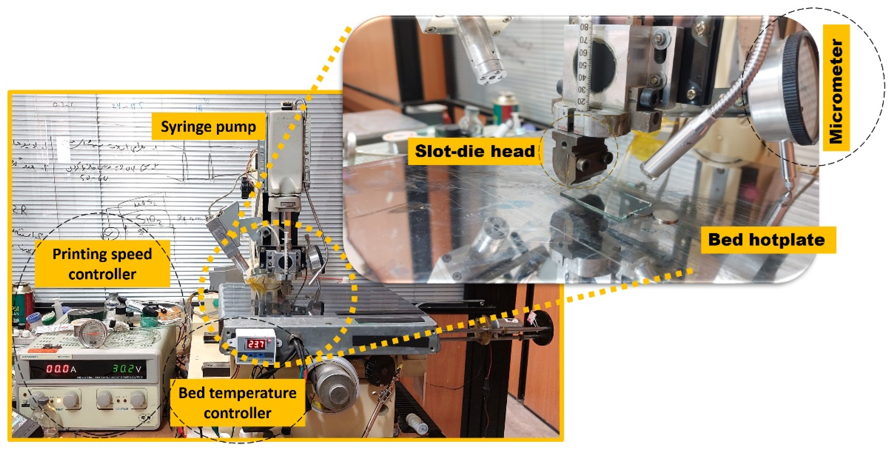
2.2.2. Fabrication of Slot-Die Printed Devices

To create the TiO2 precursor solution, 369 µL of titanium tetraisopropoxide (Merck, Darmstadt, Germany, 99.99%) and 35 µL of 2 M HCl (Merck) were dissolved in 5.06 mL of 99.9% anhydrous ethanol (Merck). The solution was then applied to clean FTO (Florine doped Tin oxide) substrates using a slot-die coater and annealed at 500 °C for one hour. After that, the TiO2 nanoparticle paste (IRASOL-PST-20) was diluted with anhydrous ethanol at a ratio of 1:5.5 wt% and then slot-die coated onto the FTO/compact TiO2 layers. For the next step, a mixed-cation mixed-halide perovskite (Cs0.05(MA0.17FA0.83)0.95Pb(I0.83Br0.17)3) absorber layer was deposited on top of the FTO/compact-TiO2/mesoporous-TiO2 substrates via one-step slot-die deposition. To create the perovskite precursor solution, 1.5 mmol of PbI2 (IRASOL), 1.5 mmol of PbBr2 (IRASOL), 1 mmol of Formamidinium Iodide (FAI, Dyesol), and 1 mmol of Methylammonium Bromide (MABr, Dyesol) were dissolved in 1 mL of anhydrous DMF:DMSO (4:1; v/v) (Merck). We then added 50 µL of CsI (Sigma, Tokyo, Janpan, 99%) solution (CsI dissolved in 1.5 M DMSO) to 950 µL. The perovskite precursor solution was applied to the FTO/compact-TiO2/mesoporous-TiO2 substrates using the slot-die coater at a speed of 5 mm/s and a gap of 200 μm at 35 °C. The coated layer was transferred to a vacuum chamber at 6 Pascal pressure and subsequently transferred to a hotplate for 10 min at 100 °C in ambient air after the first color change. To create the hole transport layer, a 25 mg/mL copper indium disulfide (CIS) precursor solution (Sharif solar) dispersed in chloroform (Merck) was used. Our research team constructed a custom slot-die machine, as shown in Figure 1, featuring a motorized X-Y table, syringe pump, and heated bed with a specific heating element for temperature control. The X-Y table was exceptionally stable, allowing for precise printing. All layers were printed by slot-die coater equipped with a roller except the top electrode. The carbon paste was deposited by blade coating. For patterning, we used a screen with a strip-type pattern. In this experiment, we used the 80 × 30 mm FTO substrate. As some ink is accumulated at the start and finish regions of printing, as well as on the printing head, the estimated ink consumption is not accurate. The average amount of ink consumption in each step was declared as follows: the TiO2 blocking layer was less than 1.16 µL/cm2;TiO2 meso was less than 0.31 µL/cm2; PSK ink was: 0.41 µL/cm2; and CIS was 1.25 µL/cm2. For more precise measurement of ink consumption, it may be possible to use gravimetric measurement on substrate with and without the deposited layer by a six-zero scale by eliminating the start and finish sides of the printed area.

2.3. Characterization

The layers’ surface topography and cross-sectional images were investigated using a field-emission scanning electron microscope (FE-SEM, TESCAN, Mira 3-XMU, Kohoutovice, Czech Republic) equipped with an energy-dispersive X-ray spectroscopy (EDS) analyzer. VEECO-CP Research and DME scanners were used for atomic force microscopy analysis. The X-ray diffraction patterns were measured with a PANalytical X’Pert Pro MPD X-ray diffractometer with Cu Kα radiation (λ = 0.15406 nm). The UV-Vis transmission spectra of the layers were recorded using a Perkin-Elmer 950 spectrometer in the 350−900 nm wavelength range. The solar cells were illuminated with a solar simulator (IRASOL SIM-1020 system) equipped with an AM 1.5G filter, providing 100 mW·cm−2 of illumination, and calibrated using a Si photodiode. The J-V characteristics were obtained at a scan rate of 5 mV·s−1 under the AM1.5G spectrum using the Palm Sens potentiostat source meter. Steady-state photoluminescence (PL) spectra were recorded using an Avantes TEC-2048 (Apeldoorn, The Netherlands) spectrometer with a diode laser (λ = 450 nm) for illumination and photon collection from the glass side. The incident-photon-to-current efficiency (IPCE) test was performed using the IRASOL IPCE tester.
We designed the slot-die coater concept and had it machined and fabricated by Sadra Instruments. To enable precise movement and X-Y control, an old metallography microscope was adapted for printing requirements by installing a motorized X-Y table and a high-precision temperature-controlled bed. This experiment’s system is the fourth optimized system fabricated to minimize backlash and unwanted vibrations during the printing process. The isometric view of the 10 cm width slot-die mold can be seen in Figure S1.

3. Results

This research targeted a fully printed perovskite solar cell; thus, all thickness and film quality parameters are explicitly optimized for each layer according to optimized spin-coated parameters.

3.1. TiO2 as Electron Blocking Layer

In the first step, the effect of the temperature on the block layer morphology was assessed. TiO2 block solution was printed at room temperature of 20 °C and a slightly higher temperature of 25 °C. The printing parameters for the printing blocking layer are indicated in Table 1. A temperature slightly higher than room temperature was chosen to form a layer with a more suitable morphology. The layer formed at higher temperatures was expected to prevent moisture condensation during deposition [40]. However, as shown by the AFM microscope images in Figure 2a,b, increasing the deposition temperature increased surface roughness from 16 nm to 23 nm at 20 °C and 25°C, respectively. Therefore, room temperature was used to deposition the TiO2 blocking layer for the next set of fabricated solar cells. To achieve the same thickness as that obtained in the spin-coated layer (approximately 50 nm, as shown in Figure S3), different deposition steps (two layers, four layers, and six layers) and printing speeds (1 mm/s, 2 mm/s, 3 mm/s, and 4 mm/s) were tested. As indicated in Figure 2c, the thickness of the block layer changed from 47 to 51 nm by varying printing speeds and deposition steps. Based on the results, the optimum thickness was obtained at 3 mm/s for printing four layers of block solution. It should be noted that, in this step, the block solution was used in the same concentration as the spin-coated layer. If block solution engineering is undertaken, the desired thickness can be achieved with reduced layer printing. Transmittance data for the printed layers can be seen in Figure S3.

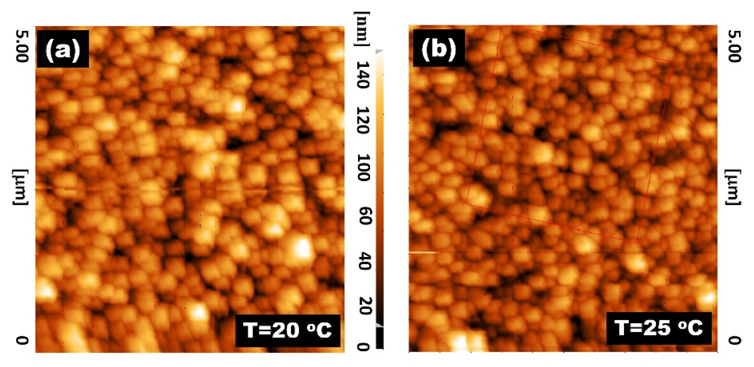
3.2. TiO2 as the Mesoporous Layer

To optimize the thickness of the mesoporous titanium dioxide mp-TiO2 layer, the effect of gap distance, printing speed, and substrate temperature on the thickness of the printed layer was investigated. As can be seen in Figure 3a, the gap distances of 100, 200, 300, and 400 um were applied for mp-TiO2 deposition. The obtained thicknesses were around 210 nm, which lies in the range of spin-coated mp-TiO2 thin film (250 nm). To tune the proper thickness based on the spin-coated film thickness, printing speeds of 1.5 to 12 mm/s at a fixed gap distance of 200 um were tested, with the thickness changing from 180 to 250 nm (Figure 3b). Although both speeds of 1.5 and 11 mm/s showed a thickness of about 250 nm, the printed layer with a higher speed had a more uniform appearance; thus, this speed was chosen as the optimum printing speed. The printing of the mp-TiO2 solution was then carried out at temperatures ranging from 22 °C to 60 °C, with an optimized printing speed of 11 mm/s and a gap of 200 μm. These parameters were carefully selected to achieve the appropriate thickness, optimized by spin coating. The impact of temperature on the thickness of the printed layer is shown in Figure 3c. As shown, an increase in temperature results in an increase in the thickness of mp-TiO2. However, the thickness deviates significantly from its optimum value at higher temperatures. As the substrate temperature increases, the viscosity of the ink being printed decreases, making it easier for the material to flow and spread out on the substrate. This can result in a thicker printed layer, as shown in Figure 3b. Based on the results, the suitable substrate temperature was obtained at 42 °C. Figure 3d displays surface FESEM images of a mp-TiO2 film.

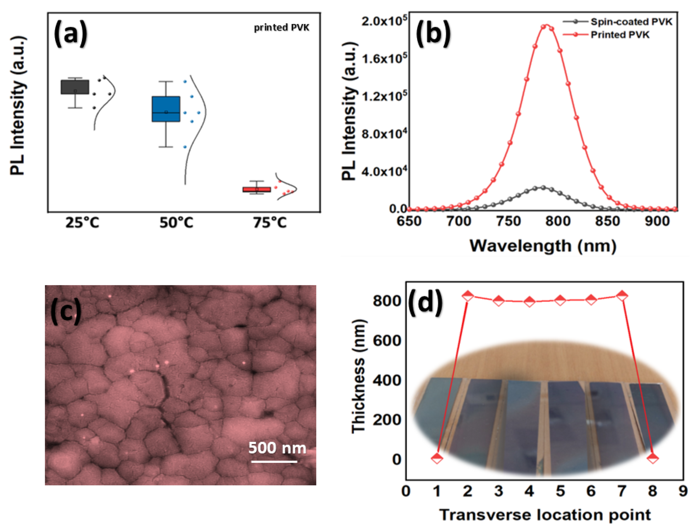
3.3. Perovskite Layer

In this step, we investigated critical factors for pinhole-free polycrystalline perovskite thin films and thickness control, such as gap distance, printing speed, and substrate temperature, using optical measurements. To begin, we analyzed the effect of gap distance. As shown in Figure 3a, there was no significant change (from 790 to 810 nm) in the thickness of the perovskite layer. Therefore, we selected the median 200 µm gap as it efficiently controlled the liquid bank under the printing head. Next, we examined the effect of different printing speeds at the fixed gap distance (200 um) to determine the minimum thickness. The impact of printing speed on the layer thickness is shown in Figure 3b. We found that lower speeds resulted in higher thicknesses, and this regime gradually changed at higher speeds by entering the landau-Levich regime. It’s worth noting that the perovskite film is susceptible to humidity and temperature, and the solvent removal procedure is critical. To address this, we used two approaches. The first approach is the vacuum-assisting method, in which the substrate is quickly transferred to the vacuum chamber at 6-pascal pressure after printing the perovskite solution. The second approach involves using an anti-solvent. In the case of the usual vacuum-based perovskite phase change process, the substrate temperature should be between 35 and 45 °C to ensure suitable substrate wetting. However, an increase in substrate temperature is not necessary for the perovskite we use and when using ethyl acetate as an anti-solvent to form the perovskite phase. In fact, in the case of using anti-solvent, the photoluminescence decreased by temperature increment (Figure 4a).
Figure S4a,b shows the absorbance data and appearance changes in perovskite thin films when varying the substrate temperature. Based on our observations, the surface appearance of anti-solvent-based perovskite thin films is much shinier than vacuum-based thin films, indicating improved crystallinity. The higher photoluminescence (PL) peak intensity of anti-solvent-based thin films than vacuum-based ones confirms this finding (Figure S5a). Consequently, the anti-solvent method was selected for fabricating fully printed perovskite solar cells. A comparison was conducted to assess the optical properties of perovskite films produced through spin coating and slot-die coating. A higher PL peak intensity for the printed film than the spin-coated sample (more than 6-fold) suggests lower non-radiative recombinations and, hence, improved crystallinity of the printed films (Figure 4b). Top-view FESEM images of the printed film are presented in Figure 4c.
To confirm the uniformity of the printed layers during the printing process, we measured the absorption spectrum at multiple points across the width of the printed layer and checked the transverse profile of the thickness. Figure 4d illustrates the uniformity of the printed perovskite layer, indicating relatively good uniformity with only a slight increase in thickness at the edges due to boundary effects. To print the perovskite layer, we optimized the slot die with a roller coater and utilized the parameters in Table 2. The XRD data of the printed film can be seen in Figure S6.

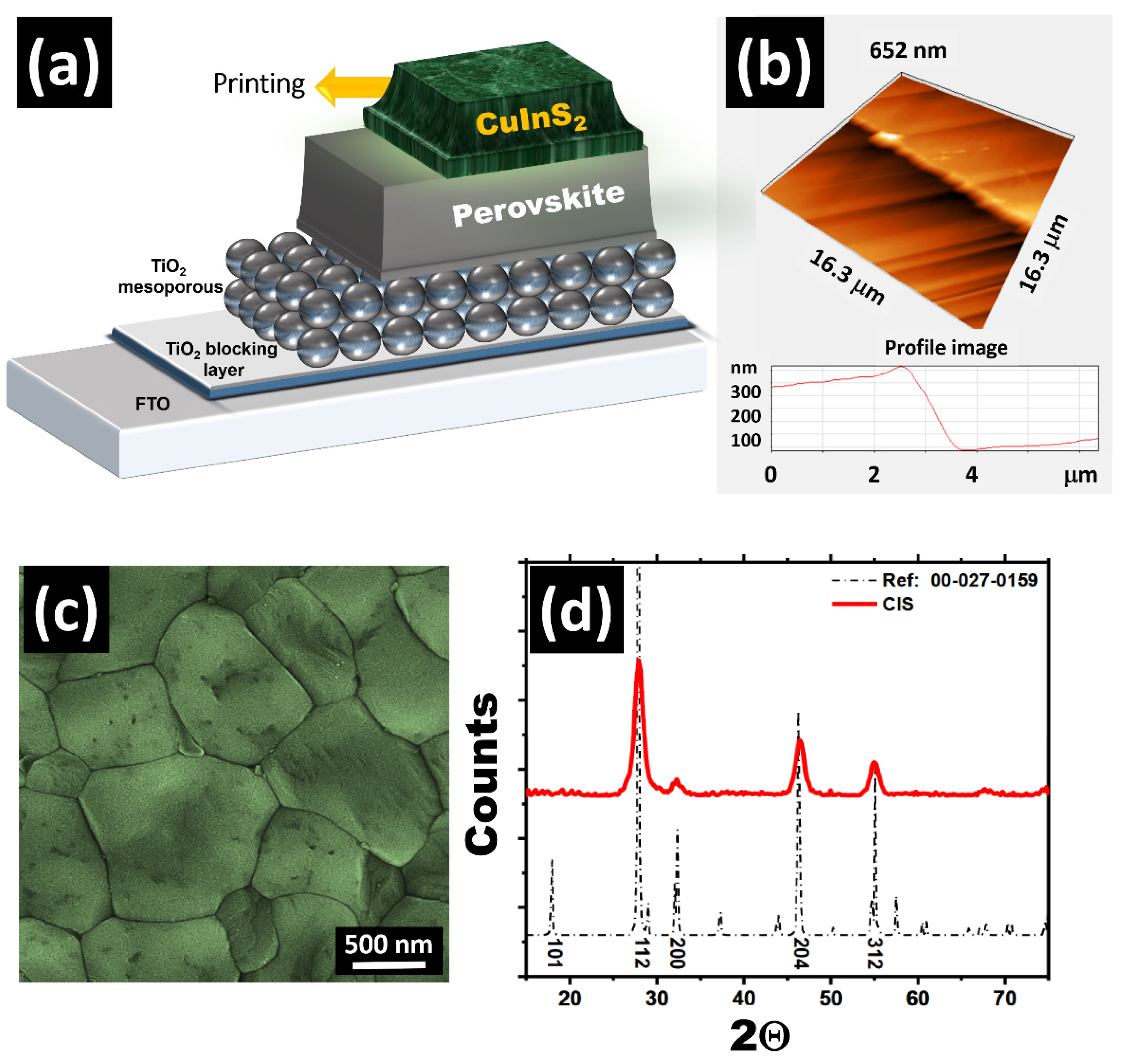
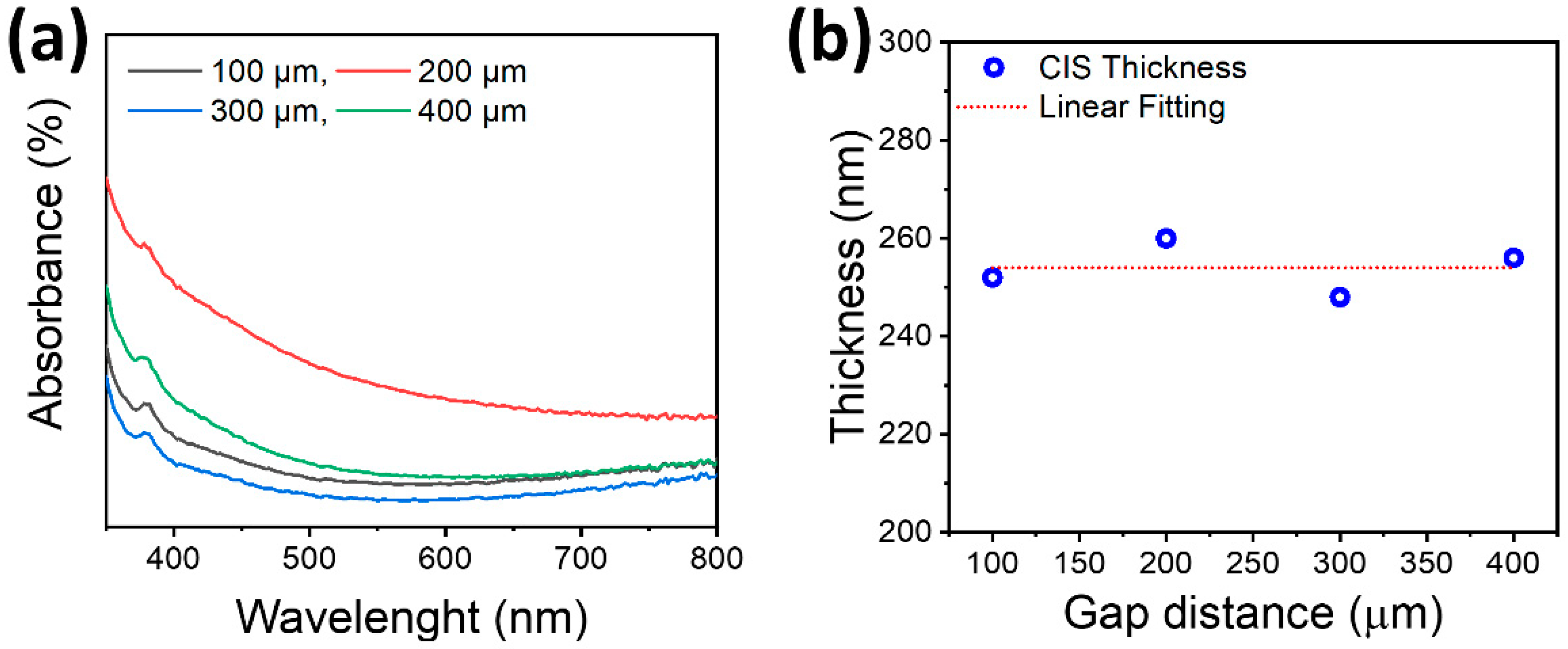
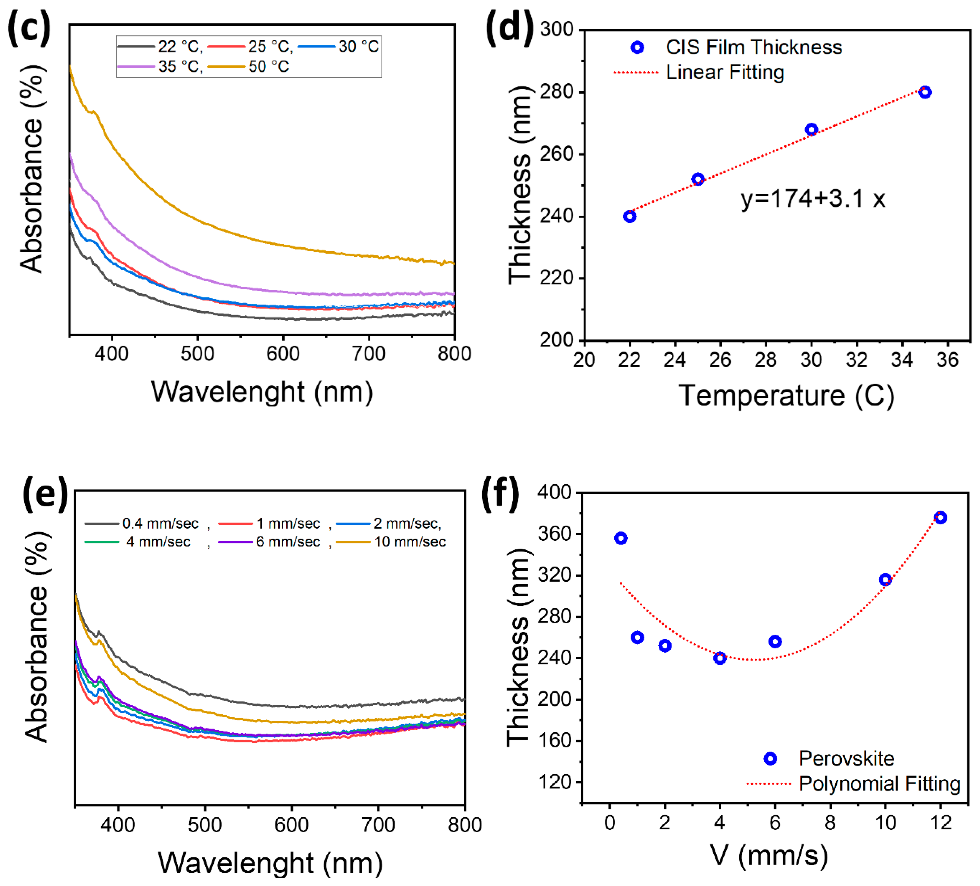
3.4. CuInS2 (CIS) as Hole Transport Layer

Figure 5a illustrates the printing schematics of CIS layer and its features. The thickness of around 250 nm was measured through AFM (Figure 5b). The top-view SEM image (Figure 5c) and the correspondence XRD illustrate the formation of CIS layer (Figure 5d). As it is evident, the crystalline CIS layer formed and the peaks are consistent with reference number 00-027-0159.
We investigated the effects of gap distance, bed temperature, and printing speed on layer thickness to determine the optimal printing conditions for the CIS layer. Maintaining homogeneity in the thickness of an inorganic ink presents numerous difficulties. To assess the effect of gap distance on layer thickness, we conducted printing at four distances: 100, 200, 300, and 400 μm. Figure 6a,b displays the results of printing at different gap distances, with thickness varying from 240 to 260 nm. Given the need for greater thickness in the CIS layer, its stability in the liquid bank, and its relative insensitivity to surface roughness, a 200-um gap was selected as the most suitable option. Absorbance data of printed films, as shown in Figure 6a, confirms the higher thickness of CIS films fabricated with the 200-um gap. The bed temperature is the second most critical parameter in printing. Figure 6c,d show the temperature analysis results by measuring absorbance and displaying related thickness. We examined different printing temperatures ranging from 22 to 36 °C. The optimal printing temperature of 25 °C was chosen due to the uniformity of the printed CIS film. Additionally, we avoided a higher thickness for the HTL to prevent an increase in series resistance in the complete device. In the final step, we utilized the printing speed to control the thickness of the layer, as shown in Figure 6e,f. This parameter has a direct impact on the layer thickness. While the thickness of the layer is a crucial parameter of interest for users of printing equipment, the quality control of the coating should also be given careful consideration. In general, a thin layer coated with slot-die coating should fall within the stable coating window range to ensure reliable and defect-free coating. Achieving a defect-free thin film of the desired thickness often requires balancing the ink injection speed and substrate movement speed. At low speeds, the drying time is comparable to the speed of movement, resulting in the solute collecting in the meniscus region and forming a solid film. At the other end of the spectrum is the Landau–Levich regime, where the coating rate is high enough to form wet layers that remain on the substrate during the printing timeframe due to relatively low drying. As the speed increases, the coating thickness decreases due to the reduced time available for the liquid to evaporate per unit length. If the coating speed is too fast, the liquid does not have enough time to evaporate in the meniscus and the coating operation enters the Landau–Levich regime. We finally settled on a printing speed of 12 mm/s for three steps. After each step, the printed film was transferred over the 100 °C hot plate. We encountered a problem with partial dissolving of the previously deposited layer. Due to instrument limitations, we were unable to test higher speeds without defects.

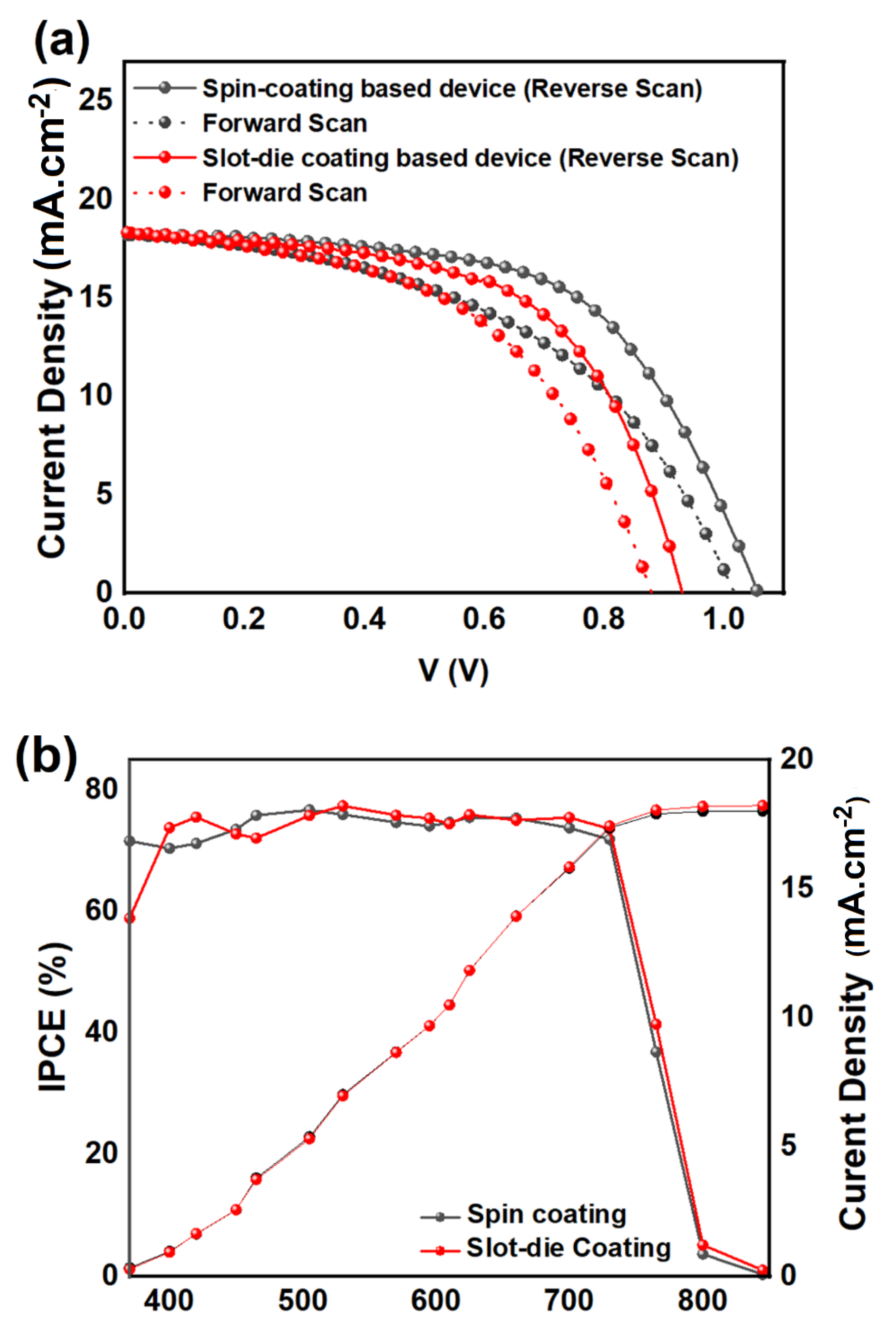
3.5. Photovoltaic Measurement

Figure 7a shows the solar cell performance fabricated through slot-die printing and spin-coating. The solar cell fabricated using the all-printing method exhibits a better short circuit current; however, this current declines rapidly during the voltage scan, indicating an increase in series resistance and a decrease in parallel resistance compared to the spin-coated solar cell (Table 3). It appears that the primary reason for the decline in cell efficiency in the all-print cell is the reduction in parallel resistance. Moreover, some of the series resistance in the printed cell is related to the printed carbon top electrode, which a modification can enhance to improve the cell’s efficiency. Additionally, the perovskite layer may have surface traps near its surface or within the bulk that can act as traps for electrons and holes. The printed cell efficiencies were comparable to the reference cell, with the best efficiency of 9.9% for a large-scale all-printed one compared to the 11.36% efficiency of spin-coated devices.
Using a narrow gap mold printing technique, we demonstrated the controllability of printed thin layer thicknesses on various substrates ranging from 3 × 3.5 cm2 to 3 × 10 cm2. We achieved a high printing rate of up to 1.2 cm/s and nearly 100% ink utilization. Using this deposition method in a free atmosphere without considering humidity, we obtained the highest efficiency of 9.9%. In contrast to the usual method of creating perovskite phase change using a vacuum, the substrate temperature needs to be between 35 and 45 °C to achieve suitable wetting for the substrate. However, in our case, we used ethyl acetate anti-solvent to form the phase and did not require increased substrate temperature. Figure 7b illustrates the IPCE results of both types of spin-coated and printed solar cells. Both cells exhibit similar behavior, with absorption predominantly related to the perovskite layer.

4. Conclusions

In conclusion, this research investigated the use of a fully printed perovskite solar cell with a hole transport layer made of CIS ink using an in-house assembled slot-die machine. The efficiency achieved was 9.9%, comparable to similar cells made using spin coating. It was determined that the CIS hole transport layer has suitable efficiency and other advantages, such as reduced cost, high processability, and easier synthesis, making it a good option for perovskite solar cell manufacturing. This research demonstrates the potential of using a printed CIS hole transport layer to produce perovskite solar cells. The method offers improved controllability of the thickness of the printed thin layers, which is critical for mass production, and less wastage of material, which is the aim of sustainability.

Supplementary Materials

The following supporting information can be downloaded at: https://www.mdpi.com/article/10.3390/su15086562/s1, Figure S1: fabricated slot-die coater head. (1—heating element housing; 2—front lip; 3—Back lip; 4—shim; 5—screw; 6—heating element stopper; 7—temperature sensor; 8—heating element; 9—alignment pins; 10–11—screw; 12—dispensing channel; 13–15 mounting accessories; 16—electromagnetic valve; 18—ink syringe pump connector). Figure S2: AFM profilometry of printed Block TiO2 film; Figure S3: transmittance spectra of the perovskite film at different printing speeds of (a) 1.5 mm/s, (b) 2 mm/s, (c) 3 mm/s, and (d) 4 mm/s; Figure S4: (a) absorbance spectra and (b) images of printed perovskite film at different substrate temperatures. An aluminum foil is placed under the layers for imaging with the camera; Figure S5: (a) PL spectra of printed perovskite films fabricated by anti-solvent and vacuum methods. (b) Camera image of vacuum-based and anti-solvent-based printed perovskite films; Figure S6: XRD data of printed perovskite film.

Author Contributions

Formal analysis, investigation, data curation, writing—original draft preparation, S.M. and M.H.; data curation, writing—original draft preparation, L.S., investigation, R.K.; data curation, writing—review and editing, supervision, R.M., project administration, funding acquisition, N.T. All authors have read and agreed to the published version of the manuscript.

Funding

This research received no external funding.

Institutional Review Board Statement

Not applicable.

Informed Consent Statement

Not applicable.

Data Availability Statement

All Data will be available on request.

Conflicts of Interest

The authors declare no conflict of interest.

References

  1. Basumatary, P.; Agarwal, P. A short review on progress in perovskite solar cells. Mater. Res. Bull. 2022, 149, 111700. [Google Scholar] [CrossRef]
  2. Cheng, Y.; Ding, L. Pushing commercialization of perovskite solar cells by improving their intrinsic stability. Energy Environ. Sci. 2021, 14, 3233–3255. [Google Scholar] [CrossRef]
  3. Lin, L.; Jones, T.W.; Yang, T.C.J.; Duffy, N.W.; Li, J.; Zhao, L.; Chi, B.; Wang, X.; Wilson, G.J. Inorganic electron transport materials in perovskite solar cells. Adv. Funct. Mater. 2021, 31, 2008300. [Google Scholar] [CrossRef]
  4. Zhang, H.; Ji, X.; Yao, H.; Fan, Q.; Yu, B.; Li, J. Review on efficiency improvement effort of perovskite solar cell. Sol. Energy 2022, 233, 421–434. [Google Scholar] [CrossRef]
  5. Chouhan, L.; Ghimire, S.; Subrahmanyam, C.; Miyasaka, T.; Biju, V. Synthesis, optoelectronic properties and applications of halide perovskites. Chem. Soc. Rev. 2020, 49, 2869–2885. [Google Scholar] [CrossRef] [PubMed]
  6. Coletta, V.C.; Gonçalves, R.V.; Bernardi, M.I.; Hanaor, D.A.; Assadi, M.H.N.; Marcos, F.C.; Nogueira, F.G.; Assaf, E.M.; Mastelaro, V.R. Cu-modified SrTiO3 perovskites toward enhanced water–gas shift catalysis: A combined experimental and computational study. ACS Appl. Energy Mater. 2020, 4, 452–461. [Google Scholar] [CrossRef]
  7. Dou, J.; Chen, Q. Interfacial Engineering for Improved Stability of Flexible Perovskite Solar Cells. Energy Mater. Adv. 2022, 2022, 0002. [Google Scholar] [CrossRef]
  8. Doustkhah, E.; Hassandoost, R.; Khataee, A.; Luque, R.; Assadi, M.H.N. Hard-templated metal–organic frameworks for advanced applications. Chem. Soc. Rev. 2021, 50, 2927–2953. [Google Scholar] [CrossRef]
  9. Li, M.; Huang, P.; Zhong, H. Current Understanding of Band-Edge Properties of Halide Perovskites: Urbach Tail, Rashba Splitting, and Exciton Binding Energy. J. Phys. Chem. Lett. 2023, 14, 1592–1603. [Google Scholar] [CrossRef]
  10. Shirsath, S.E.; Assadi, M.H.N.; Zhang, J.; Kumar, N.; Gaikwad, A.S.; Yang, J.; Maynard-Casely, H.E.; Tay, Y.Y.; Du, J.; Wang, H. Interface-Driven Multiferroicity in Cubic BaTiO3-SrTiO3 Nanocomposites. ACS Nano 2022, 16, 15413–15424. [Google Scholar] [CrossRef]
  11. Ye, M.; Biesold, G.M.; Zhang, M.; Wang, W.; Bai, T.; Lin, Z. Multifunctional quantum dot materials for perovskite solar cells: Charge transport, efficiency and stability. Nano Today 2021, 40, 101286. [Google Scholar] [CrossRef]
  12. Yang, X.; Li, Q.; Zheng, Y.; Luo, D.; Zhang, Y.; Tu, Y.; Zhao, L.; Wang, Y.; Xu, F.; Gong, Q. Perovskite hetero-bilayer for efficient charge-transport-layer-free solar cells. Joule 2022, 6, 1277–1289. [Google Scholar] [CrossRef]
  13. Sarkar, D.; Mottakin, M.; Hasan, A.M.; Selvanathan, V.; Sobayel, K.; Khan, M.; Rabbani, A.M.; Shahinuzzaman, M.; Aminuzzaman, M.; Anuar, F.H. A Comprehensive Study on RbGeI3 based Inorganic Perovskite Solar Cell using Green Synthesized CuCrO2 as Hole Conductor. J. Photochem. Photobiol. A Chem. 2023, 439, 114623. [Google Scholar] [CrossRef]
  14. Haider, S.Z.; Anwar, H.; Jamil, Y.; Shahid, M. A comparative study of interface engineering with different hole transport materials for high-performance perovskite solar cells. J. Phys. Chem. Solids 2020, 136, 109147. [Google Scholar] [CrossRef]
  15. Chen, L.; Qiu, L.; Wang, H.; Yuan, Y.; Song, L.; Xie, F.; Xiong, J.; Du, P. CuGaO2 Nanosheet Arrays as the Hole-Transport Layer in Inverted Perovskite Solar Cells. ACS Appl. Nano Mater. 2022, 5, 10055–10063. [Google Scholar] [CrossRef]
  16. Xu, H.; Lang, R.; Gao, C.; Yu, W.; Lu, W.; Mohammadi, S. Perovskite solar cells enhancement by CZTS based hole transport layer. Surf. Interfaces 2022, 33, 102187. [Google Scholar] [CrossRef]
  17. Ghavaminia, E.; Behrouznejad, F.; Forouzandeh, M.; Khosroshahi, R.; Darbari, S.; Zhan, Y.; Taghavinia, N. Polyvinylcarbazole as an Efficient Interfacial Modifier for Low-Cost Perovskite Solar Cells with CuInS2/Carbon Hole-Collecting Electrode. Solar RRL 2021, 5, 2100074. [Google Scholar] [CrossRef]
  18. Zhao, X.; Kim, H.-S.; Seo, J.-Y.; Park, N.-G. Effect of selective contacts on the thermal stability of perovskite solar cells. ACS Appl. Mater. Interfaces 2017, 9, 7148–7153. [Google Scholar] [CrossRef]
  19. Coughlan, C.; Ibanez, M.; Dobrozhan, O.; Singh, A.; Cabot, A.; Ryan, K.M. Compound copper chalcogenide nanocrystals. Chem. Rev. 2017, 117, 5865–6109. [Google Scholar] [CrossRef]
  20. Palchoudhury, S.; Ramasamy, K.; Gupta, A. Multinary copper-based chalcogenide nanocrystal systems from the perspective of device applications. Nanoscale Adv. 2020, 2, 3069–3082. [Google Scholar] [CrossRef]
  21. Valdés, M.; Berruet, M.; Goossens, A.; Vázquez, M. Spray deposition of CuInS2 on electrodeposited ZnO for low-cost solar cells. Surf. Coat. Technol. 2010, 204, 3995–4000. [Google Scholar] [CrossRef]
  22. Esmaeili-Zare, M.; Behpour, M. Influence of deposition parameters on surface morphology and application of CuInS2 thin films in solar cell and photocatalysis. Int. J. Hydrog. Energy 2020, 45, 16169–16182. [Google Scholar] [CrossRef]
  23. Lee, D.-Y.; Kim, J. Deposition of CuInS2 films by electrostatic field assisted ultrasonic spray pyrolysis. Sol. Energy Mater. Sol. Cells 2011, 95, 245–249. [Google Scholar] [CrossRef]
  24. Scheer, R.; Lewerenz, H.J. Formation of secondary phases in evaporated CuInS2 thin films: A surface analytical study. J. Vac. Sci. Technol. A: Vac. Surf. Film. 1995, 13, 1924–1929. [Google Scholar] [CrossRef]
  25. Tong, S.; Gong, C.; Zhang, C.; Liu, G.; Zhang, D.; Zhou, C.; Sun, J.; Xiao, S.; He, J.; Gao, Y. Fully-printed, flexible cesium-doped triple cation perovskite photodetector. Appl. Mater. Today 2019, 15, 389–397. [Google Scholar] [CrossRef]
  26. Wang, R.; Kwon, H.-J.; Tang, X.; Ye, H.; Park, C.E.; Kim, J.; Kong, H.; Kim, S.H. Slot-die coating of sol–gel-based organic–inorganic nanohybrid dielectric layers for flexible and large-area organic thin film transistors. Appl. Surf. Sci. 2020, 529, 147198. [Google Scholar] [CrossRef]
  27. Yadav, B.S.; Koppoju, S.; Dey, S.R.; Dhage, S.R. Microstructural investigation of inkjet printed Cu (In, Ga) Se2 thin film solar cell with improved efficiency. J. Alloy. Compd. 2020, 827, 154295. [Google Scholar] [CrossRef]
  28. De Kergommeaux, A.; Fiore, A.; Bruyant, N.; Chandezon, F.; Reiss, P.; Pron, A.; De Bettignies, R.; Faure-Vincent, J. Synthesis of colloidal CuInSe2 nanocrystals films for photovoltaic applications. Sol. Energy Mater. Sol. Cells 2011, 95, S39–S43. [Google Scholar] [CrossRef]
  29. Cai, L.; Liang, L.; Wu, J.; Ding, B.; Gao, L.; Fan, B. Large area perovskite solar cell module. J. Semicond. 2017, 38, 014006. [Google Scholar] [CrossRef]
  30. Zuo, C.; Vak, D.; Angmo, D.; Ding, L.; Gao, M. One-step roll-to-roll air processed high efficiency perovskite solar cells. Nano Energy 2018, 46, 185–192. [Google Scholar] [CrossRef]
  31. Gao, L.; Huang, K.; Long, C.; Zeng, F.; Liu, B.; Yang, J. Fully slot-die-coated perovskite solar cells in ambient condition. Appl. Phys. A 2020, 126, 452. [Google Scholar] [CrossRef]
  32. Di Giacomo, F.; Shanmugam, S.; Fledderus, H.; Bruijnaers, B.J.; Verhees, W.J.; Dorenkamper, M.S.; Veenstra, S.C.; Qiu, W.; Gehlhaar, R.; Merckx, T. Up-scalable sheet-to-sheet production of high efficiency perovskite module and solar cells on 6-in. substrate using slot die coating. Sol. Energy Mater. Sol. Cells 2018, 181, 53–59. [Google Scholar] [CrossRef]
  33. Yin, H.; Lv, P.; Gao, B.; Zhang, Y.; Zhu, Y.; Hu, M.; Tan, B.; Xu, M.; Huang, F.; Cheng, Y.-B. Slot-die coated scalable hole transporting layers for efficient perovskite solar modules. J. Mater. Chem. A 2022, 10, 25652–25660. [Google Scholar] [CrossRef]
  34. Lee, H.-J.; Seo, Y.-H.; Kim, S.-S.; Na, S.-I. Slot-die processed perovskite solar cells: Effects of solvent and temperature on device performances. Semicond. Sci. Technol. 2022, 37, 045007. [Google Scholar] [CrossRef]
  35. Yang, J.; Hu, Y.; Yan, B.; Chang, J.; Yao, J.; Han, H. Large-area Perovskite Optoelectronic Devices and the Fabrication Techniques. Perovskite Mater. Devices 2022, 2, 433–477. [Google Scholar]
  36. Qin, T.; Huang, W.; Kim, J.-E.; Vak, D.; Forsyth, C.; McNeill, C.R.; Cheng, Y.-B. Amorphous hole-transporting layer in slot-die coated perovskite solar cells. Nano Energy 2017, 31, 210–217. [Google Scholar] [CrossRef]
  37. Tutantsev, A.S.; Udalova, N.N.; Fateev, S.A.; Petrov, A.A.; Chengyuan, W.; Maksimov, E.G.; Goodilin, E.A.; Tarasov, A.B. New pigeonholing approach for selection of solvents relevant to lead halide perovskite processing. J. Phys. Chem. C 2020, 124, 11117–11123. [Google Scholar] [CrossRef]
  38. Barichello, J.; Di Girolamo, D.; Nonni, E.; Paci, B.; Generosi, A.; Kim, M.; Levtchenko, A.; Cacovich, S.; Di Carlo, A.; Matteocci, F. Semi-Transparent Blade-Coated FAPbBr3 Perovskite Solar Cells: A Scalable Low-Temperature Manufacturing Process under Ambient Condition. Sol. RRL 2023, 7, 2200739. [Google Scholar] [CrossRef]
  39. Mohammadi, M.; Gholipour, S.; Malekshahi Byranvand, M.; Abdi, Y.; Taghavinia, N.; Saliba, M. Encapsulation strategies for highly stable perovskite solar cells under severe stress testing: Damp heat, freezing, and outdoor illumination conditions. ACS Appl. Mater. Interfaces 2021, 13, 45455–45464. [Google Scholar] [CrossRef]
  40. Crowley, K.; Morrin, A.; Hernandez, A.; O’Malley, E.; Whitten, P.G.; Wallace, G.G.; Smyth, M.R.; Killard, A.J. Fabrication of an ammonia gas sensor using inkjet-printed polyaniline nanoparticles. Talanta 2008, 77, 710–717. [Google Scholar] [CrossRef]
Figure 1. In-house assembled slot-die machine equipped with slot-die head, micrometer, bed temperature controller, printing speed controller, syringe pump, and bed hotplate motorized X-Y table.
Sustainability 15 06562 g001
Figure 2. AFM images of TiO2 block layer deposited at (a) 20 °C and (b) 25 °C. (c) Changes in block layer thickness according to printing speed and number of layer depositions extracted from UV-vis data.
Sustainability 15 06562 g002aSustainability 15 06562 g002b
Figure 3. (a) Gap distance between the printing head and substrate vs. layered thickness and (b) printing speed vs. layered thickness of mp-TiO2 and perovskite thin films. There are two measures of thickness attitude vs. speed: evaporation and the Landau–Levich regime. (c) Dependence of thickness of mp-TiO2 layer on printing temperature. (d) Scanning electron microscopy image of mp-TiO2 utilizing slot-die printing method.
Sustainability 15 06562 g003
Figure 4. (a) Statistical data of printed perovskite film’s PL peak intensity at different substrate temperatures. (b) PL spectra of spin-coated and printed film. (c) Top-view FESEM image of printed perovskite film. (d) Perovskite film transverse thickness profile. The thicknesses were calculated from eight different points across the printed film thickness from absorbance data.
Sustainability 15 06562 g004
Figure 5. (a) Schematic of printing perovskite solar cells; (b) AFM profilometry; (c) Top-view SEM image; and (d) XRD of printed CIS film.
Sustainability 15 06562 g005
Figure 6. Relationship between absorbance (a,c,e) and thickness of CIS films (b,d,f) for various gap distances between the printing head and substrate (a,b), printing temperature (c,d), and printing speed (e,f). The film thickness as a function of deposition speed has two behaviors known as evaporation and the Landau–Levich regime. In the references, the slope of these two behaviors is identified. In this experiment, as we are working in a small area some deviations are seen that could be more seen in the evaporation part. The change of behavior in film thickness could be seen obviously.
Sustainability 15 06562 g006aSustainability 15 06562 g006b
Figure 7. Photovoltaic characterization (a) Current density–voltage measurement and (b) IPCE of spin-coated and slot-die coated perovskite solar cell.
Sustainability 15 06562 g007
Table 1. Blocking layer TiO2 printing parameters.
CriteriaBest ValueDescription
Reservoir temperature20 °C-
Head temperature20 °C-
Substrate temperature20 °CTemperature regulated
Printing speed3 mm/sFour step
Printing head typeroller printer30 mm diameter
Slot-die shim 15 µmStainless steel
Printing gap200 µm-
Post printing process Thermal annealing at 500 °C for 1 h
Substrate preparationUV-ozone 15 min
Table 2. Perovskite ink printing parameters.
CriteriaBest ValueDescription
Reservoir temperature25 ± 5 °C-
Head temperature25 ± 5 °C-
Substrate temperature40 ± 5 °CIn the case of anti-solvent use, we prefer to stay at room temperature, while using 20–25 °C for substrate temperature
Printing speed2 cm/sOne step
Printing head typeroller printer30 mm diameter
Slot-die shim 15 µmStainless steel
Printing gap200 µm-
Post printing process -
Substrate preparationUV-ozone 15 min
Table 3. Photovoltaic properties of devices.
SampleVoc (V)Jsc (mA·cm−2)FFEfficiency (%)Average (%)Hysteresis Index
Spin coating (reverse scan)1.05618.200.5911.369.36 ± 1430.22
Forward scan1.0218.200.488.91
Slot-die coating (reverse scan)0.9318.330.589.937.74 ± 1.440.17
Forward scan0.8818.330.518.23
Disclaimer/Publisher’s Note: The statements, opinions and data contained in all publications are solely those of the individual author(s) and contributor(s) and not of MDPI and/or the editor(s). MDPI and/or the editor(s) disclaim responsibility for any injury to people or property resulting from any ideas, methods, instructions or products referred to in the content.

