Abstract
Energy harvesting from cleaner sources and preserving the environment from dangerous gasses are presently the key priorities globally to maintain sustainable development. In this context, photovoltaic technology plays a vital role in generating energy from ternary organic solar cells. Ternary organic solar cells display significant potential for achieving outstanding photovoltaic performance compared to binary structures. Over the past few years, significant endeavors to develop novel organic materials have led to a consistent rise in efficiency, surpassing 19% for single-junction devices. In our study, we simulated an inverted ternary organic solar cell (TOSC) structure employing the one-dimensional optical and drift diffusion model and using “Oghma-Nano 8.0.034” software by optimizing the active blend thickness at 80 nm within the structure of ITO/SnO2/PM6:D18:L8-BO/PEDOT:PSS/Ag. We simulated different performance parameters such as EQE, Photo-CELIV, PCE, Jsc, Voc, and FF with different active layer thicknesses ranging from 50 to 200 nm to discover the behavior of the device in terms of efficiency parameters. Furthermore, the structure attained a PCE of 20% for an active layer thickness of 80 nm within a Jsc of 27.2 mA cm−2, a Voc of 0.89 V, and an FF of 82.3%. This approach can potentially be valuable in constructing a highly effective TOSC model in the laboratory.
1. Introduction
Photovoltaic (PV) technology is crucial in our shift towards cleaner and more sustainable energy sources. This technology minimizes greenhouse gas emissions and contributes to attaining the sustainable development goals. By harvesting solar energy, PV systems help isolate economic operations from environmental effects, encouraging a more sustainable future.
Organic solar cells (OSCs) have garnered considerable attention from the literature because of their reduced production cost, high flexibility, and low-temperature processing [1,2,3,4,5,6,7,8,9,10]. Furthermore, this technology needs to be improved in terms of efficiency. To optimize efficiency and facilitate the process of commercialization, it is essential to focus on improving key factors such as open-circuit voltage (Voc), short-circuit current (Jsc), and fill factor (FF). These parameters are directly affected by several factors, such as absorption of light, exciton generation, diffusion, dissociation, and transport. The adoption of innovative materials and the strategic configuration of electron donor–electron acceptor (D–A) pairs have emerged as crucial factors in attaining our objectives and improving the PCE. Ternary bulk heterojunction (BHJ) structures hold significance due to their potential to improve the efficiency of OSCs [11]. Integrating the ternary active layer has resulted in enhanced efficient charge transport and collection by the electrodes [12,13,14]. The absorption wavelength of the non-fullerene acceptors (NFAs) and the donor exhibit a complimentary absorption, leading to an augmentation in light absorption of the ternary active blend [15]. Recent advancements have shown how effective the ternary method is for OSCs. The attainment of such enthusiasm is accomplished through the collaborative enhancement of both charge mobility and transport. The third component added to the active layer is an intermediary unit that improves the efficiency of charge transport, increases the exciton lifetime, and provides a low recombination prefactor [16,17,18,19,20].
Organic hybrid materials nanoscale (OghmaNano) is a specialized software application specifically created to simulate the behavior of organic and hybrid solar cells. The modelling of disordered materials is characterized by its exact approach, which uses a non-equilibrium model to depict trapped carriers [21]. This enables realistic simulations of disordered materials across several domains, including steady-state, temporal, and frequency domains. Furthermore, the Shockley–Read–Hall formalism is employed to simulate charge transport in organic materials accurately. This software offers electrical and optical models, which solve equations about electron and hole transport, carrier continuity, drift diffusion, and estimation of electrostatic potential [21]. OghmaNano is highly advantageous for modeling ternary organic solar cells (TOSCs) by incorporating an extra substance [22]. The primary objective of TOSCs is to enhance efficiency. Furthermore, OghmaNano is a powerful tool for researchers and engineers involved in the design of organic and hybrid solar cells. It can simulate a range of optoelectronic devices such as solar cells, OLEDs, diodes, and FETs. This software offers exact modeling capabilities and assists in optimizing the performance of these devices [21,22]. The thickness and materials utilized for the interface layers also have a vital effect on cell performance. This is due to the ohmic contact of a low work function metal oxide with an electron acceptor that creates low series resistance (Rs), selectively transfers electrons, and enhances parallel resistance (Rsh) [23]. Therefore, the optimization of the active layer thickness is a vital part of solar cell design and modeling. It directly affects the efficiency, cost, and overall performance of the solar cell [24]. The charge transport layer is an important component of OSCs due to its key function in facilitating the extraction of charges from the active blend [25,26,27]. The facilitation of charge extraction contributes to the enhancement of PCE [28,29,30,31,32,33]. PEDOT:PSS has been a prominent choice for the hole transport layer (HTL) because of its notable electrical conductivity [34]. PEDOT:PSS is widely used by the most efficient OSC structures, and, importantly, represents the most efficient structure to date [35]. The application of tin dioxide (SnO2) as the electron transport layer (ETL) in OSCs has drawn significant interest owing to their outstanding electrical characteristics and remarkable stability [36,37]. Di Mario et al. introduced an inverted structure known as the n-i-p configuration, shown by utilizing SnO2 as the ETL. The PM6:L8-BO OSCs exhibited a notable PCE of 17.26% and an FF of 79% while employing atomic layer deposition (ALD)-SnO2 as the ETL [38].
The third component in TOSCs plays a significant role in boosting the overall efficiency of the device by enhancing photon harvesting [39]. This leads to better photon harvesting in the near-infrared region. In addition, the third component affects the nanomorphology of the bulk heterojunction within the active layer. Properly tailored morphology promotes charge separation and transport, decreasing recombination losses [39].
Several research has achieved record efficiency exceeding 19% for single-junction solar cells utilizing ternary blends [40,41,42]. Understanding how the third component influences charge and energy transmission is critical. It can accelerate exciton dissociation and charge extraction [42].
TOSCs have also shown potential in alleviating stability difficulties compared to binary solar cells. In summary, the third component in TOSCs plays a crucial role in obtaining high efficiency, enhancing photon harvesting, and optimizing active layer shape [41].
In this paper, we simulated a customized structure of ternary OSCs of ITO/SnO2/PM6:D18:L8-BO (a blend of organic materials)/PEDOT:PSS/Ag using the one-dimensional optical and drift diffusion model and using OghmaNano software, which has achieved a high PCE of 20%. The achievement of high efficiency in this work can be useful in fabricating an efficient TOSC model in the laboratory.
2. Simulation Models and Performance Indicators
The simulation uses “Oghma-Nano 8.0.034” software that is designed to address and solve the electrical and optical equations to get the performance results including PCE, Voc, Jsc, and FF. The electric model includes Poisson’s equation, free charge carrier statistics, and drift diffusion equations of charge carriers, while the optical model includes the Maxwell equations in the frequency domain. The structure of the simulated device is ITO/SnO2/PM6:D18:L8-BO/PEDOT:PSS/Ag based on the solution of the following two models, and the details of the input optical and electrical parameters are mentioned in Table 1 and Table 2 and Figure 1 and Figure 2, and the details of the software in these references [43,44,45].

Table 1.
The thickness of the materials used for OSCs for optimum efficiency.
Table 2.
Simulation parameters of OghmaNano software.

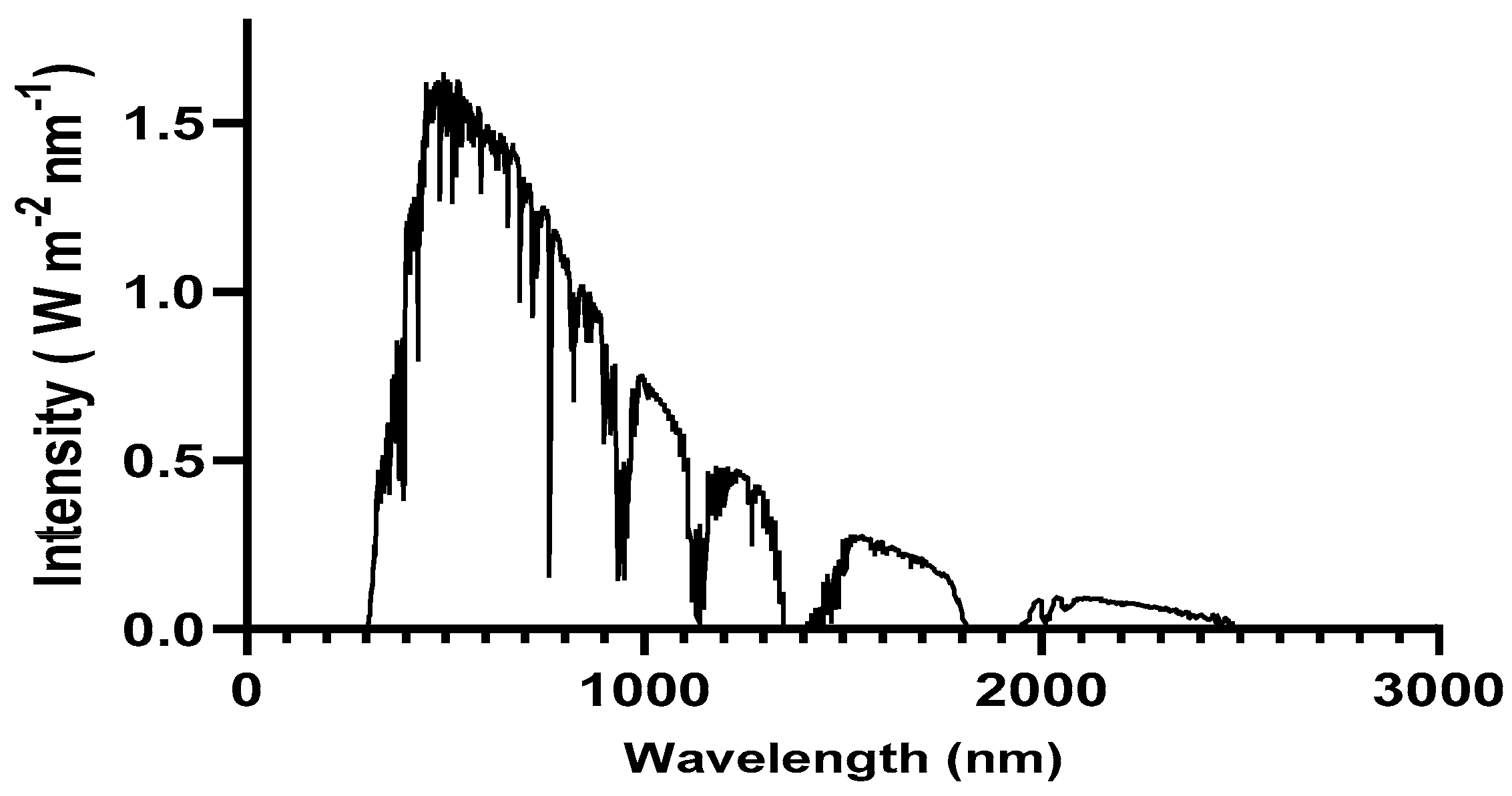
Figure 1.
Solar spectrum irradiance at AM 1.5 G.

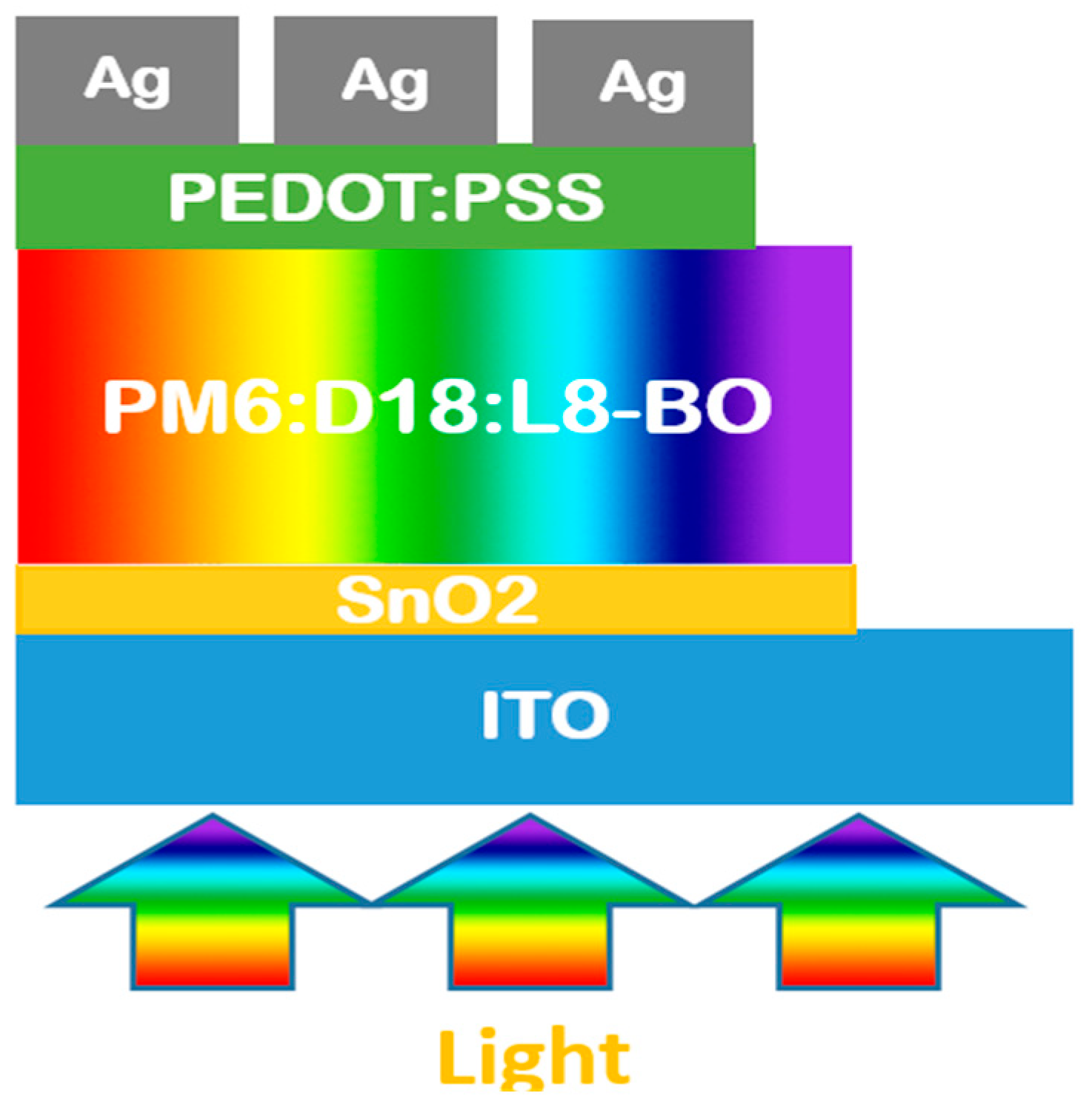
Figure 2.
The one-dimensional structure of our inverted ternary organic solar cell model under light exposure.
2.1. Optical Model
Maxwell’s equation for the frequency domain is used in the optical model in one dimension to calculate the distribution of photons as mentioned in Equations (1) and (2),
And
where E1,2 represent the electric field on the layers before and after the interface and k1,2 is the wave vector of the plane wave on the layers before and after the interface. The relationship between a plane wave’s electric and magnetic fields can expressed as follows:
where H is the magnetic field in the layers before and after the interface, ω is the frequency, and µ is the permeability of the medium through which the wave is propagating. Equation (3) can be applied to Equations (1) and (2), as shown in Equations (4) and (5):
Thus, the following equations are obtained:
Eventually, Equations (6) and (7) depicted the propagation of an electromagnetic field for a plane wave.
To solve the above model, we apply the electric and magnetic boundary conditions as follows:
where is the unit surface normal, at x = 0, which depicts the following:
The wave vector is given by Equation (12) as follows:
where ᶇ is the refractive index, λ is the wavelength, and c is the speed of light. Eventually, the electromagnetic boundary condition is depicted in Equation (13) as follows:
where η1,2 is the surface normal of the layers before and after the interface.
2.2. Electric Model
The solution to Poisson’s equation is used to determine the potential distribution within the semiconductor OSC, and it is represented as follows in Equation (14):
where ε0 and εr represent the constants of free space and the relative permittivity, respectively; φ is the electric field; q is the charge; n is the density of electrons; and p is the density of holes.
To solve free charge carriers in our study, the model applies Maxwell–Boltzmann statistics as mentioned in Equations (15) and (16), which represent the solution of the equations of carrier densities of electrons and holes as follows:
where Nc and Nv are the constants of the effective density of states in the conduction and valence band of a semiconductor, respectively; Fn,p is the fermi level in the valence and conduction band of a semiconductor; Ec is the conduction band; Ev is the valence band; T is the temperature; and KB is Boltzmann constant.
The transport of charge carriers is described by solving the drift diffusion equations within the position for both electrons and holes as mentioned in Equations (17) and (18) below:
where Jn,p is the current density of holes and electrons; µe,h are the electron and hole mobilities, respectively; and Dn,p are the electron and hole diffusion coefficient, respectively. Resolving the carrier continuity equations ensures charge carrier conservation as mentioned in Equations (19) and (20):
where Rn and p are the recombination of electrons and holes, respectively; G is the generation rate.
To solve the above electric model, we use the tunneling of electrons and holes through layer interfaces as the boundary conditions as follows:
where Te and Th is the rate constants of tunneling of electrons and holes, respectively; n1,2 is the number of electrons in the layers before and after the interface; p1,2 is the number of holes before and after the interface; is the equilibrium number of electrons in before and after the interface; and is the equilibrium number of holes in the layers before and after the interface. For more information on the optical and electrical models above, one can refer to these references [39,40,41].
2.3. Evaluation of Performance Indicators
The goal of our study is enhancing the PCE of OSCs, which is represented by Equation (23) as follows:
where Pmax is the maximum power released by the solar cell, and Iin is the illumination intensity. Voc value represents the highest voltage when there is null through the device, and it is represented as follows in Equation (24):
where Eg is the bandgap energy; Ef,h is the quasi-Fermi level of the holes in the valence band; and Ef,e is the quasi-Fermi level of the electrons in the conduction band.
Using and as included in Table 3, the following equations are obtained:
where is the energy offset. The FF defines the maximum power output of the OSC, it is defined below in Equation (27):
where A is the ideality factor of the semiconductor.
Table 3.
The PCE parameter output of our device from the variations of the active layer thickness.
3. Results and Discussion
3.1. Device Performance
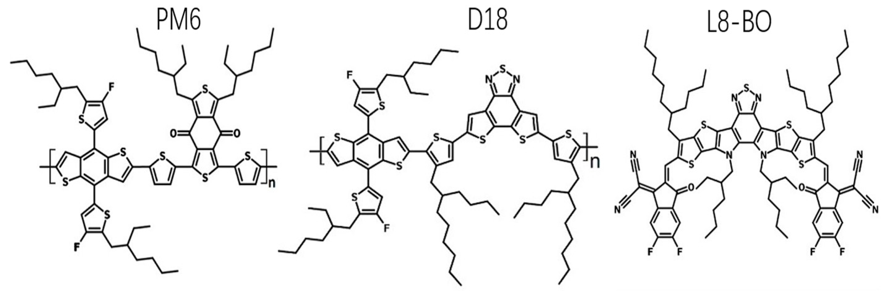
Figure 3 displays the chemical architectures and wavelength of the materials employed. L8-BO predominantly absorbs photons from 550 to 900 nm [46]. PM6 and D18 serve as a means to capture photons with short wavelengths ranging from 400 to 700 nm [46]. Additionally, this combination facilitates the manipulation of material crystallization processes, resulting in the formation of a donor phase characterized by high-quality crystalline properties.

Figure 3.
Chemical architectures of PM6, D18, and L8-BO.
The density of J-V characteristics was simulated under AM 1.5 G (see Figure 1) illumination with an intensity of 100 mW cm−2. These results are presented in Figure 4c and Table 3. Our device composed of the PM6:D18:L8-BO architecture demonstrates a PCE of 19.95%. Additionally, it delivers a Voc of 0.89 V, Jsc of 27.2 mA cm−2, and FF of 82.3%.
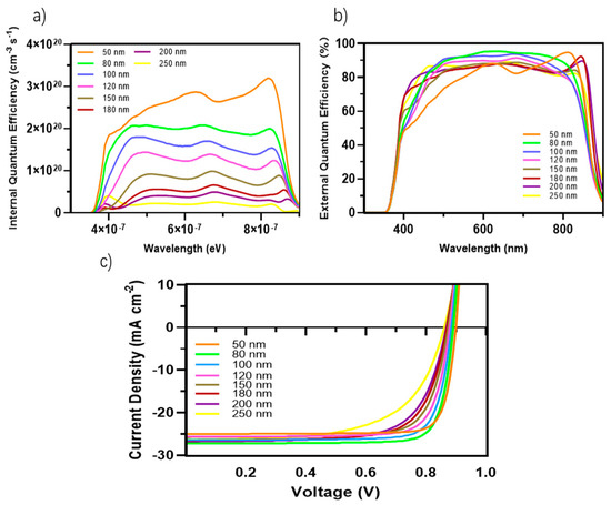
Figure 4.
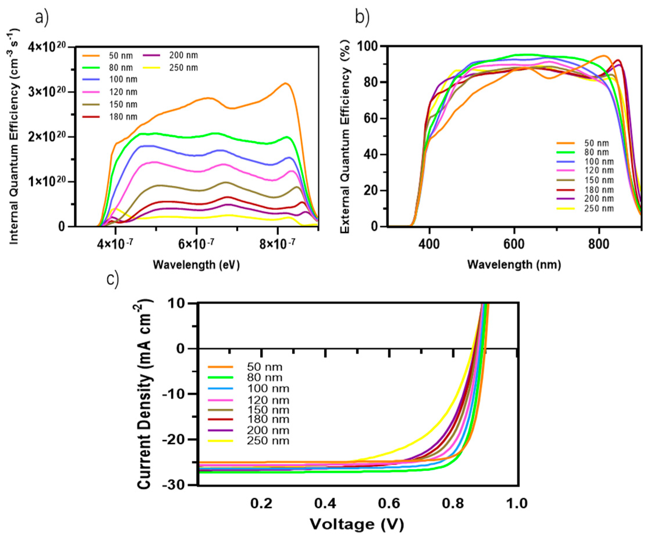
(a) Internal quantum efficiency (IQE) of the OSCs with different active layer thicknesses; (b) External quantum efficiency (EQE) of the devices with different active layer thicknesses; (c) J-V curves of the devices based on PM6:D18:L8-BO with a device area of 4.84 mm2 and different active layer thicknesses.
Light absorption and exciton generation were generally improved with increasing active layer thickness. However, this augmentation also results in an extended travel distance for charge carriers to reach the electrodes, then potentially causing higher recombination and diminished Jsc. If we apply this basic principle to our PCE parameters results within the variation of the active layer thicknesses, we notice from Table 3 that Voc and FF are relatively diminished when we increased the thickness of the active blend from 50 nm to 250 nm with a Voc decrease from 0.899 V to 0.86 V, respectively, and FF decrease from 84% to 61.8%, respectively. The Jsc increased from 25 mA cm−2 for 50 nm thickness to 27.2 mA cm−2 for 80 nm thickness and then decreased slightly through the different thicknesses until it reached a value of 26.3 mA cm−2 at 250 nm thickness.
The decrease in Voc and FF can be attributed to several factors. First, the extended travel distance that charge carriers must traverse to reach the interfaces plays a role. Additionally, an increase in the energy offset (ΔE) further aggravates this effect. Furthermore, the organic semiconductors used in these systems have a short exciton diffusion length, which leads to increased recombination losses.
The diffusion of excitons within the organic active layer is constrained due to the limited exciton diffusion length. Hence, it is imperative to establish an optimal balance between the broad absorption wavelength to maximize exciton generation and minimize the distance traveled by charge carriers to reach the electrodes. The Jsc exhibited a slight decrease as the thickness of the material increased, with values ranging from 25 mAcm−2 for a thickness of 50 nm to 27.2 mA cm−2 for a thickness of 80 nm. Nevertheless, when the thickness was 250 nm, the Jsc value was 26.3 mA cm−2. The observed increase in the Jsc of 27.2 mA cm−2 can be attributable to the ideal ratio attained at a thickness of 80 nm. At this thickness (80 nm), the absorption broadening and the diffusion of electron–hole pairs are successfully balanced. The specified thickness can be regarded as the optimal operating point for our device. Moreover, with this thickness, we achieved a Voc value of 0.89 V and an FF value of 82.3 %. The increased FF value for TOSCs is attributed to the optimization of the solar cell’s active layer, which necessitates a bicontinuous structure with well-formed and consolidated nanoscale domains. This relies on efficient charge transport and minimized recombination.
Furthermore, the inclusion of a third component can expand the absorption spectrum, resulting in a broader range of wavelengths that can be absorbed. This leads to improved light harvesting capabilities and an increase in the short-circuit current [47]. In addition, the third component can help to inhibit the morphological changes of the host mixture, leading to improved stability [48]. It also acts as a connecting unit to systematically enhance the charge movement, exciton lifespan, recombination, and nanomorphology [49].
3.2. Charge Carrier Generation, Transport, and Recombination
The EQE and IQE for the active blend made up of PM6:D18:L8-BO are shown in Figure 4a,b. The results indicate a broad absorption wavelength from 370 nm to 890 nm, as depicted in Figure 5 and Figure 6. This extensive absorption range contributes significantly to the generation rate of excitons, as evidenced in Figure 6. Moreover, the donors in this material combination possess superior crystallinity properties, which facilitate the diffusion and dissociation of excitons. Consequently, the Jsc increased.
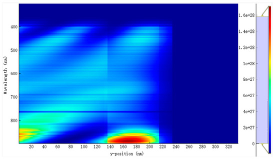
Figure 5.
The distribution of the spectrum of incident photons of the D–A active layer PM6:D18:L8-BO.

Figure 6.
The distribution of the spectrum of the absorbed photons of the D–A active layer PM6:D18:L8-BO.
Several factors must be taken into consideration while optimizing the active thickness, including the light-scattering properties of the material, the mobility of charge, the absorption coefficient, and the length of excitons diffusion. Consequently, there is a delicate equilibrium between maximizing photon absorption and minimizing charge recombination in the process of establishing the ideal thickness for the active layer. In our study of the EQE and IQE, we observed a decrease in the absorption rate for EQE when the active blend thickness was reduced to 50 nm. This decrease can be attributed to the narrow absorption wavelength associated with this thickness. However, we also observed a significant exciton generation rate for IQE due to the favorable exciton diffusion length. Specifically, the top generation rates were found to be 2.9 × 1020 cm−3 s−1 and 3.2 × 1020 cm−3 s−1 at energy levels of 6.22 × 10⁻⁷ eV and 8.12 × 10⁻⁷ eV, respectively.
The lowered thickness of the active blend results in a shorter travel distance for charge carriers to reach the charge transport layers and, subsequently, the electrodes. In our investigation, it was observed that a film with a thickness of 250 nm exhibits a broad absorption spectrum but a relatively low generation rate. Specifically, the highest generation rates were found to be 4.9 × 1020 cm−3 s−1 and 4.4 × 1020 cm−3 s−1 at energy levels of 3.92 × 10⁻⁷ eV and 8.32 × 10⁻⁷ eV, respectively. By doing a comparative analysis of the two thicknesses, we can validate the previously identified factors influencing the selection of the active layer thickness. Additionally, this analysis allows us to establish the ideal ratio between light absorption and minimizing charge recombination, taking into consideration the excitons diffusion length. Based on our research settings, which included considerations such as the crystallinity of the chosen materials, compatibility of the material’s absorption wavelength, and the alignment of the different materials energy levels, we determined that an ideal size of the active blend is 80 nm according to our performance results. This size range corresponded to an absorption wavelength between 370 nm and 890 nm.
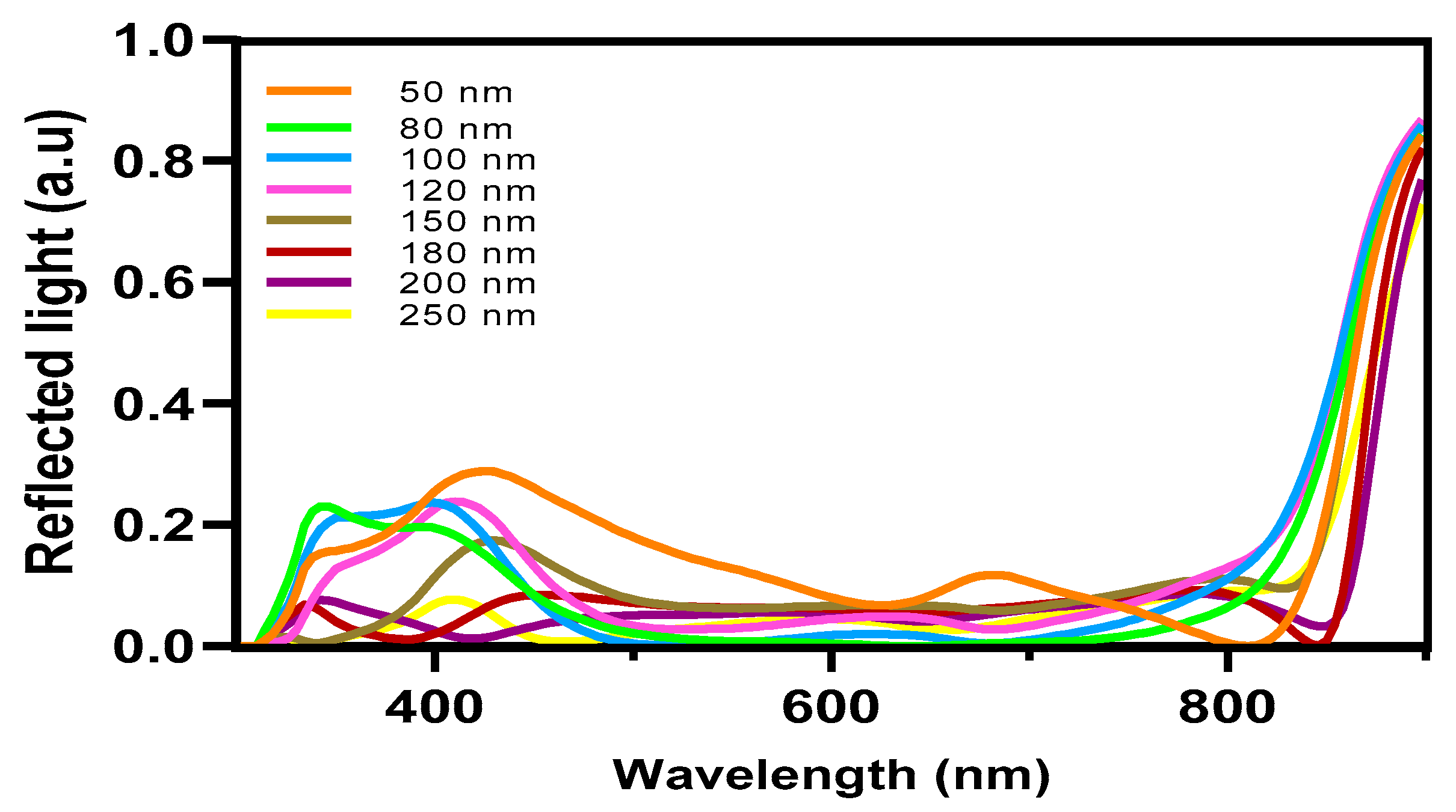
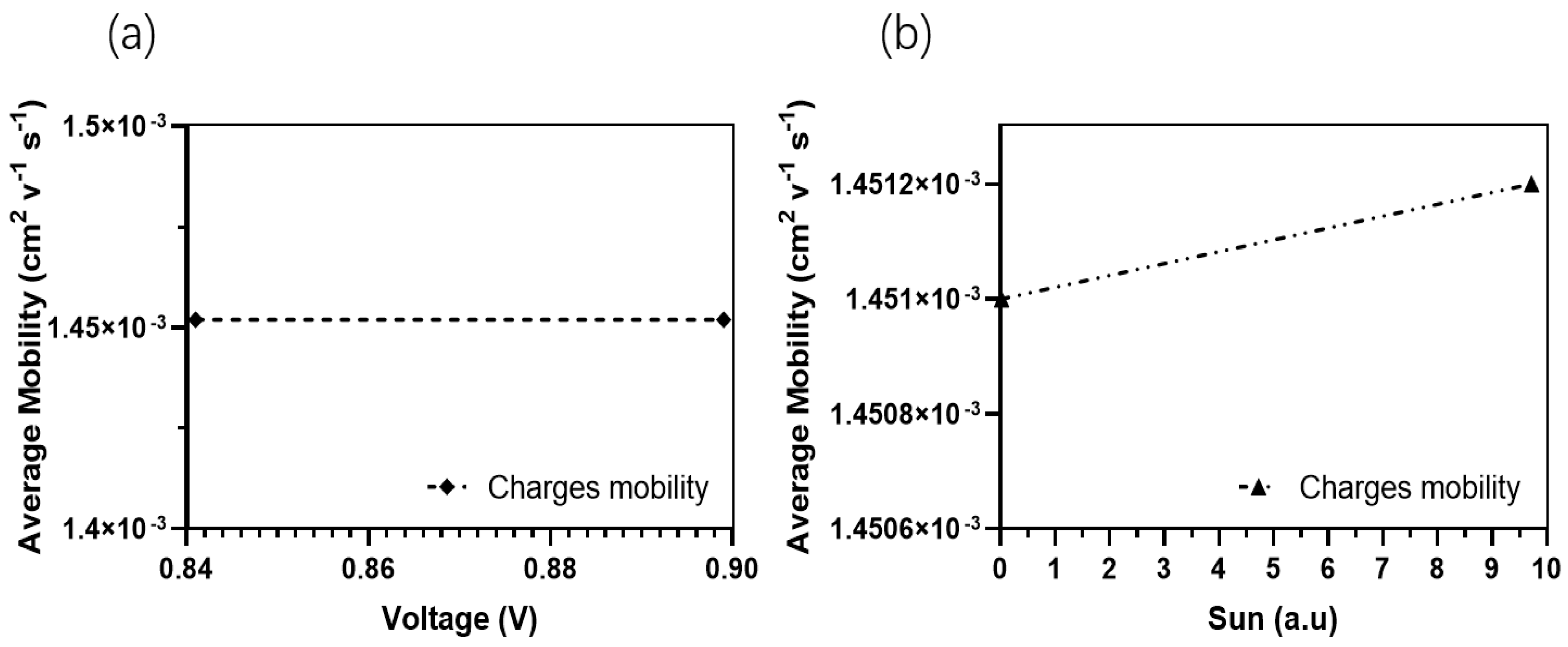
In contrast, the average absorption of photons within this wavelength range for other thicknesses ranges around 80%, with generation rates varying from 2.8 × 1020 cm−3 s−1 (50 nm) to a lower generation rate of 2.5 × 1020 cm−3 s−1. The confirmed values of the light’s absorption efficiency can be observed in Figure 7, which depicts the reflected light across various wavelengths. The diminished efficiency observed in the current generation of thick devices can be caused by the limited exciton diffusion length. Despite their strong light absorption capabilities, these materials have challenges in effectively separating electrons and holes due to diffusion limitations. The mobility of charge carriers is a critical factor in influencing the operational efficiency of OSCs. Figure 8a,b illustrates the fluctuation of this significant parameter as a function of the intensity of light and voltage for thicknesses spanning from 50 nm to 250 nm. In Figure 8b, it can be observed that there is a slight rise in charge carrier mobility as the light intensity is increased for all thicknesses. Notably, the average value is 1.4517 × 10⁻⁴ cm2 V−1 s−1.

Figure 7.
The reflected light of OSCs.
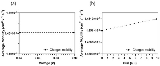
Figure 8.
Charges carrier mobilities for the optimal device. (a) Charges carrier mobility in the function of suns (a.u.); (b) Charges carrier mobility in the function of Voc.
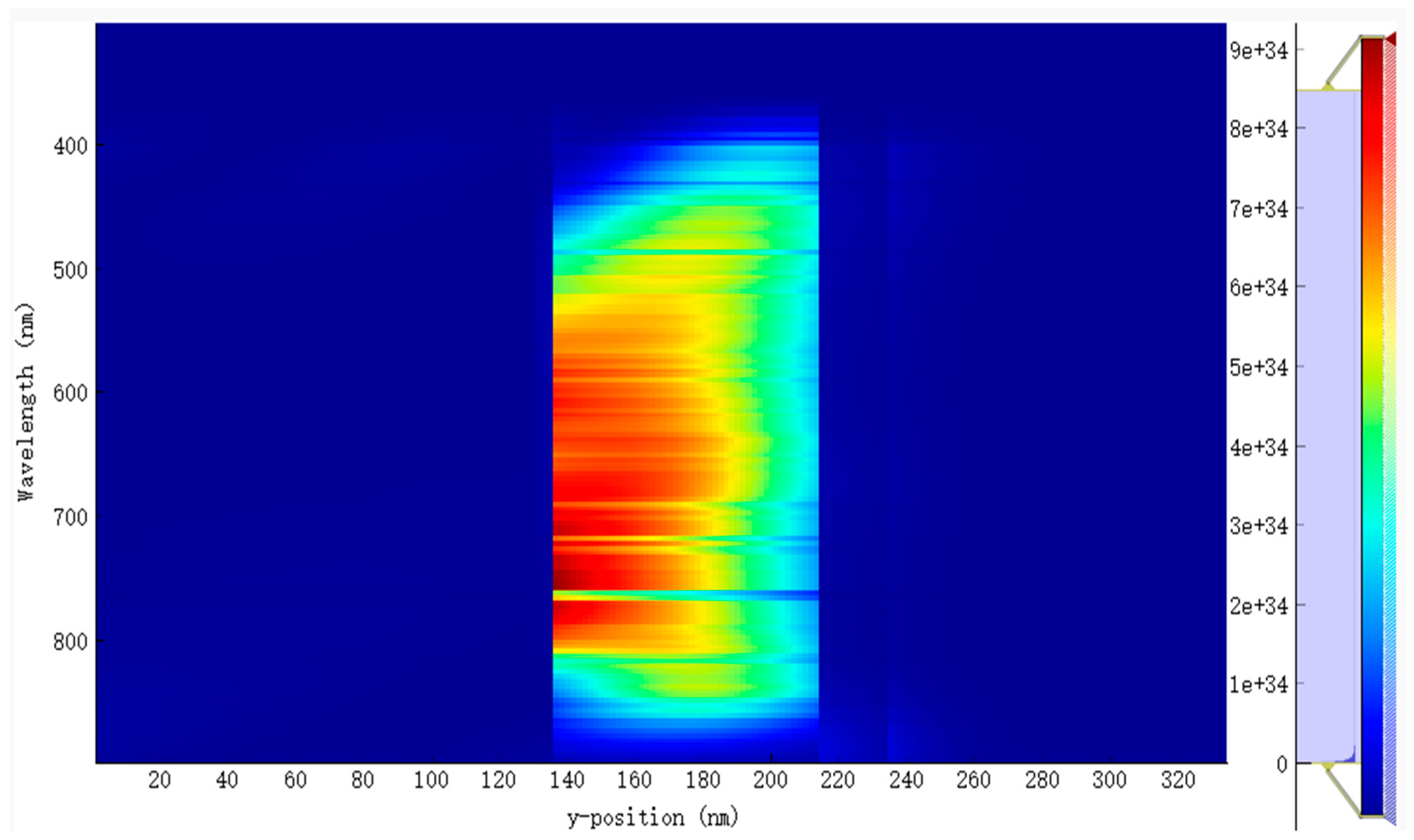
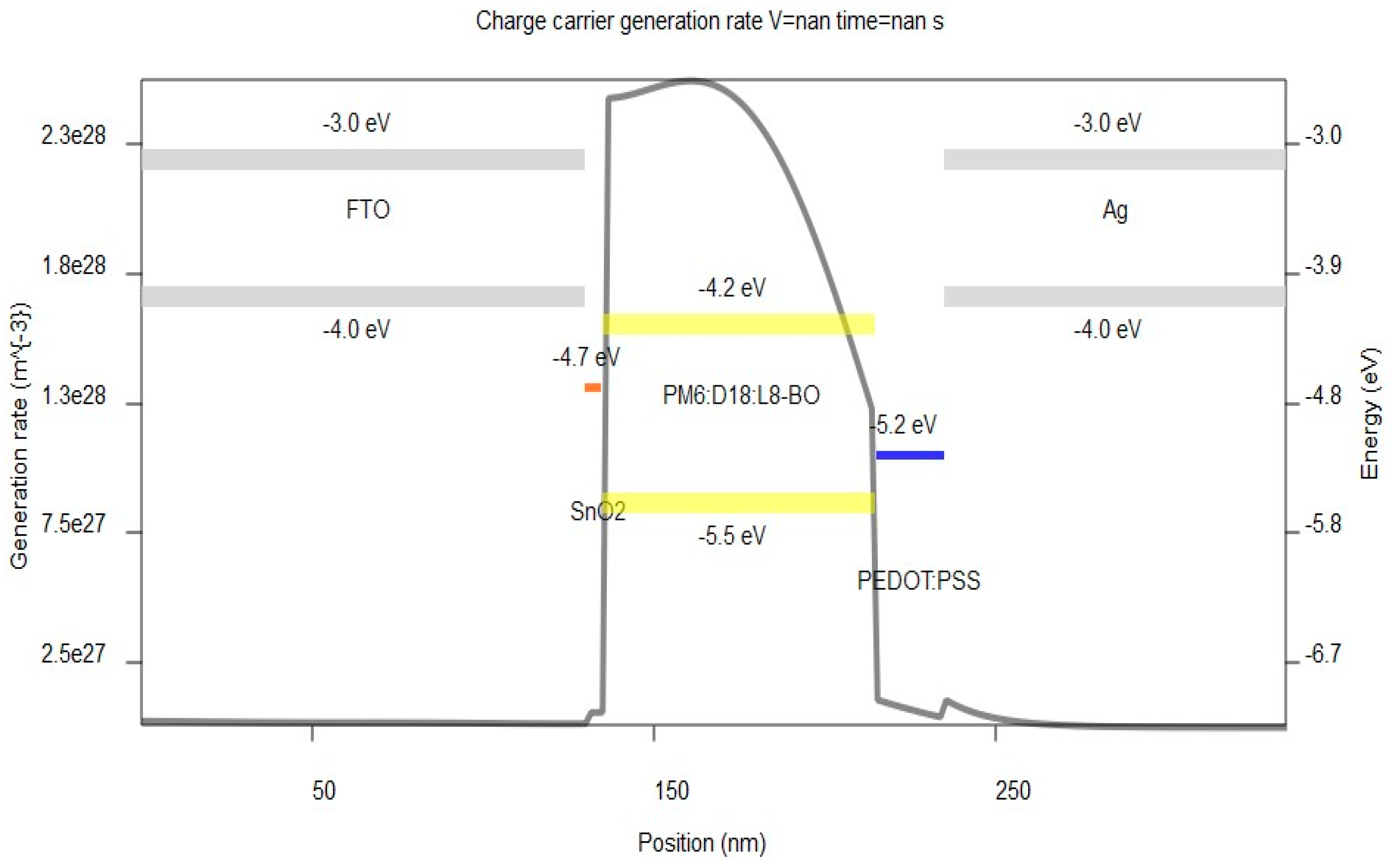
In Figure 9, it is observed that the active layer exhibits the highest occupied molecular orbital (HOMO) energy of −5.50 eV and the lowest unoccupied molecular orbital (LUMO) energy of −4.20 eV. Notably, there exists a significant cascaded pathway through the HOMO of the active blend and the PEDOT:PSS that has a HOMO of −5.20 eV, which effectively accelerates the transport of holes towards the electrode, while SnO2 has a LUMO of −4.70 eV, therefore enhancing the Voc. Equation (28) depicting the ΔE is a pivotal quantity that exerts a substantial influence on the efficiency of charge transport. If the change in ΔE exceeds or equals the value of the exciton binding energy (EB), it is plausible that the vibrational energy of the liberated molecule might potentially induce the separation of excitons into freely mobile electrons and holes [50].
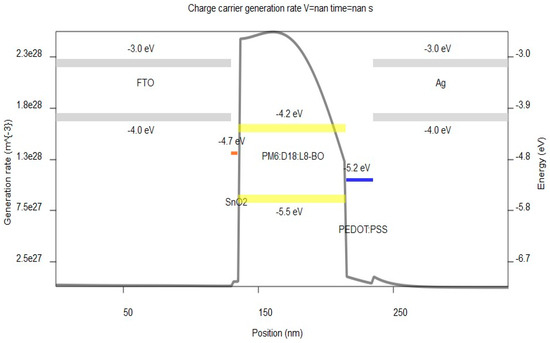
Figure 9.
Charge carrier generation rate as a function of position.
These parameters are directly affected by several factors, including photon absorption, exciton generation and diffusion, dissociation, transport, and the collection of charge carriers by the electrodes. Figure 5 and Figure 6 display the distribution of the incident photon and absorbed photon spectra, respectively. The observed EQE curve in Figure 4b demonstrates a significant absorption of incident photons from 530 nm to 810 nm. This range is particularly important due to the presence of a crucial photon density localized between 350 nm and 880 nm. For the optimal thickness of the active blend (80 nm), the absorption of light is approximately 90%, accompanied by an average generation rate of 2 × 1020 cm−3 s−1.
A broader range of light absorption is caused by the increase in the active blend thickness, hence increasing the likelihood of exciton formation. Consequently, this enhances the Jsc. It is worth noting that the OSC with a thickness of 50 nm has somewhat higher mobility compared to the devices with thicknesses of 80 nm and 250 nm. Additionally, the OSC with a thickness of 50 nm exhibits a Voc of 0.899 V.
In the field of solid-state physics and semiconductors, carrier production and carrier recombination are basic phenomena connected to mobile charge carriers (electrons and electron holes). The carrier generation process involves electrons accumulating energy and migrating from the valence band (where they are generally present) to the conduction band. When an electron absorbs energy (due to interactions with other electrons, photons, or lattice vibrations), it can move freely in the conduction band [51].
Simultaneously, it leaves behind a positively charged “hole” in the valence band, which can likewise move like a particle. The electron–hole pair is the primary unit of generation in semiconductors [52].
For carrier recombination, a conduction band electron loses energy and reoccupies the energy state of an electron hole in the valence band. Essentially, it is the reverse process of carrier generation. Recombination can occur due to many reasons, such as collisions, interactions with other carriers, or lattice vibrations [52].
Furthermore, the mobility of charge carriers is impacted by elements like disorder in the material. In disordered solids used as organic semiconductors, weak localization effects (traps) diminish the mean free path and, consequently, carrier mobility. Carrier recombination also influences mobility; efficient recombination leads to longer lived charge carriers [52].
Charge recombination is identified as a primary determinant in the occurrence of Voc loss. The process of charge recombination is contingent upon the mobility of charge carriers. Increased mobility results in enhanced charge extraction and reduced recombination losses, hence resulting in an elevated Voc as indicated by Equations (24) and (25). Therefore, a decrease in thickness results in a decreased charge recombination rate.
This reduction in the recombination rate contributes to the diffusion and dissociation of excitons, ultimately facilitating the transfer of charges across the cascaded energy levels of the blends. Our active blend Eg is around 1.29 eV. The higher the ratio of our charge mobility µe/µh = 1.05 is, the lower the energy losses according to Equation (24).
In addition, we observe from Figure 9 an important generation rate in the LUMO of the donor side of 2.55 × 1028 m−3 and cascading energy levels between the LUMO of the donor and the LUMO of SnO2 to create a passage toward the electrodes for electron transfer. The high Voc attained by our device can be attributed, in some manner, to the strong level of energy, and its high value is a result of efficient electron transfer. SnO2 is compatible with our structure due to its crystallinity, high electron mobility, and conductivity, and it has proven its efficiency in several studies [36,37,38].
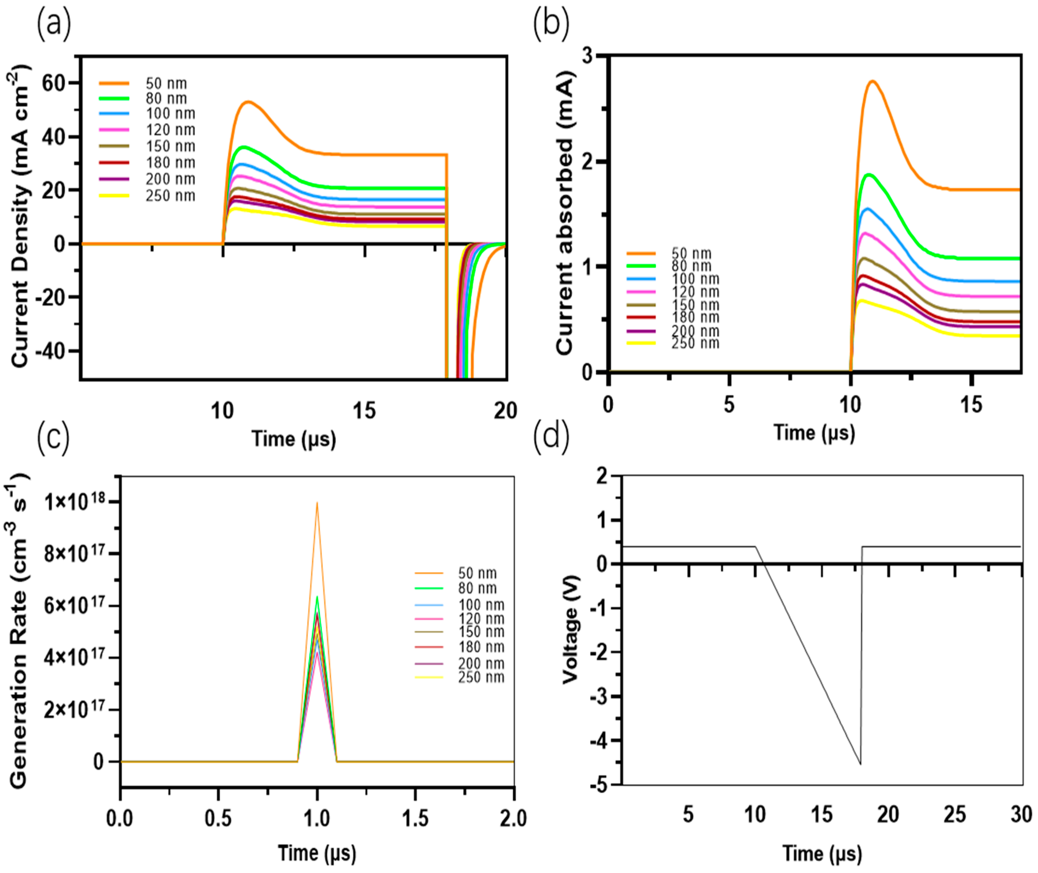
The measurement of charge extraction is conducted using the photo-CELIV. The measurements are depicted in Figure 9. The charge mobilities for all thicknesses (ranging from 50 nm to 250 nm) exhibit a close approximation to 1.451 × 10⁻³ cm2 V−1 s−1, with minimal variation. Figure 10a,b depicts the transient photo-current for various mobilities of the thicknesses. Devices with narrower thicknesses exhibit higher current generation and faster charge extraction compared to devices with wider thicknesses, such as those with thicknesses of 200 nm and 250 nm.

Figure 10.
(a) Transient current density for the different mobilities of the thicknesses of the active layers of different devices; (b) transient current for the different mobilities for all devices; (c) transient generation rate for all devices; and (d) transient voltage for different mobilities for all devices.
These devices with a wider thickness demonstrate slightly lower current generation and slower charge extraction, as illustrated in Figure 10c. The primary factor influencing this behavior is the recombination rate of charges in the wide thickness devices. As previously mentioned, organic materials possess a limited excitons diffusion length, necessitating optimization in the selection of the active surface thickness. Simultaneously, a broad absorption range is required to generate a greater number of excitons while maintaining efficient diffusion and electron passage through the interfaces.
This enhances charge mobilities and facilitates fast charge extraction, ultimately leading to voltage generation and electrode contact (refer to Figure 10d).
Mobility of charges is undoubtedly an important aspect in achieving high-efficiency TOSCs [53]. Electron mobility refers to how quickly electrons flow through a substance when subjected to an electric field. Similarly, hole mobility describes the movement of “holes” (electron vacancies) in the valence band [53]. High mobility allows faster charge transport, resulting to higher gadget performance. Factors impacting mobility include crystal structure, impurities, defects, and temperature [54].
Some materials exhibit low mobility due to their inherent properties; for example, disordered structures like organic semiconductors have random layouts hamper charge flow [53,54]. In addition, the highly doped semiconductors have increased levels of impurities that diminish mobility. Mobility is reduced as temperature declines. Mobility must be balanced with other material qualities (e.g., bandgap, stability). Ternary blends introduce additional interfaces, altering charge mobility [16].
For a high mobility device, proper alignment between D–A energy levels is crucial. In addition, achieving appropriate phase separation among the components is tough [16]. The traps block charge transit, lowering movement, and the efficient charge extraction requires balanced mobility [16].
The recombination prefactor is influenced by various parameters, including the specific recombination mechanism, the mobility of charge, the electric field, and the density of states [25]. The recombination prefactor (Kbi) for our devices was determined by the measurement of various active layer thicknesses. It was observed that a direct relationship exists between the lowering of the active blend thickness and the minimization of the recombination rate of charges, as depicted in Figure 11.
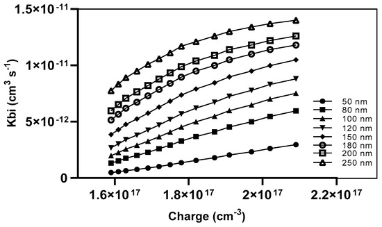
Figure 11.
The Kbi as a function of charge density with different thicknesses.
The application of a 250 nm active layer resulted in a high Kbi of 1.4 × 10⁻¹¹ cm3 s−1 at a charge density of 2.09 × 1017 cm−3. In contrast, a device with a 50 nm thickness achieved a lower Kbi of 2 × 10⁻¹² cm3 s−1 at the same charge density.
Another piece of evidence supports the notion that a broader thickness poses a disadvantage in terms of the distance traveled by charges for extraction, dissociation within the active layer and between interfaces, as well as the transport of charges toward the electrodes.
We conducted a comparative analysis of other theoretical studies performed by Rafiq et al. [55], Ram et al. [56], and Zhu et al. [46], as provided in Table 4. Our analysis focused on the simulation of inverted and direct binary OSCs, as well as direct ternary OSCs, and compared our findings with those of the aforementioned research. The simulation we did showed that single-junction OSCs had a much higher PCE than the results of previous studies shown in Table 4. Additionally, we observed a significant accomplishment in achieving a Jsc of 27.2 mA. This is the highest Jsc value achieved through theoretical work to date. The broadened absorption wavelength of EQE demonstrated by this structure, along with the optimized thickness of the active layer at 80 nm, played a crucial role in facilitating the separation of excitons and the generation of free charge carriers. These factors greatly contributed to the enhancement of the Jsc. Furthermore, our ternary device outperformed the results of Ram et al. and Zhu et al. [46] by achieving a significantly higher Voc value of 82.3 V. Nevertheless, the research conducted by Rafiq et al. demonstrated a greater Voc and FF compared to our TOSC devices, with values of 0.999 V and 88.52%, respectively. Through structural analysis, we have determined that the crucial factor in their successful attainment of Voc and FF lies in the implementation of a triple ETL consisting of C60, PC60BM, and ZnO. This combination has resulted in a tight energy alignment between the LUMO of these materials and a cascading energy level system that promotes efficient electron transfer towards the Ag electrode. However, even though our TOSCs attained a greater Voc and FF, their PCE of 20% surpasses the other research listed in Table 4.
Table 4.
Comparison between our direct and inverted binary OSCs and TOSCs with other simulation studies.
4. Conclusions
We conducted simulations on our devices utilizing an inverted structure consisting of ITO/SnO2/PM6:D18:L8-BO/PEDOT:PSS/Ag. The efficiency results of the device demonstrate a PCE of 20% with the optimization of the active layer thickness at 80 nm. Additionally, it delivers a Voc of 0.89 V, a Jsc of 27.2 mA cm−2, and an FF of 82.3%. These data points position the device among the most noteworthy efficiencies observed thus far in simulated single-junction OSC devices. The active blend was optimized at a thickness of 80 nm, resulting in several enhancements. First, the optimized thickness led to a reduction in the travel distance required for charge carriers to reach the charge transport layers. The utilization of SnO2 has been observed to enhance electron mobility, a critical parameter in reducing energy losses and increasing the Voc, as previously demonstrated in our research findings. Our study highlights the significance of choosing wide-bandgap polymers to enhance light absorption. This entails considering various aspects, such as optical simulation techniques to augment light absorption and minimize reflection, investigating the physical behavior of the cells through electronic and mathematical analyses to identify key parameters, and exploring novel materials, for which the ultimate goal is to develop the efficiency of OSCs.
The primary goal of future research endeavors should be to utilize a global approach to enhance the overall arrangement of OSCs. This entails analyzing various factors, such as utilizing optical engineering techniques to enhance light absorption and minimize reflection, investigating the physical properties of the cells using electronic and mathematical analyses to identify crucial variables, and exploring novel materials and microscopic structures to develop more efficient materials. The main goal is to enhance the efficiency of OSCs. These advancements significantly improved the device’s efficiency.
Author Contributions
Conceptualization, M.E.A.B.; Methodology, M.E.A.B.; Software, M.E.A.B.; Investigation, M.E.A.B.; Writing—original draft, M.E.A.B.; Writing—review & editing, Q.W. and C.Z.; Supervision, C.Z.; Project administration, M.E.A.B. All authors have read and agreed to the published version of the manuscript.
Funding
This work was supported by the National Natural Science Foundation of China (No. 51976157) and the Fundamental Research Funds for the Central Universities.
Institutional Review Board Statement
Not applicable.
Informed Consent Statement
Not applicable.
Data Availability Statement
Data are contained within the article.
Conflicts of Interest
The authors declare no conflicts of interest.
Nomenclature
| q | Elementary charge |
| n | The concentration of free electrons |
| Nc,v | The effective density of states in the conduction band |
| Nt | The number of traps |
| P | The concentration of free holes |
| Jn,p | The current density of the electron and holes |
| vth | The thermal emission velocity of the carriers |
| Ec | Conduction band |
| Ev | Valence band |
| EF,h,e | The energy corresponding to Fermi levels |
| Fn,p | The energy level of the Fermi level in the conduction and valence bands |
| Dn,p | The diffusion coefficient of electrons and holes |
| Rn,p | The recombination rate of electrons and holes |
| G | The carrier generation rate |
| KB | Boltzmann constant |
| T | Temperature |
| Greek Symbols | |
| ε0 | The permittivity of the free space |
| εr | Relative permittivity |
| φ | Voltage profile |
| µe | Electron mobility |
| µh | Hole mobility |
| ΔE | The energy offset |
| η | The normal surface |
| ω | Angular frequency |
| λ | Speed of light |
| Superscript | |
| D | Electron donor |
| A | Electron acceptor |
References
- Chen, L.X. Organic Solar Cells: Recent Progress and Challenges. ACS Energy Lett. 2019, 4, 2537–2539. [Google Scholar] [CrossRef]
- Burke, D.J.; Lipomi, D.J. Green chemistry for organic solar cells. Energy Environ. Sci. 2013, 6, 2053–2066. [Google Scholar] [CrossRef]
- Rhaman, M.M.; Matin, M.A. Organic Solar Cells: Historical developments and challenges. In Proceedings of the 2015 International Conference on Advances in Electrical Engineering (ICAEE), Dhaka, Bangladesh, 17–19 December 2015; pp. 26–29. [Google Scholar] [CrossRef]
- Imamura, S.; Mizutani, T.; Kojima, K.; Ochiai, S. Characteristics and performance of organic photovoltaic cells having the active layer fabricated by ternary organic semiconducting materials. J. Photonics Energy 2011, 1, 011119. [Google Scholar] [CrossRef]
- Farooq, W.; Khan, M.; Khan, A.D. High Performance Bulk-Heterojunction Organic Solar Cells. In Proceedings of the 2019 International Conference on Electrical, Communication, and Computer Engineering (ICECCE), Swat, Pakistan, 24–25 July 2019; pp. 1–6. [Google Scholar] [CrossRef]
- Putnin, T.; Lertvachirapaiboon, C.; Ishikawa, R.; Shinbo, K.; Kato, K.; Ekgasit, S.; Ounnunkad, K.; Baba, A. Enhanced organic solar cell performance: Multiple surface plasmon resonance and incorporation of silver nanodisks into a grating-structure electrode. Opto-Electron. Adv. 2019, 2, 1. [Google Scholar] [CrossRef]
- Würfel, P. Photovoltaic Principles and Organic Solar Cells. Chimia 2007, 61, 770. [Google Scholar] [CrossRef]
- Tadeson, G.; Sabat, R.G. Enhancement of the Power Conversion Efficiency of Organic Solar Cells by Surface Patterning of Azobenzene Thin Films. ACS Omega 2019, 4, 21862–21872. [Google Scholar] [CrossRef] [PubMed]
- Ghosekar, I.C.; Patil, G.C. Review on performance analysis of P3HT:PCBM-based bulk heterojunction organic solar cells. Semicond. Sci. Technol. 2021, 36, 045005. [Google Scholar] [CrossRef]
- Wang, X.; Sun, Q.; Gao, J.; Wang, J.; Xu, C.; Ma, X.; Zhang, F. Recent Progress of Organic Photovoltaics with Efficiency over 17%. Energies 2021, 14, 4200. [Google Scholar] [CrossRef]
- Schlachter, A.; Marineau-Plante, G.; Harvey, P.D.; Agrawal, A.; Sharma, G.D. Efficient ternary bulk heterojunction organic solar cells using a low-cost nonfullerene acceptor. J. Mater. Chem. C 2022, 10, 4372–4382. [Google Scholar] [CrossRef]
- Zhang, S.; Shen, H.; Zhang, X.; Fan, P.; Zhou, B.; Yu, J.; Huang, J. Efficient Ternary Organic Solar Cells with Small Aggregation Phases and Low Bimolecular Recombination Using ICBA: ITIC Double Electron Acceptors. IEEE J. Photovolt. 2018, 8, 171–176. [Google Scholar] [CrossRef]
- Ma, Q.; Jia, Z.; Meng, L.; Zhang, J.; Zhang, H.; Huang, W.; Yuan, J.; Gao, F.; Wan, Y.; Zhang, Z.; et al. Promoting charge separation resulting in ternary organic solar cells efficiency over 17.5%. Nano Energy 2020, 78, 105272. [Google Scholar] [CrossRef]
- Doumon, N.Y.; Yang, L.; Rosei, F. Ternary organic solar cells: A review of the role of the third element. Nano Energy 2022, 94, 106915. [Google Scholar] [CrossRef]
- Ma, R.; Yan, C.; Yu, J.; Liu, T.; Liu, H.; Li, Y.; Chen, J.; Luo, Z.; Tang, B.; Lu, X.; et al. High-Efficiency Ternary Organic Solar Cells with a Good Figure-of-Merit Enabled by Two Low-Cost Donor Polymers. ACS Energy Lett. 2022, 7, 2547–2556. [Google Scholar] [CrossRef]
- Zhang, T.; Gasparini, N. Ternary organic solar cells: Insights into charge and energy transfer processes. Appl. Phys. Lett. 2022, 120, 250501. [Google Scholar] [CrossRef]
- Xu, X.; Li, Y.; Peng, Q. Ternary Blend Organic Solar Cells: Understanding the Morphology from Recent Progress. Adv. Mater. 2022, 34, 2107476. [Google Scholar] [CrossRef] [PubMed]
- Lin, Y.; Adilbekova, B.; Firdaus, Y.; Yengel, E.; Faber, H.; Sajjad, M.; Zheng, X.; Yarali, E.; Seitkhan, A.; Bakr, O.M.; et al. 17% Efficient Organic Solar Cells Based on Liquid Exfoliated WS2 as a Replacement for PEDOT:PSS. Adv. Mater. 2019, 31, 1902965. [Google Scholar] [CrossRef] [PubMed]
- Duan, X.; Song, W.; Qiao, J.; Li, X.; Cai, Y.; Wu, H.; Zhang, J.; Hao, X.; Tang, Z.; Ge, Z.; et al. Ternary strategy enabling high-efficiency rigid and flexible organic solar cells with reduced non-radiative voltage loss. Energy Environ. Sci. 2022, 15, 1563–1572. [Google Scholar] [CrossRef]
- Feng, H.; Dai, Y.; Guo, L.; Wang, D.; Dong, H.; Liu, Z.; Zhang, L.; Zhu, Y.; Su, C.; Chen, Y.; et al. Exploring ternary organic photovoltaics for the reduced nonradiative recombination and improved efficiency over 17.23% with a simple large-bandgap small molecular third component. Nano Res. 2022, 15, 3222–3229. [Google Scholar] [CrossRef]
- Overview. Talk overview • History • Overview of model • Electrical models • Drift Diffusion • Circuit Model • Optical Models. • Exciton Models • Simulation Modes • Thermal Models. Available online: https://www.oghma-nano.com (accessed on 8 June 2024).
- Lewińska, G. Ternary Organic Solar Cells—Simulation–Optimization Approach. Electron. Mater. Lett. 2024, 20, 440–449. [Google Scholar] [CrossRef]
- Bensenouci, S.; Rahmoun, K.; Aissat, A. Electrical simulation and optimization of organic photovoltaic cells based PTB7:PC70BM. J. Ovonic Res. 2024, 20, 163–175. [Google Scholar] [CrossRef]
- Li, W.; Zeiske, S.; Sandberg, O.J.; Riley, D.B.; Meredith, P.; Armin, A. Organic solar cells with near-unity charge generation yield. Energy Environ. Sci. 2021, 14, 6484–6493. [Google Scholar] [CrossRef]
- Zhou, N.; Facchetti, A. Charge Transport and Recombination in Organic Solar Cells (OSCs). In Organic and Hybrid Solar Cells; Huang, H., Huang, J., Eds.; Springer International Publishing: Cham, Switzerland, 2014; pp. 19–52. [Google Scholar] [CrossRef]
- Tara, A.; Bharti, V.; Sharma, S.; Gupta, R. Harnessing the Role of Charge Transport Layers for Efficient Design of PBDBT/ITIC-OE Based Organic Solar Cell. Trans. Electr. Electron. Mater. 2023, 24, 356–364. [Google Scholar] [CrossRef]
- Xu, H.; Yuan, F.; Zhou, D.; Liao, X.; Chen, L.; Chen, Y. Hole transport layers for organic solar cells: Recent progress and prospects. J. Mater. Chem. A 2020, 8, 11478–11492. [Google Scholar] [CrossRef]
- Agnihotri, P.; Sahu, S.; Tiwari, S. Recent advances & perspectives in electron transport layer of organic solar cells for efficient solar energy harvesting. In Proceedings of the 2017 International Conference on Energy, Communication, Data Analytics and Soft Computing (ICECDS), Chennai, India, 1–2 August 2017; pp. 1568–1573. [Google Scholar] [CrossRef]
- Bin, H.; Wang, J.; Li, J.; Wienk, M.M.; Janssen, R.A.J. Efficient Electron Transport Layer Free Small-Molecule Organic Solar Cells with Superior Device Stability. Adv. Mater. 2021, 33, 2008429. [Google Scholar] [CrossRef] [PubMed]
- Xu, Y.; Zhou, H.; Duan, P.; Shan, B.; Xu, W.; Wang, J.; Liu, M.; Zhang, F.; Sun, Q. Improving the Efficiency of Organic Solar Cells with Methionine as Electron Transport Layer. Molecules 2022, 27, 6363. [Google Scholar] [CrossRef] [PubMed]
- Jin, F.; Peng, R.; Qiu, Y.; Zhang, J.; Ge, Z. Highly Efficient and Stable Organic Solar Cells Enabled by a PEDOT:PSS/HxMoO3 Hybrid Hole Transport Layer. ACS Appl. Energy Mater. 2023, 6, 9532–9542. [Google Scholar] [CrossRef]
- Yin, P.; Yin, Z.; Ma, Y.; Zheng, Q. Improving the charge transport of the ternary blend active layer for efficient semitransparent organic solar cells. Energy Environ. Sci. 2020, 13, 5177–5185. [Google Scholar] [CrossRef]
- Yao, J.; Qiu, B.; Zhang, Z.-G.; Xue, L.; Wang, R.; Zhang, C.; Chen, S.; Zhou, Q.; Sun, C.; Yang, C.; et al. Cathode engineering with perylene-diimide interlayer enabling over 17% efficiency single-junction organic solar cells. Nat. Commun. 2020, 11, 2726. [Google Scholar] [CrossRef] [PubMed]
- Tang, H.; Bai, Y.; Zhao, H.; Qin, X.; Hu, Z.; Zhou, C.; Huang, F.; Cao, Y. Interface Engineering for Highly Efficient Organic Solar Cells. Adv. Mater. 2024, 36, 2212236. [Google Scholar] [CrossRef]
- Fu, J.; Fong, P.W.K.; Liu, H.; Huang, C.-S.; Lu, X.; Lu, S.; Abdelsamie, M.; Kodalle, T.; Sutter-Fella, C.M.; Yang, Y.; et al. 19.31% binary organic solar cell and low non-radiative recombination enabled by non-monotonic intermediate state transition. Nat. Commun. 2023, 14, 1760. [Google Scholar] [CrossRef] [PubMed]
- Kong, T.; Wang, R.; Zheng, D.; Yu, J. Modification of the SnO2 Electron Transporting Layer by Using Perylene Diimide Derivative for Efficient Organic Solar Cells. Front. Chem. 2021, 9, 703561. [Google Scholar] [CrossRef] [PubMed]
- Niederhausen, J.; Mazzio, K.A.; MacQueen, R.W. Inorganicorganic interfaces in hybrid solar cells. Electron. Struct. 2021, 3, 33002. [Google Scholar] [CrossRef]
- Di Mario, L.; Garcia Romero, D.; Wang, H.; Tekelenburg, E.K.; Meems, S.; Zaharia, T.; Portale, G.; Loi, M.A. Outstanding Fill Factor in Inverted Organic Solar Cells with SnO2 by Atomic Layer Deposition. Adv. Mater. 2024, 36, 2301404. [Google Scholar] [CrossRef] [PubMed]
- Tian, H.; Ni, Y.; Zhang, W.; Xu, Y.; Zheng, B.; Jeong, S.Y.; Wu, S.; Ma, Z.; Du, X.; Hao, X.; et al. Over 19.2% efficiency of layer-by-layer organic photovoltaics enabled by a highly crystalline material as an energy donor and nucleating agent. Energy Environ. Sci. 2024, 17, 5173–5182. [Google Scholar] [CrossRef]
- Jiang, Y.; Sun, S.; Xu, R.; Liu, F.; Miao, X.; Ran, G.; Liu, K.; Yi, Y.; Zhang, W.; Zhu, X. Non-fullerene acceptor with asymmetric structure and phenyl-substituted alkyl side chain for 20.2% efficiency organic solar cells. Nat. Energy 2024, 1–12. [Google Scholar] [CrossRef]
- Chen, L.; Yi, J.; Ma, R.; Pena, T.A.D.; Luo, Y.; Wang, Y.; Wu, Y.; Zhang, Z.; Hu, H.; Li, M.; et al. 19% efficiency in organic solar cells of Benzo [1,2-b:4,5-b′]Difuran-based donor polymer realized by volatile + non-volatile dual-solid-additive strategy. Mater. Sci. Eng. R Rep. 2024, 159, 100794. [Google Scholar] [CrossRef]
- Guan, S.; Li, Y.; Xu, C.; Yin, N.; Xu, C.; Wang, C.; Wang, M.; Xu, Y.; Chen, Q.; Wang, D.; et al. Self-Assembled Interlayer Enables High-Performance Organic Photovoltaics with Power Conversion Efficiency Exceeding 20%. Adv. Mater. 2024, 36, 2400342. [Google Scholar] [CrossRef] [PubMed]
- MacKenzie, R.C.I.; Shuttle, C.G.; Dibb, G.F.; Treat, N.; von Hauff, E.; Robb, M.J.; Hawker, C.J.; Chabinyc, M.L.; Nelson, J. Interpreting the Density of States Extracted from Organic Solar Cells Using Transient Photocurrent Measurements. J. Phys. Chem. C 2013, 117, 12407–12414. [Google Scholar] [CrossRef]
- Deschler, F.; Riedel, D.; Ecker, B.; von Hauff, E.; Da Como, E.; MacKenzie, R.C.I. Increasing organic solar cell efficiency with polymer interlayers. Phys. Chem. Chem. Phys. 2013, 15, 764–769. [Google Scholar] [CrossRef] [PubMed]
- MacKenzie, R.C.I.; Shuttle, C.G.; Chabinyc, M.L.; Nelson, J. Extracting Microscopic Device Parameters from Transient Photocurrent Measurements of P3HT:PCBM Solar Cells. Adv. Energy Mater. 2012, 2, 662–669. [Google Scholar] [CrossRef]
- Zhu, L.; Zhang, M.; Xu, J.; Li, C.; Yan, J.; Zhou, G.; Zhong, W.; Hao, T.; Song, J.; Xue, X.; et al. Single-junction organic solar cells with over 19% efficiency enabled by a refined double-fibril network morphology. Nat. Mater. 2022, 21, 656–663. [Google Scholar] [CrossRef]
- Liu, J.; Liu, X.; Xin, J.; Zhang, Y.; Wen, L.; Liang, Q.; Miao, Z. Dual Function of the Third Component in Ternary Organic Solar Cells: Broaden the Spectrum and Optimize the Morphology. Small 2024, 20, 2308863. [Google Scholar] [CrossRef] [PubMed]
- Liang, Q.; Duan, M.; Geng, Z.; Zhang, M.; Xu, W.; Geng, H.; He, Z.; Liu, J. Regulation of molecular orientation in organic solar cells. Chem. Eng. J. 2024, 488, 150783. [Google Scholar] [CrossRef]
- Xin, J.; Zhao, C.; Geng, Z.; Xue, W.; Chen, Z.; Song, C.; Yan, H.; Liang, Q.; Miao, Z.; Ma, W.; et al. Elucidate the Thermal Degradation Mechanism of Y6-Based Organic Solar Cells by Establishing Structure-Property Correlation. Adv. Energy Mater. 2024, 2401433. [Google Scholar] [CrossRef]
- Mohamed El Amine, B.; Zhou, Y.; Li, H.; Wang, Q.; Xi, J.; Zhao, C. Latest Updates of Single-Junction Organic Solar Cells up to 20% Efficiency. Energies 2023, 16, 3895. [Google Scholar] [CrossRef]
- Deskins, N.A.; Rao, P.M.; Dupuis, M. Charge Carrier Management in Semiconductors: Modeling Charge Transport and Recombination. In Springer Handbook of Inorganic Photochemistry; Springer: Cham, Switzerland, 2022; pp. 365–398. [Google Scholar] [CrossRef]
- Mozer, A.J.; Dennler, G.; Sariciftci, N.S.; Westerling, M.; Pivrikas, A.; Österbacka, R.; Juška, G. Time-dependent mobility and recombination of the photoinduced charge carriers in conjugated polymer/fullerene bulk heterojunction solar cells. Phys. Rev. B Condens. Matter Mater. Phys. 2005, 72, 035217. [Google Scholar] [CrossRef]
- Gasparini, N.; Salleo, A.; McCulloch, I.; Baran, D. The role of the third component in ternary organic solar cells. Nat. Rev. Mater. 2019, 4, 229–242. [Google Scholar] [CrossRef]
- Wang, K.; Sun, C.; Zhang, C.; Bai, H.; Sang, S.; Li, Y.; Chen, Z.; Li, X.; Meng, L.; Li, Y. Fine-tuning of film morphology through addition of a third component enables organic solar cells with efficiency over 18%. Mater. Chem. Front. 2024. [Google Scholar] [CrossRef]
- Rafiq, M.; Haider, M.; Li, H.; Yang, J. Precise control of hole transport layer integration on PDTS-DTTFBT: PC71BM organic solar cells. Phys. Scr. 2024, 99, 055903. [Google Scholar] [CrossRef]
- Ram, K.S.; Singh, J. Over 20% Efficient and Stable Non-Fullerene-Based Ternary Bulk-Heterojunction Organic Solar Cell with WS2 Hole-Transport Layer and Graded Refractive Index Antireflection Coating. Adv. Theory Simul. 2020, 3, 2000047. [Google Scholar] [CrossRef]


Disclaimer/Publisher’s Note: The statements, opinions and data contained in all publications are solely those of the individual author(s) and contributor(s) and not of MDPI and/or the editor(s). MDPI and/or the editor(s) disclaim responsibility for any injury to people or property resulting from any ideas, methods, instructions or products referred to in the content. |
© 2024 by the authors. Licensee MDPI, Basel, Switzerland. This article is an open access article distributed under the terms and conditions of the Creative Commons Attribution (CC BY) license (https://creativecommons.org/licenses/by/4.0/).