Article

Low Temperature Pyrolysis and Exfoliation of Waste Printed Circuit Boards: Recovery of High Purity Copper Foils

by
Elanjikkal Indran Anjana
1,2,
Kalidoss Jayasankar
1,*,
Rita Khanna
3,*,
Jayapalan Venkatesan
1,
Yury V. Konyukhov
4 and
Partha Sarathy Mukherjee
5
1
Materials Science & Technology Division, CSIR-National Institute for Interdisciplinary Science and Technology, Thiruvananthapuram 695019, India
2
Academy of Scientific and Innovative Research (AcSIR), Ghaziabad 201002, India
3
School of Materials Science and Engineering (Ret.), The University of New South Wales, Sydney 2052, Australia
4
Department of Enrichment and Processing of Minerals and Technogenic Raw Materials, National University of Science and Technology “MISIS”, Moscow 119049, Russia
5
Institute of Minerals and Materials Technology (Ret.), Council of Scientific and Industrial Research, Bhubaneshwar 751013, India
*
Authors to whom correspondence should be addressed.
Sustainability 2024, 16(15), 6269; https://doi.org/10.3390/su16156269
Submission received: 20 June 2024 / Revised: 14 July 2024 / Accepted: 19 July 2024 / Published: 23 July 2024

Abstract

:
Although several techniques have been developed to extract copper from waste printed circuit boards (PCBs), there remain several challenges regarding energy consumption, local area contamination and environmental damage. A novel technique has been developed for extracting copper foils from waste PCBs based on low temperature pyrolysis followed by exfoliation to overcome these issues. The standard pretreatment steps of removing electronic components from PCBs and mechanical processing/size-reduction/powdering, etc., were minimized in this study. Several unsorted ‘as received’ PCBs were heat treated in the temperature range 750–850 °C for 5–20 min. in an argon atmosphere. Brittle dark chars and other residues on the heat-treated specimens were scrapped off to separate copper foils and other residuals. Most of the electronic components mounted on PCBs had dropped off during the heat treatment. Good-quality copper foils were recovered in all cases; the purity of copper was in excess of 85 wt.%. Key impurities present were Pb, Sn and Zn with typical concentrations less than 4 wt.%. Key features of the technique include minimizing energy intensive pre-treatment processes and waste handling, low pyrolysis temperatures and short heating times. This energy-efficient approach has the potential to enhance resource recovery while reducing the loss of materials, local area contamination and pollution near e-waste processing facilities.

1. Introduction

Electronic waste (e-waste) refers to discarded end-of-life electrical and electronic equipment with little further utility and is currently amongst the fastest growing solid waste streams in the world. Short lifespans, technological advancements and regular upgrades of electronic equipment such as smart phones, mobile devices, TVs, computers, laptops, notebooks, etc., generate large amounts of e-waste. Currently, one cannot imagine life without smartphones or mobile phones; the number of mobile users worldwide is projected to reach 7.49 billion by 2025 [1]. In 2021, the number of mobile devices operating globally was ~15 billion and this is expected to reach 18.2 billion by 2025 [2]. With an annual growth rate of 3 to 5%, nearly 53.6 Mt (million tons) of e-waste was generated globally in 2019 and this could reach 74.7 Mt by 2030 [3]. Among these, the third highest volumes of e-waste (3.2 Mt) were generated in India [4]. Even though e-waste has huge potential as a secondary material resource with over 57 billion USD of contained value, the recycling rates continue to be somewhat limited and low (~17.4%) [5,6]. There is an urgent need to enhance the recovery of metals and other valuable materials from e-waste. A critical evaluation of the current e-waste recycling approaches, their energy efficiency, environmental and economic sustainability is becoming increasingly important.
Recycling of e-waste typically involves collection, physical sorting, the removal of hazardous materials, electronic components, mechanical pre-treatments and end-stage processing using a number of techniques such as acid leaching, electrolysis, pyrometallurgical, hydrometallurgical, bio-metallurgical routes, etc. [7,8,9,10,11]. Among these, pyrolysis that involves heat treatment in a closed inert atmosphere has been used extensively for resource recovery from waste PCBs [12,13]. While low temperature pyrolysis (up to 600 °C) is used to recover organics, polymers and associated biproducts [14], much higher temperatures (>750 °C) are required for recovering copper, precious metals and ceramic-based products [15]. The use of pyrolysis for the processing of waste PCBs for resource recovery has been critically reviewed in the literature [16,17,18]. Microwave pyrolysis has also been proposed as an effective method for metal recovery from waste PCBs, highlighting its potential as a pretreatment process [19].
Several e-waste processing techniques have achieved a certain level of maturity and commercialization [20,21]. However, the resource recovery from electronic waste continues to have a significant environmental footprint and social impact especially in poor and developing regions of the world [22]. Traditional mineral processing approaches are still being used for recycling e-waste with very little modifications. This issue is further aggravated by illegal operations, trans-boundary movements, limited safety regulations, semi-skilled labour and inadequate infrastructure [23]. In the informal sector, small- and large-scale operators try to recover materials in the cheapest way possible, while disposing of residual materials by discharging then into waterways, burning them or dumping them in landfills [24]. As several valuables present in e-waste could be destroyed/wasted through inappropriate handling in the unorganized sector worldwide, efficient and sustainable recovery of material resources and safe disposal of e-waste assumes great significance.
In this article we focus our attention on the recovery of copper from waste printed circuit boards (PCBs). Copper is the primary metallic element present in waste PCBs, with concentrations ranging between 10 and 25 wt.%; these concentrations are several times higher those present in natural ores [25,26]. A variety of techniques have been used for extracting copper from waste PCBs. Hydrometallurgical techniques typically involve mechanical processing and crushing/powdering followed by chemical leaching to extract copper [27]. Copper leaching is carried out using acid leaching, chloride leaching and ammonia–ammonium salts leaching with H2SO4/H2O2, HNO3 and CuSO4-NaCl-H2SO4 as leaching agents, among others [28]. Wu et al. [29] investigated the bioleaching of copper from waste PCBs using a cultural supernatant of iron sulphur oxidizing bacteria; 93.4% of copper was recovered in total from 100 g/L PCB concentrates in 9 days. Bioleaching on large pieces of waste PCBs was attempted by Adhapure et al. [30]; extraction of metals by bacteria required a prior chemical treatment of waste PCBs. Jujun et al. [31] used a hybrid technology using physical and biological methods involving crushing/grinding, corona–electrostatic separation and bioleaching.
A number of pyrometallurgical investigations have reported on extracting copper from waste PCBs, e.g., heat treatment at 550 °C for 2 h in vacuum [32]; a multi-stage pyrometallurgical approach with heat treatment at 1200 °C in inert atmosphere to recover metallic copper and copper slag [33]; a corona–electrostatic separator to separate metallic and non-metallic PCB powders and vacuum pyrolysis at 850 °C [34]; and heat treatments at temperatures ranging from 800 °C to 1550 °C in inert atmosphere for 20 min to recover copper and copper–lead–tin alloys [20,35], among others. Other approaches include supercritical water oxidation of PCBs and an electrokinetic process [36], electrochemical oxidation of PCBs without any mechanical processing [37], etc.
While generally achieving high copper recovery rates, most techniques require significant amounts of initial processing that require a great deal of effort, manpower, energy, infrastructure, etc., along with being a source of local area pollution. Hydrometallurgical approaches produce secondary waste in the form of spent acids, residues, etc., and are economically inefficient for commercial-scale operations [38]. Biometallurgical approaches are very slow; significant developments will be required before these techniques become commercially viable. In the pyrometallurgical approaches, the generation of harmful dioxins, furans and brominated compounds can be a serious issue during low temperature pyrolysis of waste PCBs [39]; however, these emissions become negligible at temperatures above 700 °C [40].
As copper is a high-volume valuable resource, it is important to develop optimal PCB recycling approaches that will significantly enhance copper recovery with minimal energy consumption, local area contamination and environmental damage. A novel approach based on low temperature pyrolysis followed by exfoliation is presented in this study.

Aim of the Investigation

This study seeks to develop a novel approach for extracting copper foils from several ‘as-received’ waste PCBs with minimal handling and/or pretreatment and energy consumption. Using an innovative route, the key process steps in removing electronic components from PCBs and mechanical processing, including size reduction, powdering, etc., will be minimized to a great extent. Using low temperature pyrolysis followed by exfoliation, operating temperatures and heating times will be optimized towards maximal resource recovery while ensuring no harmful dioxins/furans are released during the process. An in-depth analysis of the results will be carried out in terms of the quality and amounts of copper foils recovered. Significant reduction in mechanical pre-treatments on waste PCBs, a standard feature of most e-waste recycling approaches, is a key innovation of this study.

2. Background

Basic information about the structural features of PCBs and typical mechanical pre-treatments are outlined next with the aim of developing a deeper understanding prior to the development of strategies for recycling and resource recovery from waste PCBs.

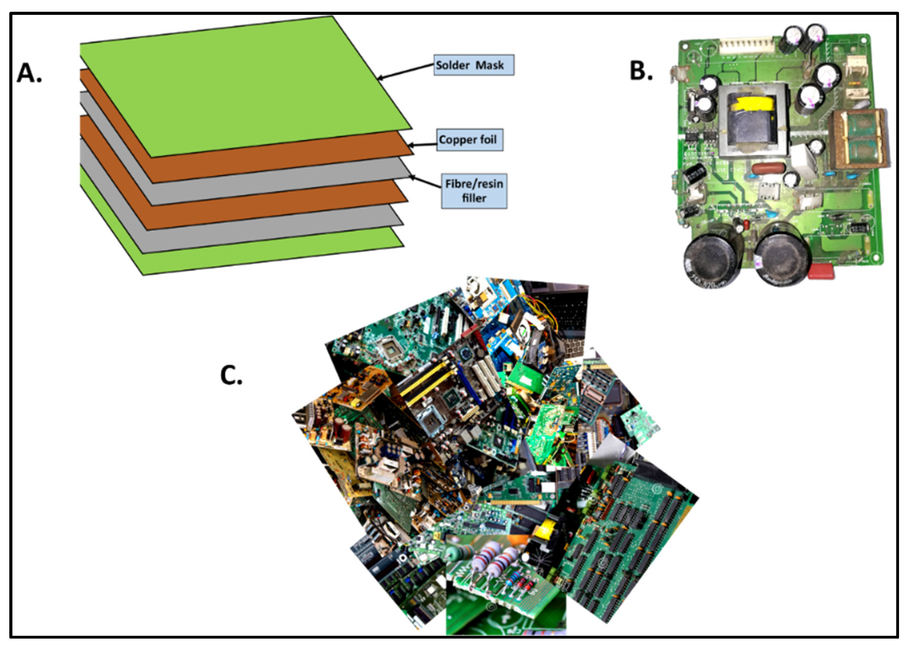
2.1. Structural Features of PCBs

The general purpose of a PCB, the central part providing functionality in most electronic devices, is to provide mechanical support for connecting requisite electronic components on a rigid/flexible substrate. PCBs typically consist of conducting copper layers bonded together with non-conducting fibreglass/epoxy resin fillers (Figure 1A). PCBs can be single/double/or multilayered depending on the power requirements of the device; up to 50 copper layers have been used in some high-performance applications [41]. The FR-4 is the most common dielectric material used in PCBs, where FR stands for fire retardant and the 4 is its grade compared to other glassy laminates. Copper is present in the form of foils in these PCBs, and its relative proportion can be up to 15–20 wt.%. The metallic grade of high purity copper present in PCBs can sometimes be up to one hundred times that in natural mineral resources [42,43]. Figure 1 shows a typical PCB without and with electronic components and a collection of waste PCBs as present in the e-waste collected from different sources. Copper foils are present primarily in the PCB substrate; some copper is also present in the wiring and connections [44].

2.2. Mechanical Pre-Treatments

Special pre-treatments required for copper recovery from waste PCBs involve disassembly for removing electronic components, and mechanical treatments such as crushing, grinding, size reduction, sorting, powdering, etc. [45,46]. These two aspects are discussed next. The removal of electronic components (ECs) is usually one of the first steps of PCB disassembly and may be carried out either manually or automatically [47]. ECs such as integrated circuits, resistors, capacitors, switches, LEDs, etc., are used to carry out device functions/operations and may contain different types of metals, ceramics and other constituents over a wide composition range [48]. ECs are usually soldered or welded to the printed circuit boards; some of these may also be attached through fastenings, wrapping with screws, clinks, rivets, etc., and would require selective disassembly for their removal [49]. The removal of ECs is carried out by melting solders with infrared heaters, hot fluids, electronic heating tubes, hot air; mechanically breaking solder joints with hammers, grinders, gas jets, etc.; or chemical etching with diesel, acids, paraffin oils, electrodynamic fragmentation, etc. [50,51,52]. Removed ECs can sustain extensive damage during these processes and are unlikely to be reused in most cases except as a materials resource.
The second key pretreatment step involves a reduction in the size of PCBs through shredding (up to 50 mm), hammer grinding (up to 2.5 mm), vibrating screens, cyclones, magnetic separators, etc. [53]. The crushing of boards may sometimes require specialist equipment depending on the crushing efficiency, hardness and tenacity of various constituents, and requisite energy consumption [54,55]. Swing hammers are used for industrial-scale processing [56]; low-temperature ball mills are used to break PCBs into nanosized particles [57]. Abrasive water jets have also been used to cut the hard structure of PCBs and to reduce sizes from 14 mm down to 1 mm [58]. Such mechanical and physical processing of waste PCBs can release dust and fine powders including heavy metals such as Cr, Cu, Cd, Pb in and around the recycling areas and may also generate high level noise [59]. Some of the pollutants become dispersed through the surrounding air into regions neighbouring the processing areas. Contaminants, hazardous elements, and heavy metals can enter waterways as well as ground soil or may become partially airborne causing significant environmental damage [60]. Direct human exposure to these contaminants can have irreversible, short- and long-term health effects in the populace in affected regions. A reduction in the number of process steps, adequate safety procedures during dismantling and mechanical processing has the potential to reduce local area contamination and pollution near e-waste processing facilities.

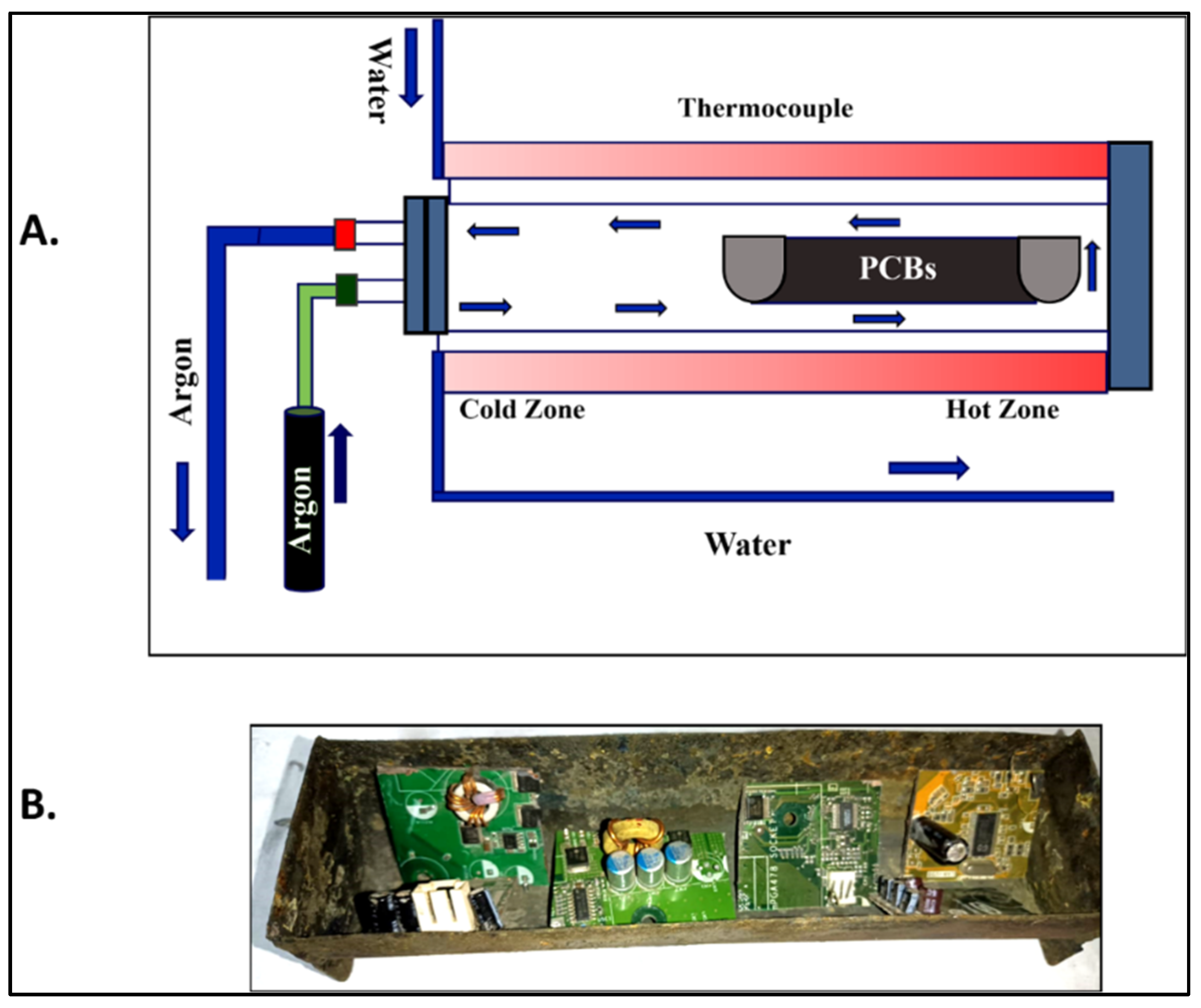
3. Experimental Section

A large number of waste PCBs were sourced from local e-waste recyclers and suppliers. These were in a range of shapes, types and sizes. These were cut into approximately 3 cm × 3 cm pieces; this cutting was required due to the size limitations of the crucible used and furnace dimensions. Such cutting may not be necessary in large scale furnaces or during commercial scale waste recycling.
A schematic representation of the furnace used is given in Figure 2A; an inconel crucible loaded with several pieces of ‘as-received’ PCBs is shown in Figure 2B. A high temperature tubular resistance furnace (8.5 cm dia., 80.7 cm long) was used for the pyrolysis of waste PCBs. Approximately 60 g of PCB pieces were loaded into a semi-cylindrical inconel crucible (5.5 cm dia., 21 cm long) and the assembly was placed in the furnace. The furnace was sealed at both ends and was purged with pure argon. It was then filled with argon and sealed; there was no continuous flow of gas during the heat treatment. The outer shell of the furnace was continuously water cooled during the treatment procedure. The furnace was heated at the rate of 20 °C/min until the set temperatures (750 °C, 800 °C, 850 °C) were reached. Thermal profile was uniform in the hot zone of the furnace; temperatures were significantly lower in the cold zone of the furnace. These temperatures were chosen to ensure the complete destruction of harmful dioxins/furans/brominated products generated during the thermal treatment of waste PCBs [61]. Heat treatments were carried out for 5, 10 and 20 min and the power to the furnace was then switched off. The heat-treated specimens were furnace cooled and then taken out for further analysis. Experiments were repeated at least three times for each set of operating conditions. In addition to enhancing the reproducibility of results, such repetitions can compensate to some extent the initial variability in raw waste specimens. The deviations in the results were found to be within ±5%.
Weight loss was recorded during the heat treatments in all cases; weights of various constituents of pyrolysis residues were also recorded. Detailed investigations were carried out on the copper foils using techniques such as Scanning Electron Microscopy (SEM)/Energy Dispersive Spectroscopy (EDS) on Zeiss EVO 180 model SEM/EDS; optical microscopy with Lecia DMRX microscope attached to a Leica DFC 420 camera and the Leica LAS 3.8 software; and the Inductively Coupled Plasma Optical Emission Spectrometry and Mass spectroscopy (ICP-MS) technique. The XRD data were collected using Cu Kα radiation (45 KV, 40 mA) in the angular range 10–90°, with a step size of 0.2° and a time step of 20 s. Detailed results from the investigation are presented next in the following section.

4. Results

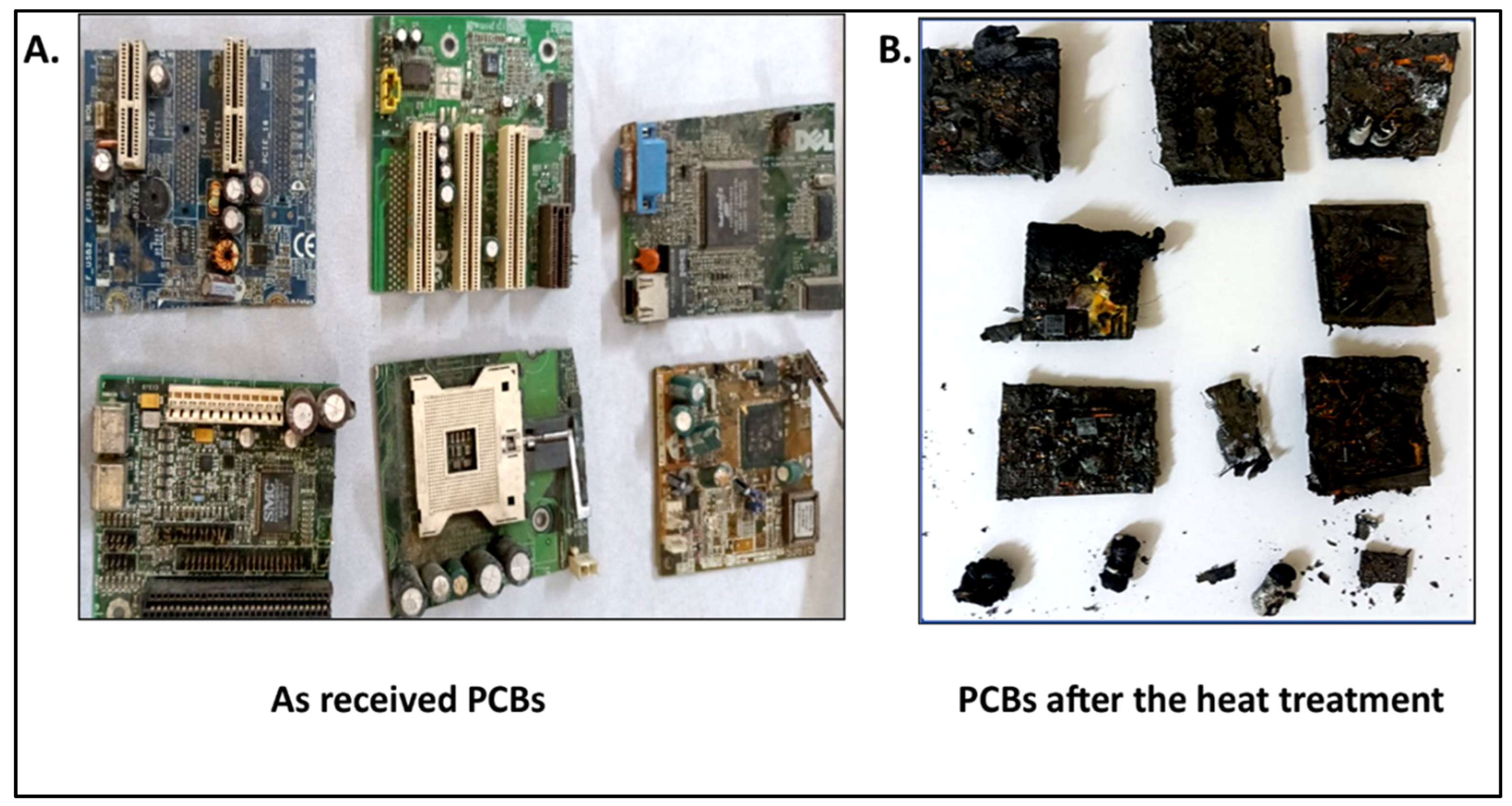
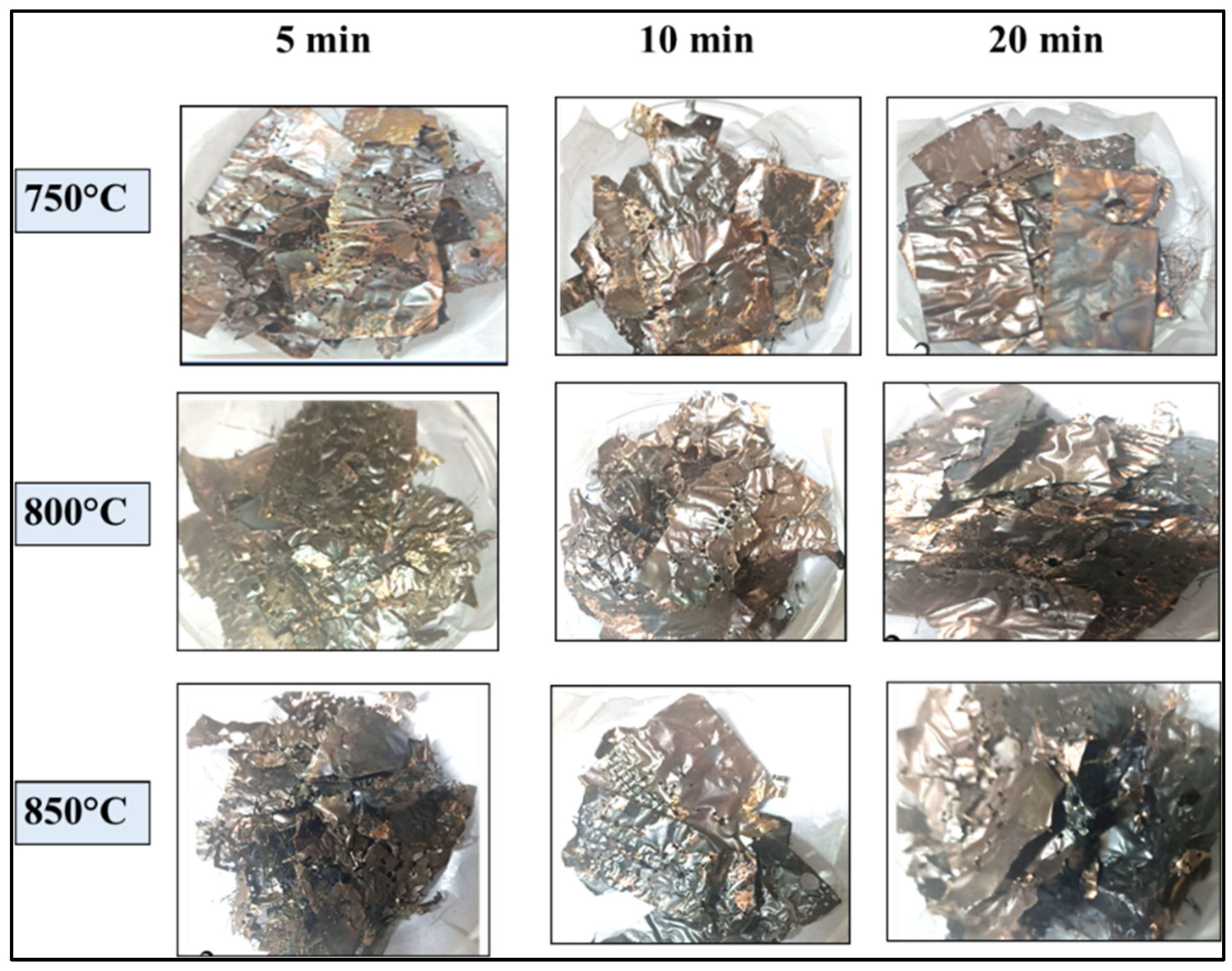
4.1. Morphology of PCBs after Pyrolysis

A representative example of PCBs before and after the heat treatments is shown in Figure 3. Please note that these images are not to scale.
Brittle dark chars/residues on the heat-treated specimens were manually scraped off to separate them into copper foils and other residuals (Figure 4). The key constituents of the residuals were found to be fibreglass sheets, copper foils, chars, wires, component fragments, etc. The attention here was focussed specifically on the recovery of copper. The extraction of other metals, precious as well as base metals, rare earth elements, etc., that are likely to be concentrated in the other residuals fraction (Figure 4B), will be reported elsewhere. Copper foils were subjected further to ultrasonic cleaning to remove surface impurities; a few examples of clean copper foils after ethanol sonification for 30 min are shown in Figure 4C.

4.2. Net Weight Loss after Pyrolysis

Weights were recorded for PCBs before and after the heat treatments. The net weight loss after the heat treatments can be attributed to the thermal degradation of polymers present in the PCBs and their release in the gaseous phase. The polymer content in the PCBs that was lost during pyrolysis, as estimated from the net weight lost, has been plotted in Figure 5 for a range of temperatures and processing times. These amounts were found to range between 23.0 and 28.5 wt.% with marginal variations across different operating conditions; observed variations can be attributed to inherent compositional variations in waste PCBs. This trend is to be expected as all polymers present in waste PCBs are likely to completely degrade by ~600 °C [62]. Therefore, small changes are to be expected at higher temperatures and processing times.

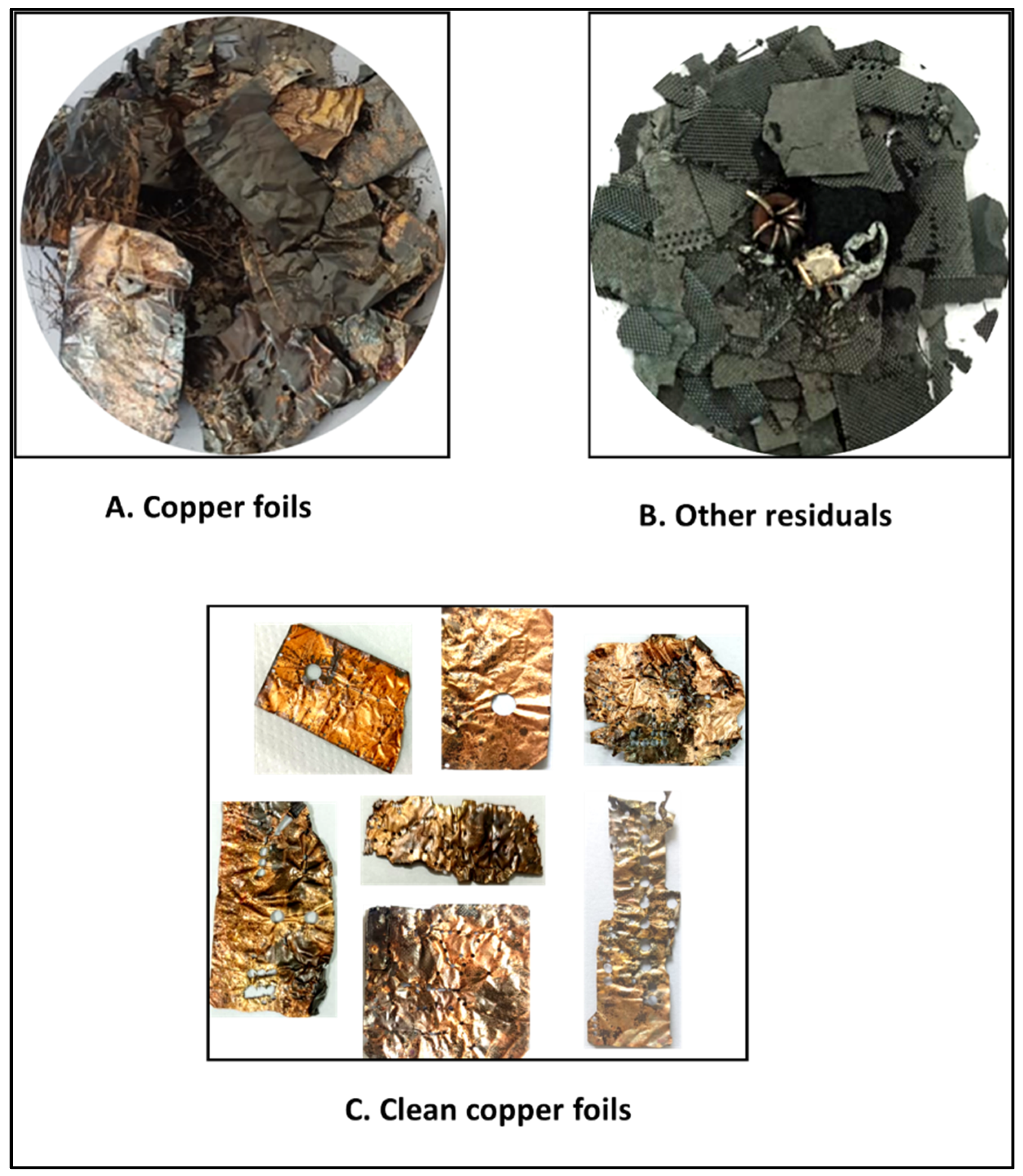
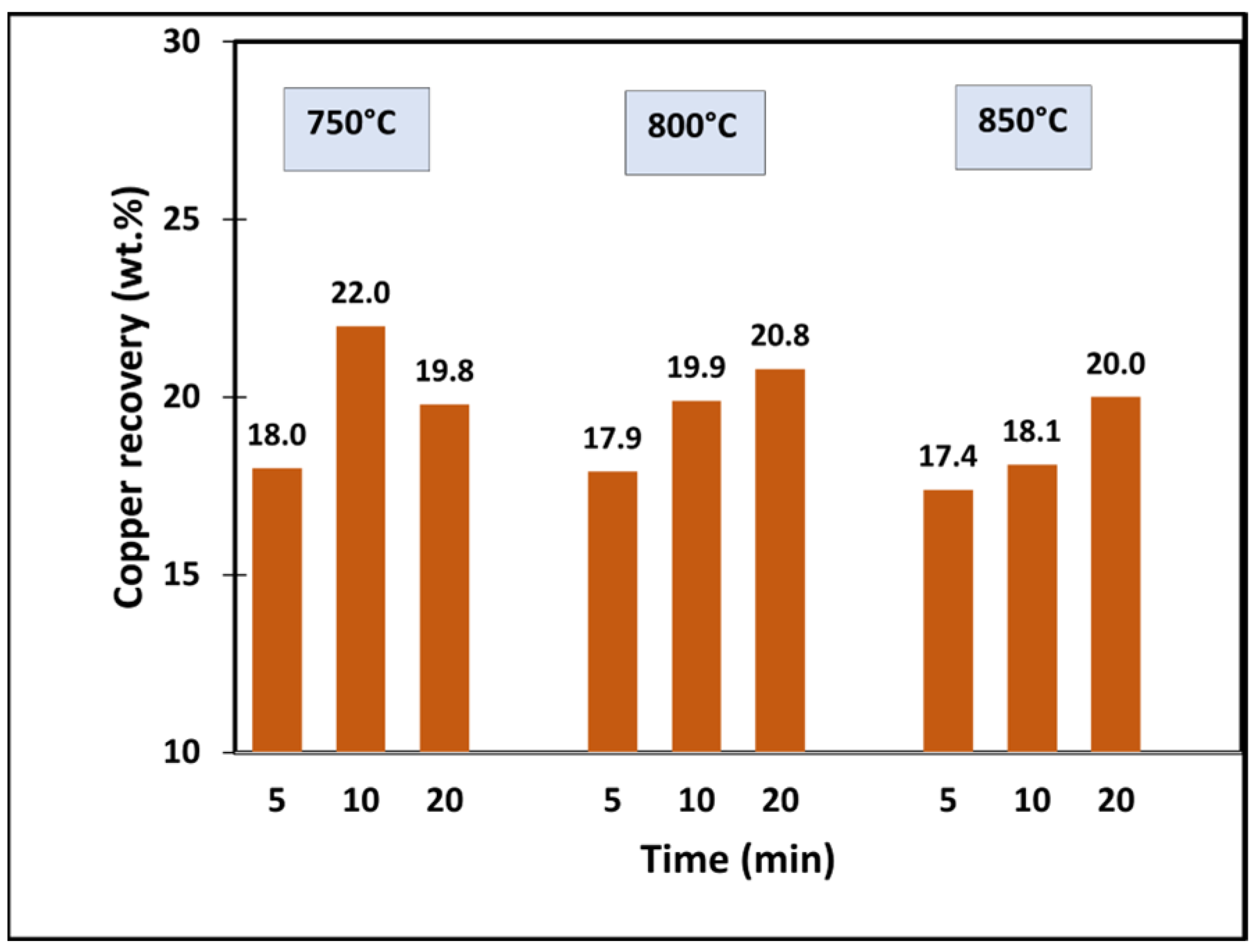
4.3. Extraction of Copper Foils

Figure 6 shows copper foils recovered after the heat treatment of PCBs and their manual separation from the charred residues. It can clearly be seen that copper foils could be extracted with all nine sets of operating conditions that were used as ‘grid-mapping’ for identifying optimal conditions. All electronic components attached to the ‘as-received’ PCBs before the heat treatment, had fallen off the boards. These findings suggest that the prior removal of ECs before heat treatments may not be necessary for the extraction of copper foils from waste PCBs. Figure 7 shows the relative proportion of copper present in waste PCB residues after the heat treatments. These were found to range between 17.4 and 22.0 wt.%. There was no well-defined trend or pattern in the amounts of copper recovered under different operating conditions.

4.4. Characterization of Copper Foils

Copper foils were characterized using a variety of analytical techniques.

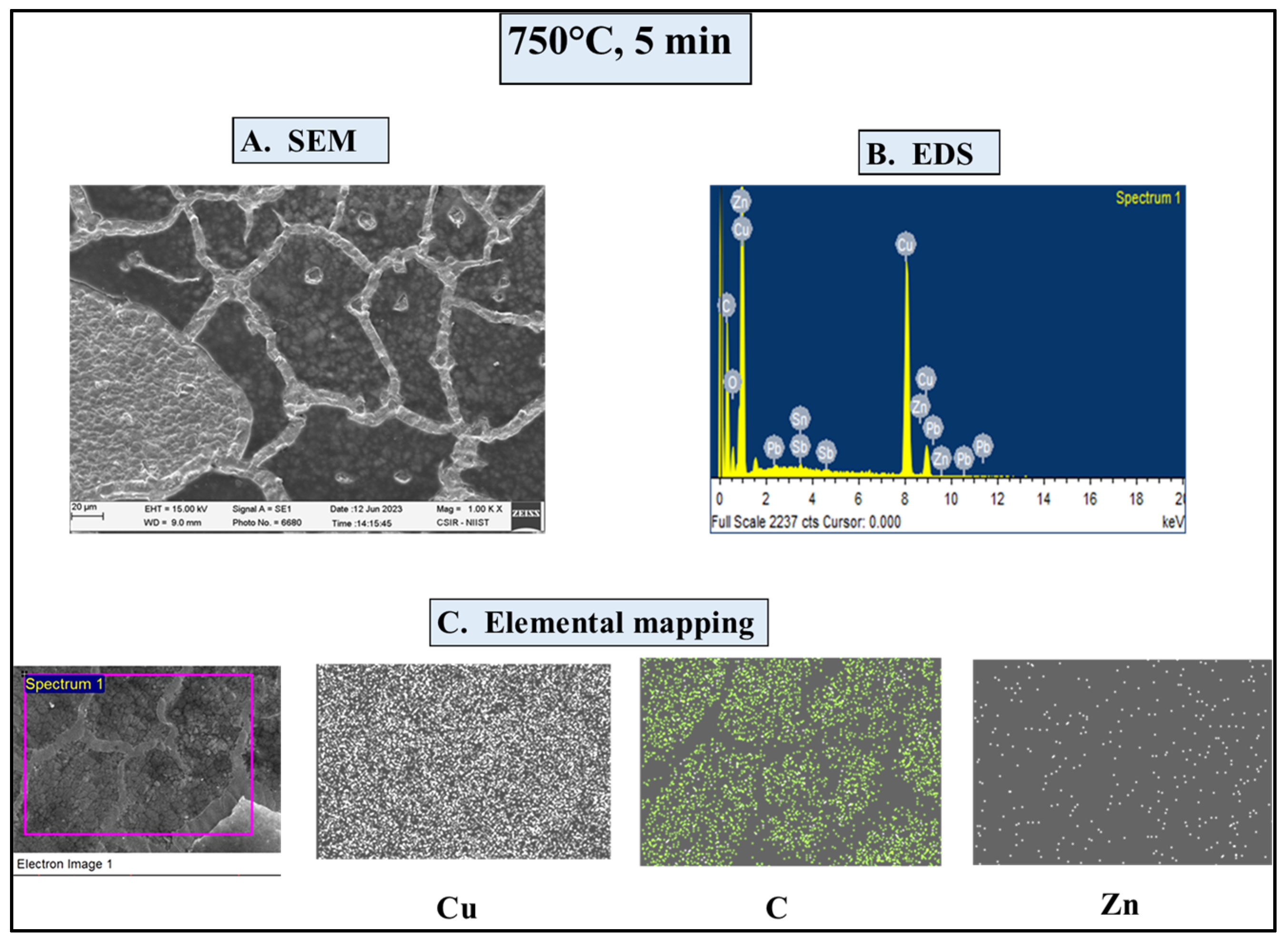
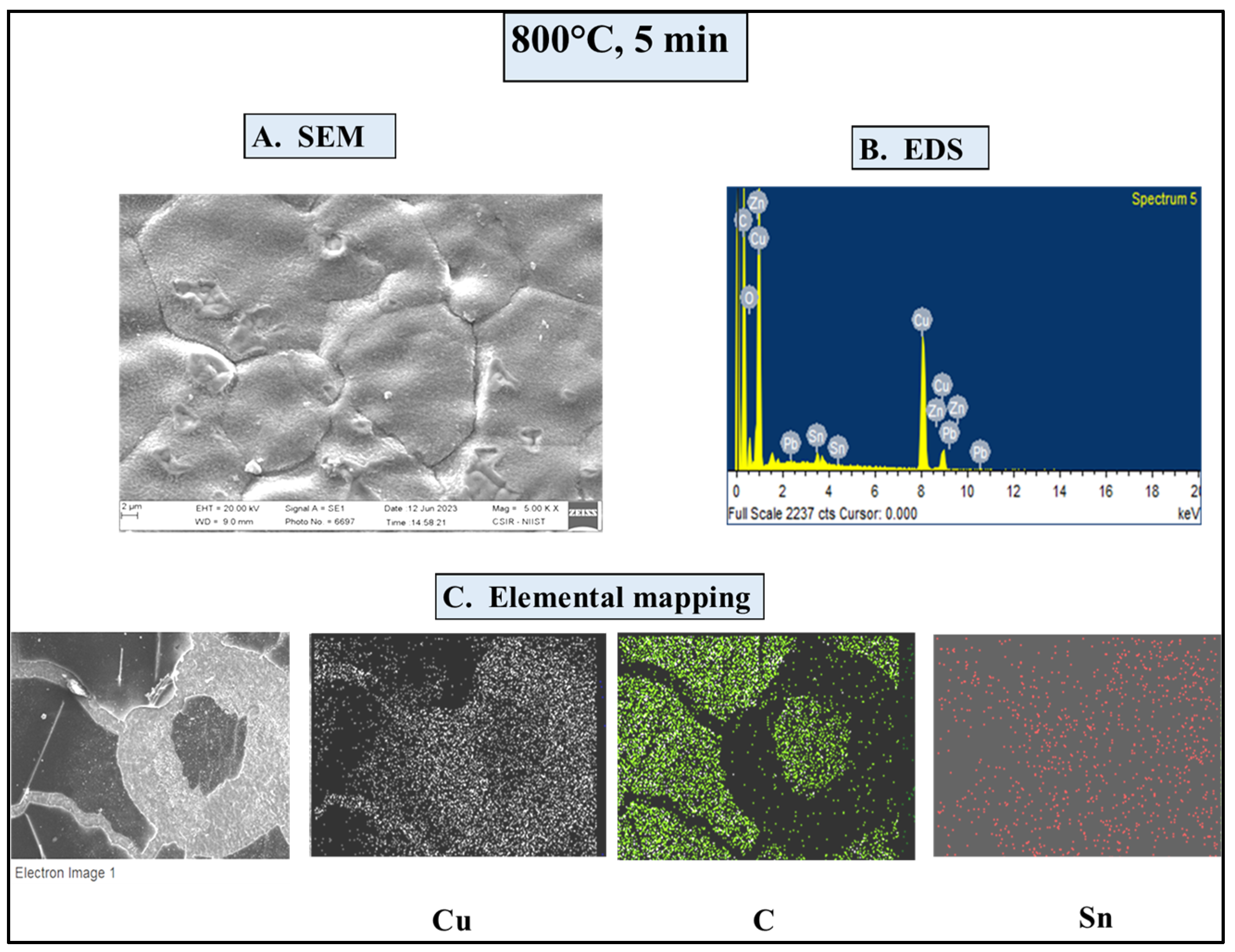
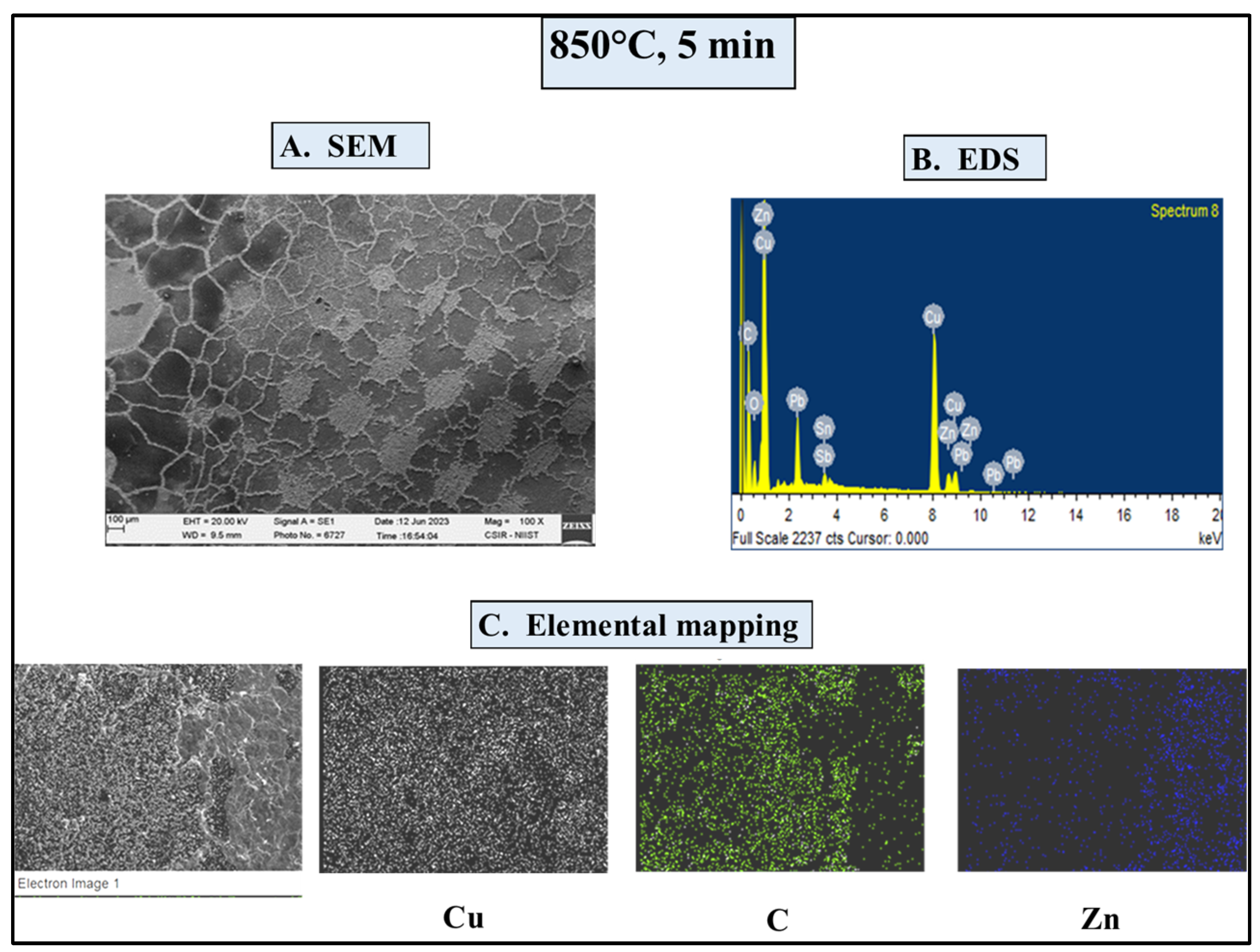
4.4.1. SEM/EDS Investigations

In-depth microscopic investigations were carried out on all sets of copper foils recovered from the heat-treated samples. Detailed SEM/EDS and elemental mapping results are presented for three cases as representative examples. Figure 8 shows SEM/EDS results for a copper foil recovered after heat treatment at 750 °C for 5 min; copper was the main phase present. Trace amounts of metals such as Pb, Sn, Sb, Zn were also identified. There was some evidence for the surface oxidation of the copper foil as well. Small amounts of carbon in the form of chars were also observed atop the copper foil. These chars had formed during polymer degradation, became airborne and finally settled down on the solid residues/copper foils. These chars could be easily scraped off the copper foils and did not present any challenges. The elemental mapping results further support these observations; small amounts of highly volatile Zn were also seen scattered across the foil’s surface.
The SEM/EDS/elemental mapping results for PCBs heat treated at 800 °C and 850 °C for 5 min are shown in Figure 9 and Figure 10, respectively. Apart from differences in their micro-structures, the basic features of the recovered copper foils were unaffected by increases in heat treatment temperatures.

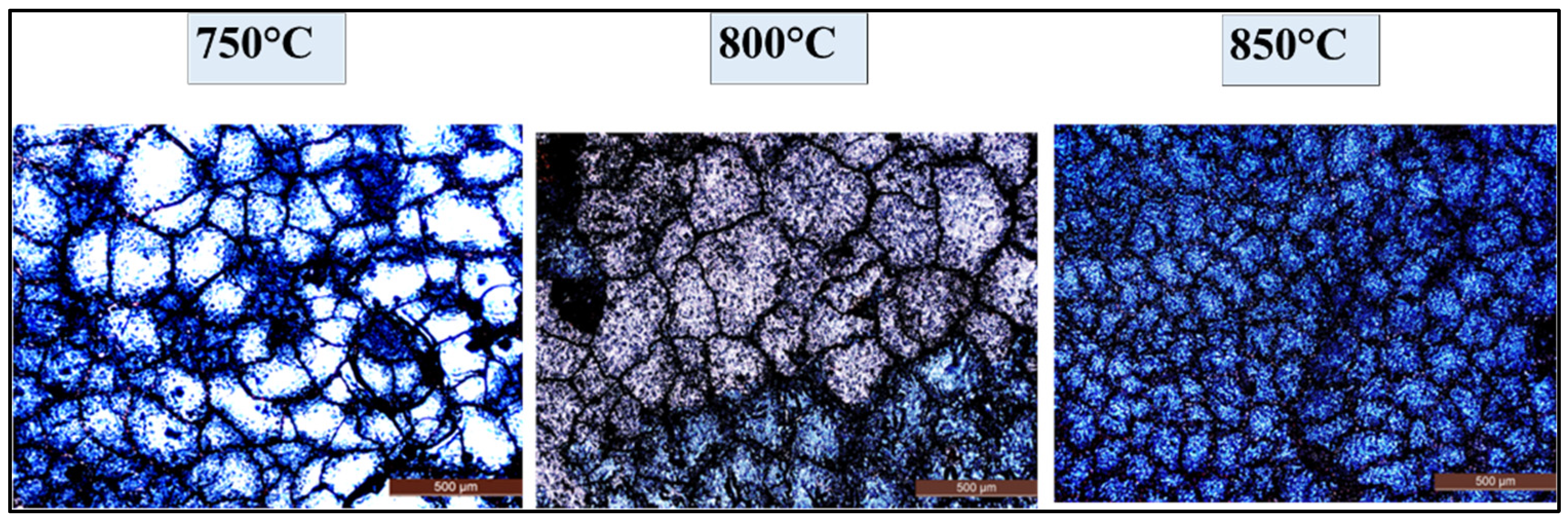
4.4.2. Optical Microscopic Investigations

Optical microscopy results for some representative examples are shown in Figure 11. The blue shade in these figures indicates oxidized copper and the dark shade indicates the deposition of carbon powders. While the microstructure was seen to evolve with increasing temperatures, the results for the three specimens were fundamentally similar. With our primary focus on recovering copper from waste PCBs in this study, the evolution of microstructure was not investigated further.

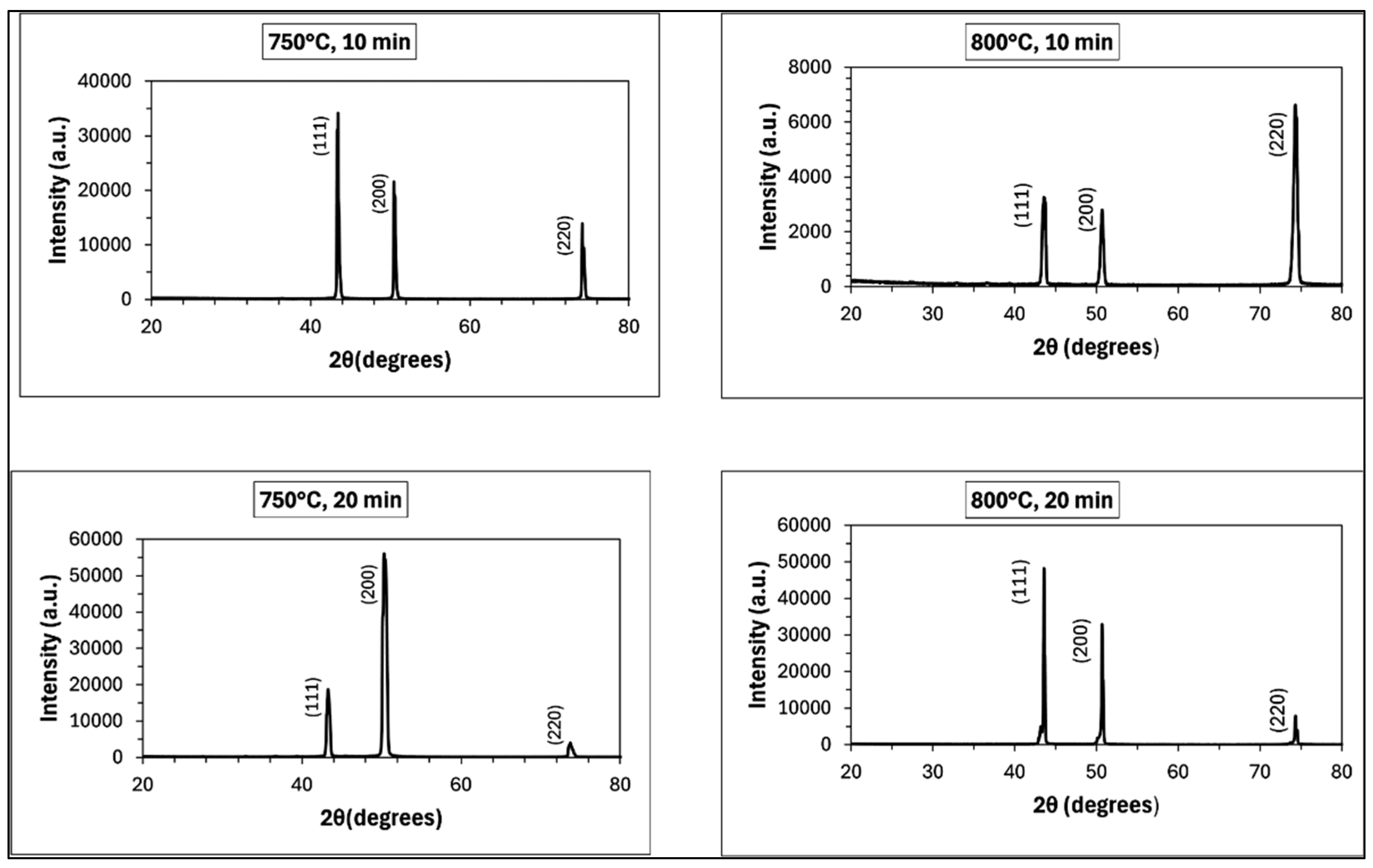
4.4.3. X-ray Diffraction Investigations

XRD investigations were carried out on all the copper foils recovered. A few representative examples are shown in Figure 12. Data are shown for four sets of copper foils: (750 °C, 10 min); (750 °C, 20 min); (800 °C, 10 min); (800 °C, 20 min). Only Cu peaks were observed in all four spectra; no other element such as Pb, Sn or Pb were detected, pointing to their low concentrations. However, a wide variation was observed in the relative peak heights and the total intensity observed for copper peaks. As per the JCPDS (04–0836) data file for Cu, the relative intensities of the (111), (200) and (220) peaks should be 100%, 46% and 20%, respectively. The wide variations in peak heights observed thereby indicate a significant level of preferred orientation in the recovered copper foils.

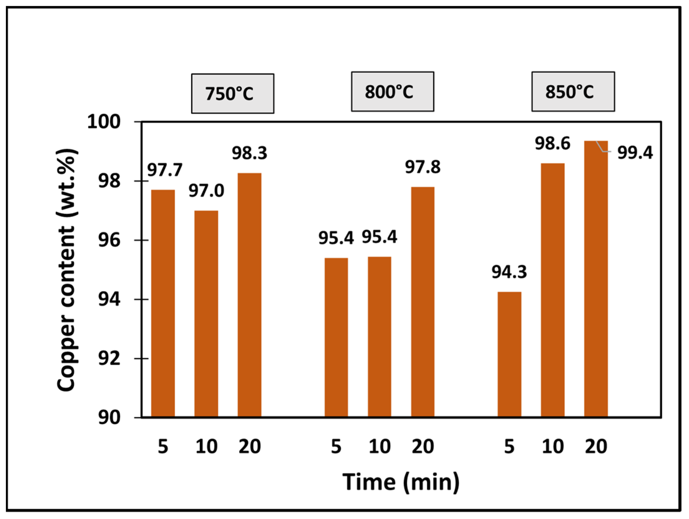
4.4.4. Chemical Composition of Copper Foils

The results presented here are based on the EDS data collected from the entire area of SEM images and are not just limited to specific localized points on the images. Copper, tin, zinc and lead were the key metallic constituents present; the data on non-metals carbon and oxygen were not considered during this analysis. The results for copper are presented in Figure 13; the corresponding proportions of Zn, Pb and Sn impurities are shown in Figure 14. The concentration of copper in the metallic fraction was found to range between 94.3 and 99.4 wt.%. The concentrations of impurities were found to be quite small across the broad spectrum. There was a significant range in the impurity concentrations; no well-defined trends were observed. Generally speaking, the overall purity of the copper foils can be termed as high and determined to be around 95 wt.% or so. Due to the limited accuracy of EDS results (±5%), these studies were supplemented with ICP-MS analysis on copper foils recovered after 5 min of treatment at three temperatures (Table 1). These indicate higher concentrations of Sn with copper concentrations ranging between 85 and 92 wt.%. Based on EDS and ICP data, the overall copper content of the foils was estimated to be 85 wt.% or higher. The XRD data were in good agreement with these findings, indicating low levels of impurities in the foils recovered.

5. Discussion

Detailed results for the recovery of copper foils from waste PCBs have been presented in Figure 3, Figure 4, Figure 5, Figure 6, Figure 7, Figure 8, Figure 9, Figure 10, Figure 11, Figure 12, Figure 13 and Figure 14. High purity copper foils were recovered successfully from waste PCBs with a minimal initial pre-treatment and a single pyrolysis step. An in-depth discussion of these results is provided next.

5.1. Pre-Treatment Steps

To limit local area contamination and associated pollution, current trends in e-waste recycling are favouring the non-removal of electronic components prior to waste PCB processing [46]. Conventional labour-intensive approaches to remove ECs include, among others, acid washing with aqua regia, removing plastics through open burning, electrolysis, separation by coal-heated grill with pliers, etc., resulting in acidulous leachates, local area pollution and harmful emissions [49,50]. In this investigation, mounted ECs had become detached from the PCBs during the pyrolysis step itself (see Figure 4). As low temperature pyrolysis was carried at temperatures higher than typical polymer degradation temperatures, the polymers present in PCBs had completely degraded into gaseous fractions, tars and chars, and were therefore not able to hold the PCB assembly together. This resulted in the breakdown of the PCB ensemble, exfoliation and disintegration of various attachments/connections of various ECs mounted on the board. This result suggests that the prior removal of ECs may not be necessary or an essential requirement for recovering copper foils from waste PCBs. Such removal takes place automatically as part of this new approach.
Size reduction through crushing/milling/powdering is considered to be an essential step for liberating metals from the non-metallic constituents of PCBs [56]. Complete separation of metallic and non-metallic constituents has been reported after milling to ~150 μm sizes [57]; metals were generally found to be concentrated in <1000 μm fractions [58]. These processes are, however, associated with the loss of valuable materials, energy consumption, manual labour, dust generation and local area contamination [61]. The present study provides unambiguous evidence for a sustainable recovery of copper foils without any special separation processes, thereby deeming mechanical pre-treatments are quite avoidable and not necessary at all.

5.2. Exfoliation Technique

The exfoliation technique has found application in a variety of scenarios. For example, Liu et al. [63] have prepared graphite nano-platelets by exfoliating flake graphite using phenolic resin and ball milling for incorporation in low carbon magnesia-carbon refractory bricks. Alzate et al. [64] have extracted non-leaching Au from waste PCBs through exfoliation with (NH4)2S2O8 and oxygen through the oxidative dissolution and breaking of various metallic bonds in the system without using strong acids. Kang et al. [65] have produced copper concentrates through the exfoliation of PCBs using dimethylacetamide. Organic solvents such as DMSO and NMP are also used for delamination for ease of operation, regeneration, low costs, high thermal stability, etc. These organics have limited commercial viability due to their hygroscopic nature, excessive energy consumption and several health-related issues [65]. However, these studies were carried out on blank PCBs without any ECs. It is not apriori certain whether ECs mounted on waste PCBs will also become detached during these processes. In the present case, we have successfully recovered copper foils using the exfoliation route without using chemicals, and without the pre-removal of electronic components.

5.3. Choice of Operational Parameters

The choice of operating temperatures and gaseous atmospheres is also of crucial importance. During the early years of e-waste processing, open burning, low temperature heating, multi-stage processes and mixing of e-waste with other materials were common practises [61]. It was common to heat PCBs in the temperature range 350–600 °C under oxidizing conditions and mixing with ores, etc. [66]. Due to thermal processing in a closed inert environment, pyrolysis of waste PCBs at temperatures above 600 °C is known to prevent the release of persistent organic and brominated pollutants; such contamination can be a serious issue during the incineration or combustion of e-waste [67]. While temperatures below 700 °C are not recommended due to the incomplete destruction of dioxins and furans [68], there can be other issues associated with using too high operating temperatures. Cayumil et al. [20] carried out heat treatments of waste PCBs at 1150 °C in an attempt to recover copper. As this temperature was above the melting point of copper (1084.8 °C), metallic droplets of Cu-Sn-Pb alloys were recovered instead of pure copper. Cayumil et al. [35] were able to recover high purity copper from waste PCBs by heat treatments in the temperature range 800–1000 °C for times between 10 and 60 min; these studies were however carried out crushed PCBs without ECs. In the present study, high purity copper foils were recovered without much difficulty through a judicious choice of operating conditions.

5.4. Copper Recovery

While both hydrometallurgical and bio-metallurgical treatments require a powdered/small sized input for extracting copper from waste PCBs [56], recovered copper is in a crushed state and needs to be separated from other constituents using a variety of techniques [66]. There is no such size requirement in the pyrometallurgical route. Commercial scale recycling of e-waste is being carried out at Rönnskar, Sweden, where up to 14 wt.% e-waste powders are added to copper ore and heated to 1250 °C in air using standard copper processing, followed by subsequent purification [26]. Copper is then recovered indirectly in a multi-stage process in the form of copper matte. High purity copper, present initially in waste PCBs, is first oxidized and then transformed in a number of stages for the final extraction. In the present study, we have successfully recovered copper in a single pyrolysis step without any oxidation, subsequent reduction or requirement for separation from other metallic powders.
A wide variety of techniques and approaches have been developed to recover copper from waste PCBs [25,26,27,28,29,30,31,32,33,34,35,36,37]. It is generally possible to recover most of the copper present (in excess of 80%) using single-stage or multiple-step recovery techniques as detailed in Section 2. In the present investigation, we have bypassed the key processing steps in mechanical pre-treatment and EC removal. However, it had little impact on the quality and quantity of copper recovered, which was either equivalent or better than most cases reported in the literature. This indicates that the present technique can achieve the typical standards of copper recovery in waste PCB recycling.

5.5. Economic Impact and Future Directions

Maximizing resource efficiency and capitalizing on the intrinsic economic values have been the main drivers of e-waste recycling. However, current approaches for resource recovery from waste PCBs generally involve a very large number of processing steps including sorting, removal of electronic components, crushing, grinding, milling, etc. Each of these steps require manpower, machinery, energy, space and infrastructure [69]. All of these processes cost a lot of money, and there can be significant material loss and local area contamination as well. Up to 20% of recycling costs could be associated with these initial processing steps [16]. Bypassing most of the initial pre-treatments, the present study is a significant step forward in enhancing the economic viability of copper recovery from waste PCBs.
The amount of copper recovered during various experiments were found to range between 17.4 wt.% and 22 wt.% (Figure 7). This result indicates that the copper yield from a tonne (1000 kg) of waste PCBs will range between 174 and 220 kg. With current prices of copper scrap being ~ USD 10.5/kg [70], the copper recovery will be worth ~ USD 1827 to USD 2310 per tonne of waste PCBs. In addition to copper, further studies are planned on recovering precious metals gold, silver, platinum, palladium, rare earth elements and other valuable using the current approach. These additional recoveries will significantly enhance the overall profitability of waste PCB recycling.

6. Concluding Remarks

The environmentally sustainable and cost-effective transformation of waste to resources is essential for the future economic growth and long-term material security across the world. As the field of e-waste recycling and material recovery becomes progressively mature, it is important to critically revisit and assess some of the standard procedures. This study has shown that the standard practises of mechanical pre-treatment and the pre-removal of ECs may not be necessary during pyrometallurgical recovery of copper from waste PCBs. This would significantly lower the energy consumption and the environmental footprint of resource recovery and waste management. Further studies are currently underway to develop economic and energy efficient pathways for extracting precious metals as well as rare earths from waste PCBs.

Author Contributions

E.I.A.: Methodology, Investigation, Visualization, Writing—Original Draft, K.J.: Resources, Conceptualization, Supervision, Writing—Original Draft. R.K.: Conceptualization, Methodology, Writing, Review and Editing. J.V.: Investigation, Data Curation, Validation. Y.V.K.: Resources, Formal analysis. P.S.M.: Resources, Supervision, Formal analysis. All authors have read and agreed to the published version of the manuscript.

Funding

This research received no external funding.

Institutional Review Board Statement

Not applicable.

Informed Consent Statement

Not applicable.

Data Availability Statement

Data is available with the authors.

Acknowledgments

E.I.A. gratefully acknowledges the financial support for this project as INSPIRE (JRF) fellowship from the Department of Science and Technology, India. E.I.A., K.J. and J.V. would like to thank The Director of CSIR—National Institute for Interdisciplinary Science and Technology (NIIST), Thiruvananthapuram—for his permission to publish this article. The authors also express their gratitude for the technical support and analytical facilities at NIIST, Thiruvananthapuram, India.

Conflicts of Interest

The authors declare no conflicts of interest.

References

  1. Forecast Number of Mobile Users Worldwide from 2020 to 2025. 2021. Available online: https://www.statista.com/statistics/218984/number-of-global-mobile-users-since-2010/ (accessed on 6 June 2024).
  2. Forecast Number of Mobile Devices Worldwide from 2020 to 2025 (in Billions). 2021. Available online: https://www.statista.com/statistics/245501/multiple-mobile-device-ownership-worldwide/ (accessed on 7 June 2024).
  3. Tansel, B. From Electronic Consumer Products to E-Wastes: Global Outlook, Waste Quantities, Recycling Challenges. Environ. Int. 2017, 98, 35–45. [Google Scholar] [CrossRef] [PubMed]
  4. Forti, V.; Baldé, C.P.; Kuehr, R.; Bel, G. The Global E-Waste Monitor 2020: Quantities, Flows, and the Circular Economy Potential; United Nations University: Bonn, Germany, 2020. [Google Scholar]
  5. Baldé, C.P.; van den, B.S.; Forti, V.; van der, S.A.; Hopstaken, F. The Dutch WEEE Flows 2020: What Happened between 2010 and 2018; United Nations University (UNU)/United Nations Institute for Training and Research (UNITAR): Tokyo, Japan, 2020. [Google Scholar]
  6. Van Yken, J.; Boxall, N.J.; Cheng, K.Y.; Nikoloski, A.N.; Moheimani, N.R.; Kaksonen, A.H. E-Waste Recycling and Resource Recovery: A Review on Technologies, Barriers and Enablers with a Focus on Oceania. Metals 2021, 11, 1313. [Google Scholar] [CrossRef]
  7. Duran, J.A.G.; Arroyo, Z.G.; Gómez Castro, F.I.; Owen, P.Q.; Cadena, L.E.S.; Gómez, M.V.A. Evaluation of the effect of physical and chemical factors in the recovery of Cu, Pb and Fe from waste PCB through acid leaching. Heliyon 2023, 9, e21348. [Google Scholar] [CrossRef] [PubMed]
  8. Segura-Bail’, B.; Lapidus, G.T. Selective recovery of copper contained in waste PCBs from cell phones with impurity inhibition in the citrate-phosphate system. Hydrometallurgy 2021, 203, 105699. [Google Scholar] [CrossRef]
  9. Nagarajan, N.; Panchatcharam, P. Cost-Effective and Eco-Friendly Copper Recovery from Waste Printed Circuit Boards Using Organic Chemical Leaching. Heliyon 2023, 9, e13806. [Google Scholar] [CrossRef] [PubMed]
  10. Esyra, K.; Ishak, H.K.; Ismail, S.; Irfan, M.; Razak, B.A. Recovery of copper and valuable metals from E-waste via hydrometallurgical method. J. Mater. Today 2022, 66, 3077–3081. [Google Scholar]
  11. Faraji, F.; Golmohammadzadeh, R.; Pickles, C.A. Potential and current practices of recycling waste printed circuit boards: A review of the recent progress in pyrometallurgy. J. Environ. Manag. 2022, 316, 115242. [Google Scholar] [CrossRef] [PubMed]
  12. Kim, Y.M.; Kim, S.; Lee, J.Y.; Park, Y.K. Pyrolysis Reaction Pathways of Waste Epoxy-Printed Circuit Board. Environ. Eng. Sci. 2013, 30, 706–712. [Google Scholar] [CrossRef]
  13. Chen, W.; Shu, Y.; Li, Y.; Chen, Y.; Wei, J. Co-Pyrolysis of Waste Printed Circuit Boards with Iron Compounds for Br-Fixing and Material Recovery. Environ. Sci. Pollut. Res. 2021, 28, 64642–64651. [Google Scholar] [CrossRef]
  14. Guo, J.; Guo, J.; Xu, Z. Recycling of Non-Metallic Fractions from Waste Printed Circuit Boards: A Review. J. Hazard. Mater. 2009, 168, 567–590. [Google Scholar] [CrossRef]
  15. Rajagopal, R.R.; Aravinda, L.S.; Rajarao, R.; Bhat, B.R.; Sahajwalla, V. Activated Carbon Derived from Non-Metallic Printed Circuit Board Waste for Supercapacitor Application. Electrochim. Acta 2016, 211, 488–498. [Google Scholar] [CrossRef]
  16. Manikandan, S.; Inbakandan, D.; Valli Nachiyar, C.; Karthick Raja Namasivayam, S. Towards Sustainable Metal Recovery from E-Waste: A Mini Review. Sustain. Chem. Environ. 2023, 2, 100001. [Google Scholar] [CrossRef]
  17. Islam, A.; Ahmed, T.; Awual, M.R.; Rahman, A.; Sultana, M.; Aziz, A.A.; Monir, M.U.; Teo, S.H.; Hasan, M. Advances in Sustainable Approaches to Recover Metals from E-Waste-A Review. J. Clean. Prod. 2020, 244, 118815. [Google Scholar] [CrossRef]
  18. Williams, P.T. Valorization of Printed Circuit Boards from Waste Electrical and Electronic Equipment by Pyrolysis. Waste Biomass Valoriz. 2010, 1, 107–120. [Google Scholar] [CrossRef]
  19. Huang, Y.F.; Chou, S.L.; Lo, S.L. Gold Recovery from Waste Printed Circuit Boards of Mobile Phones by Using Microwave Pyrolysis and Hydrometallurgical Methods. Sustain. Environ. Res. 2022, 32, 6. [Google Scholar] [CrossRef]
  20. Cayumil, R.; Khanna, R.; Ikram-Ul-Haq, M.; Rajarao, R.; Hill, A.; Sahajwalla, V. Generation of Copper Rich Metallic Phases from Waste Printed Circuit Boards. Waste Manag. 2014, 34, 1783–1792. [Google Scholar] [CrossRef] [PubMed]
  21. Lennartsson, A.; Engström, F.; Samuelsson, C.; Björkman, B.; Pettersson, J. Large-Scale WEEE Recycling Integrated in an Ore-Based Cu-Extraction System. J. Sustain. Metall. 2018, 4, 222–232. [Google Scholar] [CrossRef]
  22. Khanna, R. Global Perspectives on Regulatory Measures and Collection Procedures for Electronic Waste: A Critical Assessment. Open Access J. Waste Manag. Xenobiot. 2018, 1, 000101. [Google Scholar] [CrossRef]
  23. Kiddee, P.; Naidu, R.; Wong, M.H. Electronic Waste Management Approaches: An Overview. Waste Manag. 2013, 33, 1237–1250. [Google Scholar] [CrossRef]
  24. Sthiannopkao, S.; Wong, M.H. Handling E-Waste in Developed and Developing Countries: Initiatives, Practices, and Consequences. Sci. Total Environ. 2013, 463–464, 1147–1153. [Google Scholar] [CrossRef]
  25. Choubey, P.K.; Panda, R.; Jha, M.K.; Lee, J.C.; Pathak, D.D. Recovery of Copper and Recycling of Acid from the Leach Liquor of Discarded Printed Circuit Boards (PCBs). Sep. Purif. Technol. 2015, 156, 269–275. [Google Scholar] [CrossRef]
  26. Cayumil, R. Recycling of Electronic Waste for the Recovery of Value-Added Materials. Ph.D. Thesis, University of New South Wales, Sydney, Australia, 2016. [Google Scholar]
  27. Patel, A.; Kumar, S.; Awasthi, A. Hydrometallurgy: Urban mining of E-waste and its future implications. In Global E-Waste Management Strategies and Future Implications; Arya, S., Kumar, S., Eds.; Elsevier: Amsterdam, The Netherlands, 2023; Volume 6, pp. 105–123. ISBN 9780323999199. [Google Scholar] [CrossRef]
  28. Xua, Y.; Lia, J.; Liu, L. Current status and future perspective of recycling copper by hydrometallurgy from waste printed circuit boards. Procedia Environ. Sci. 2016, 31, 162–170. [Google Scholar] [CrossRef]
  29. Wu, W.; Liu, X.; Xu Zhang, X.; Zhu, M.; Tan, W. Bioleaching of copper from waste printed circuit boards by bacteria-free cultural supernatant of iron–sulfur-oxidizing bacteria. Bioresour. Bioprocess. 2018, 5, 10. [Google Scholar] [CrossRef]
  30. Adhapure, N.N.; Dhakephalkar, P.K.; Dhakephalkar, A.P.; Tembhurkar, V.R.; Rajgure, A.V.; Deshmukh, A.M. Use of large pieces of printed circuit boards for bioleaching to avoid ‘precipitate contamination problem’ and to simplify overall metal recovery. MethodX 2014, 1, e181–e186. [Google Scholar] [CrossRef] [PubMed]
  31. Jujun, R.; Jie, Z.; Jian, H.; Zhang, J. A Novel Designed Bioreactor for Recovering Precious Metals from Waste Printed Circuit Boards. Sci. Rep. 2015, 5, 13481. [Google Scholar] [CrossRef] [PubMed]
  32. Long, L.; Sun, S.; Zhong, S.; Dai, W.; Liu, J.; Song, W. Using vacuum pyrolysis and mechanical processing for recycling waste printed circuit boards. J. Hazard. Mater. 2019, 177, 626–632. [Google Scholar] [CrossRef] [PubMed]
  33. Zhou, G.; Luo, Z.; Zhai, X. Experimental study on metal recycling from waste PCB. In Proceedings of the International Conference on Sustainable Solid Waste Management 2007, Chennai, India, 5–7 September 2007; pp. 155–162. [Google Scholar]
  34. Zhan, L.; Xu, Z. Separating and Recycling Metals from Mixed Metallic Particles of Crushed Electronic Wastes by Vacuum Metallurgy. Environ. Sci. Technol. 2009, 43, 7074–7078. [Google Scholar] [CrossRef] [PubMed]
  35. Cayumil, R.; Ikram-Ul-Haq, M.; Khanna, R.; Saini, R.; Mukherjee, P.S.; Mishra, B.K.; Sahajwalla, V. High Temperature Investigations on Optimising the Recovery of Copper from Waste Printed Circuit Boards. Waste Manag. 2018, 73, 556–565. [Google Scholar] [CrossRef] [PubMed]
  36. Xiu, F.R.; Zhang, F.S. Recovery of Copper and Lead from Waste Printed Circuit Boards by Supercritical Water Oxidation Combined with Electrokinetic Process. J. Hazard. Mater. 2009, 165, 1002–1007. [Google Scholar] [CrossRef]
  37. Silvas, F.P.C.; Jiménez Correa, M.M.; Caldas, M.P.K.; de Moraes, V.T.; Espinosa, D.C.R.; Tenório, J.A.S. Printed Circuit Board Recycling: Physical Processing and Copper Extraction by Selective Leaching. Waste Manag. 2015, 46, 503–510. [Google Scholar] [CrossRef]
  38. Fogarasi, S.; Imre-Lucaci, F.; Imre-Lucaci, Á.; Ilea, P. Copper Recovery and Gold Enrichment from Waste Printed Circuit Boards by Mediated Electrochemical Oxidation. J. Hazard. Mater. 2014, 273, 215–221. [Google Scholar] [CrossRef]
  39. Cayumil, R.; Khanna, R.; Rajarao, R.; Ikram-ul-Haq, M.; Mukherjee, P.S.; Sahajwalla, V. Environmental Impact of Processing Electronic Waste—Key Issues and Challenges. In E-Waste in Transition—From Pollution to Resource; InTech: London, UK, 2016. [Google Scholar]
  40. Mckay, G. Dioxin Characterisation, Formation and Minimisation during Municipal Solid Waste (MSW) Incineration: Review. Chem. Eng. J. 2002, 86, 343–368. [Google Scholar] [CrossRef]
  41. Wang, Y.; Xu, C.; Yu, X.; Zhang, H.; Han, M. Multilayer flexible electronics: Manufacturing approaches and applications. Mater. Today Physics. 2022, 23, 100647. [Google Scholar] [CrossRef]
  42. Cucchiella, F.; D’Adamo, I.; Lenny Koh, S.C.; Rosa, P. Recycling of WEEEs: An Economic Assessment of Present and Future E-Waste Streams. Renew. Sustain. Energy Rev. 2015, 51, 263–272. [Google Scholar] [CrossRef]
  43. Daware, S.; Chandel, S.; Rai, B. A Machine Learning Framework for Urban Mining: A Case Study on Recovery of Copper from Printed Circuit Boards. Miner. Eng. 2022, 180, 107479. [Google Scholar] [CrossRef]
  44. Mesquita, R.A.; Silva, R.A.F.; Majuste, D. Chemical Mapping and Analysis of Electronic Components from Waste PCB with Focus on Metal Recovery. Process Saf. Environ. Prot. 2018, 120, 107–117. [Google Scholar] [CrossRef]
  45. Kaya, M. Recovery of Metals and Nonmetals from Electronic Waste by Physical and Chemical Recycling Processes. Waste Manag. 2016, 57, 64–90. [Google Scholar] [CrossRef] [PubMed]
  46. Khanna, R.; Mukherjee, P.S.; Park, M. A Critical Assessment on Resource Recovery from Electronic Waste: Impact of Mechanical Pre-Treatment. J. Clean. Prod. 2020, 268, 122319. [Google Scholar] [CrossRef]
  47. Wang, J.; Xu, Z. Disposing and Recycling Waste Printed Circuit Boards: Disconnecting, Resource Recovery, and Pollution Control. Environ. Sci. Technol. 2015, 49, 721–733. [Google Scholar] [CrossRef]
  48. Wang, H.; Zhang, S.; Li, B.; Pan, D.; Wu, Y.; Zuo, T. Recovery of Waste Printed Circuit Boards through Pyrometallurgical Processing: A Review. Resour. Conserv. Recycl. 2017, 126, 209–218. [Google Scholar] [CrossRef]
  49. Wang, J.; Guo, J.; Xu, Z. An Environmentally Friendly Technology of Disassembling Electronic Components from Waste Printed Circuit Boards. Waste Manag. 2016, 53, 218–224. [Google Scholar] [CrossRef] [PubMed]
  50. Maurice, A.A.; Dinh, K.N.; Charpentier, N.M.; Brambilla, A.; Gabriel, J.C.P. Dismantling of Printed Circuit Boards Enabling Electronic Components Sorting and Their Subsequent Treatment Open Improved Elemental Sustainability Opportunities. Sustainability 2021, 13, 10357. [Google Scholar] [CrossRef]
  51. Zhang, D.; Dong, L.; Li, Y.T.; Wu, Y.; Ma, Y.X.; Yang, B. Copper Leaching from Waste Printed Circuit Boards Using Typical Acidic Ionic Liquids Recovery of E-Wastes’ Surplus Value. Waste Manag. 2018, 78, 191–197. [Google Scholar] [CrossRef] [PubMed]
  52. Martino, R.; Iseli, C.; Gaydardzhiev, S.; Streicher-Porte, M.; Weh, A. Electro Dynamic Fragmentation of Printed Wiring Boards as a Preparation Tool for Their Recycling. Miner. Eng. 2017, 107, 20–26. [Google Scholar] [CrossRef]
  53. Veit, H.M.; Pereira, C.C.; Hörlle, L.F.; Bernardes, A.M. Recycling of metals from PCB by dense medium separation process. In Recycling and Waste Treatment in Mineral and Metal Processing: Technical and Economic Aspects; June: Luleå, Sweden, 2002; pp. 16–20. [Google Scholar]
  54. Zhang, S.; Forssberg, E. Mechanical Separation-Oriented Characterization of Electronic Scrap. Resour. Conserv. Recycl. 1997, 21, 247–269. [Google Scholar] [CrossRef]
  55. Kaya, M. Recovery of Metals from Electronic Waste by Physical and Chemical Recycling Processes. Int. Sch. Sci. Res. Innov. 2016, 10, 259–270. [Google Scholar] [CrossRef]
  56. Kaya, M. Electronic Waste and Printed Circuit Board Recycling Technologies; Springer International Publishing: Cham, Switzerland, 2019; ISBN 978-3-030-26592-2. [Google Scholar] [CrossRef]
  57. Sander, S.; Schubert, G.; Jäckel, H.G. The Fundamentals of the Comminution of Metals in Shredders of the Swing-Hammer Type. Int. J. Miner. Process. 2004, 74, S385–S393. [Google Scholar] [CrossRef]
  58. Tiwary, C.S.; Kishore, S.; Vasireddi, R.; Mahapatra, D.R.; Ajayan, P.M.; Chattopadhyay, K. Electronic Waste Recycling via Cryo-Milling and Nanoparticle Beneficiation. Mater. Today 2017, 20, 67–73. [Google Scholar] [CrossRef]
  59. Yang, M.; Liu, H.; Ye, B.; Qian, W. Recycling of Printed Circuit Boards by Abrasive Waterjet Cutting. Process Saf. Environ. Prot. 2021, 148, 805–812. [Google Scholar] [CrossRef]
  60. Xue, M.; Yang, Y.; Ruan, J.; Xu, Z. Assessment of Noise and Heavy Metals (Cr, Cu, Cd, Pb) in the Ambience of the Production Line for Recycling Waste Printed Circuit Boards. Environ. Sci. Technol. 2012, 46, 494–499. [Google Scholar] [CrossRef]
  61. Saini, R.; Khanna, R.; Dutta, R.K.; Cayumil, R.; Ikram-Ul-Haq, M.; Agarwala, V.; Ellamparuthy, G.; Jayasankar, K.; Mukherjee, P.S.; Sahajwalla, V. A Novel Approach for Reducing Toxic Emissions during High Temperature Processing of Electronic Waste. Waste Manag. 2017, 64, 182–189. [Google Scholar] [CrossRef] [PubMed]
  62. Saini, R. Novel Approaches for Processing Waste Printed Circuit Boards. Ph.D. Thesis, Indian Institute of Technology, Roorkee, India, 2018. [Google Scholar]
  63. Liu, M.; Huang, J.; Meng, H.; Liu, C.; Chen, Z.; Yang, H.; Feng, Z.; Li, X.; Luo, R.; Huang, Z.; et al. A novel approach to prepare graphite nanoplatelets exfoliated by three-roll milling in phenolic resin for low-carbon MgO-C refractories. J. Eur. Ceram. Soc. 2023, 43, 4198–4208. [Google Scholar] [CrossRef]
  64. Alzate, A.; López, M.E.; Serna, C. Recovery of gold from waste electrical and electronic equipment (WEEE) using ammonium persulfate. Waste Manag. 2016, 57, 113–120. [Google Scholar] [CrossRef] [PubMed]
  65. Kang, K.D.; Ilankoon, I.M.S.K.; Chong, M.N.; Wu, T.Y. Exfoliation of coarse printed circuit boards using dimethylacetamide: Production of copper concentrates. Miner. Eng. 2023, 191, 107963. [Google Scholar] [CrossRef]
  66. Cui, J.; Zhang, L. Metallurgical recovery of metals from electronic waste: A review. J. Hazard. Mater. 2008, 158, 228–256. [Google Scholar] [CrossRef] [PubMed]
  67. Veldhuizen, H.; Sippel, B. Mining discarded electronics. UNEP Ind. Environ. 1994, 17, 7–11. [Google Scholar]
  68. Zhan, Z.; Qiu, K. Pyrolysis kinetics and tg-ftir analysis of waste epoxy printed circuit boards. J. Cent. S. Univ. 2011, 18, 331–336. [Google Scholar] [CrossRef]
  69. Mairizal, A.Q.; Sembada, A.Y.; Tse, K.M.; Haque, N.; Rhamdhani, M.A. Techno-economic analysis of waste PCB recycling in Australia. Resour. Conserv. Recycl. 2023, 190, 106784. [Google Scholar] [CrossRef]
  70. Copper Price (USD/Kilogram) Chart for the Last 10 Years. Available online: https://www.dailymetalprice.com/metalpricecharts.php?c=cu&u=kg&d=24 (accessed on 12 July 2024).
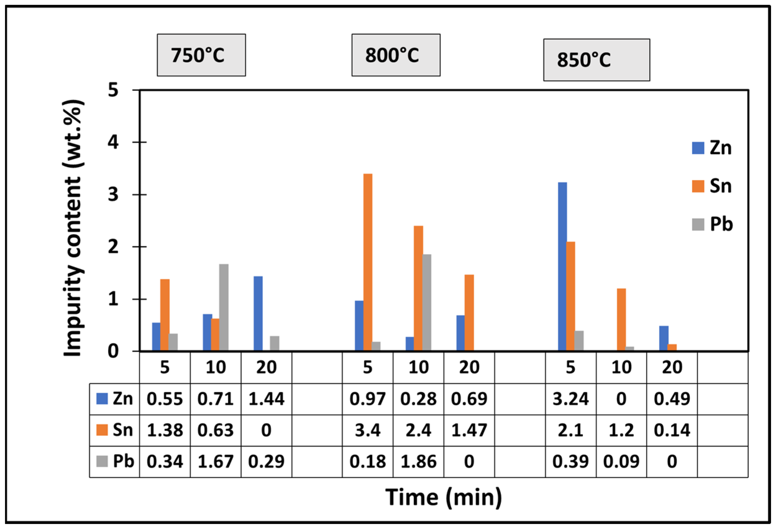
Figure 1. (A) Schematic representation of a typical PCB. (B) A variety of electronic components mounted on a power supply PCB. (C) E-waste as a collection of PCBs in a range of sizes, shapes and component configurations.
Sustainability 16 06269 g001
Figure 2. (A) A schematic representation of the furnace and the experimental arrangement. (B) Inconel crucible loaded with several pieces cut from ‘as-received’ PCBs.
Sustainability 16 06269 g002
Figure 3. A collection of as received PCBs: (A) before, and (B) after the heat treatment.
Sustainability 16 06269 g003
Figure 4. Copper foils and other residuals recovered from the heat-treated PCBs. Copper foils cleaned with ethanol sonification are also shown in the figure.
Sustainability 16 06269 g004
Figure 5. Estimated loss of polymers during low temperature pyrolysis of waste PCBs.
Sustainability 16 06269 g005
Figure 6. Copper foils recovered after various heat treatments at temperatures (750–850 °C) and for times between 5 and 20 min.
Sustainability 16 06269 g006
Figure 7. Recovery of copper after heat treatments at a range of temperatures and heating times.
Sustainability 16 06269 g007
Figure 8. The SEM/EDS results on copper foils recovered after heat treatment at 750 °C for 5 min along with elemental mapping results.
Sustainability 16 06269 g008
Figure 9. The SEM/EDS results on copper foils recovered after heat treatment at 800 °C for 5 min along with elemental mapping results.
Sustainability 16 06269 g009
Figure 10. The SEM/EDS results on copper foils recovered after heat treatment at 850 °C for 5 min along with elemental mapping results.
Sustainability 16 06269 g010
Figure 11. Optical microscopy results on the copper foils recovered after various heat treatments for 10 min.
Sustainability 16 06269 g011
Figure 12. X-ray diffraction results on copper foils recovered after various heat treatments.
Sustainability 16 06269 g012
Figure 13. Copper content in the recovered copper foils as determined from the EDS data.
Sustainability 16 06269 g013
Figure 14. Impurity content (wt.%) in the recovered copper foils as determined from EDS data.
Sustainability 16 06269 g014
Table 1. ICP-MS data (wt.%) on copper foils recovered after various heat treatments.
Temperature, TimeSnZnSbCuPb
750 °C, 5 min14.630.030.0485.30<0.01
800 °C, 5 min11.500.190.2788.04<0.01
850 °C, 5 min7.050.680.0292.24<0.01
Disclaimer/Publisher’s Note: The statements, opinions and data contained in all publications are solely those of the individual author(s) and contributor(s) and not of MDPI and/or the editor(s). MDPI and/or the editor(s) disclaim responsibility for any injury to people or property resulting from any ideas, methods, instructions or products referred to in the content.

