Abstract
With the development of millimeter-wave radar systems, substrate-integrated waveguide (SIW) slot antennas have been widely used. This paper presents a computational approach for calculating the equivalent normalized admittance of slot in low sidelobe SIW longitudinal slot antennas. In contrast to the existing methods, this method takes into account the impact of the N-slots coupling on the admittance. Through this method, fitting functions for resonant length and conductance are obtained, which describe the relationship between the resonant length, resonant conductance, and offset of slots. Moreover, based on the two fitting functions, a low sidelobe SIW longitudinal slot linear antenna is designed for millimeter-wave radar applications at 77 GHz. This antenna consists of a transition from the standard WR-12 waveguide to the SIW and a set of radiating slots. The simulation results indicate an impedance bandwidth of 4.8% and a gain of 13.2 dBi. The sidelobe level in the H-plane is below −28 dB, which meets the desired specifications and confirms the accuracy of the presented method.
1. Introduction
The substrate-integrated waveguide (SIW) is a planar microwave transmission technology that has been developed over the past two decades. In 1998, the concepts of “Post-wall Waveguide” and “Laminated Waveguide” were proposed, and they served as the prototype of SIW [1,2]. Furthermore, the concept of an SIW transmission line was formally introduced in 2001 in order to solve the problem of waveguide and plane circuit integration [3]. Eventually, in 2005, the guide wave and leakage characteristics of SIW were studied for the first time, which marked the perfection of the basic theoretical framework of SIW [4]. In the past few years, with the development of millimeter-wave circuit systems, the potential application value of SIW has been well explored due to its inherent advantages [5,6]. In contrast to microstrip lines that have been commonly used in recent years, the use of SIW results in lower transmission losses and a higher power capacity. Moreover, SIW is extensively utilized in vehicle-mounted radar systems due to its ease of processing and seamless integration with other planar circuits.
SIW antennas, developed on the basis of SIW, inherit all the advantages of SIW transmission lines. Moreover, in contrast to microstrip antennas, SIW antennas exhibit reduced susceptibility to surface waves at millimeter-wave frequencies, making them extremely promising for applications in millimeter-wave radar systems [7,8]. As a result, considerable research efforts have been focused on the design of SIW antennas and related circuits. In [9], a “post wall” slot antenna was proposed, which started the upsurge in SIW antenna research. Since then, various types of SIW antennas have been developed, including linear SIW slot arrays [10,11], high-gain SIW resonant cavity antennas [12,13], smaller half-mode SIW (HFSIW) antennas [14], and so forth. To meet the integration demands of SIW antennas and other planar circuits, transition structures from SIW to the microstrip line have been extensively investigated. Among these, the tapered microstrip line structure emerges as a prevalent approach [15,16]. This particular transition offers exceptional impedance matching between the microstrip and the SIW, utilizing a straightforward design. Furthermore, some more efficient transition structures have also been proposed, such as a multilayer substrate structure [17], and a tapered structure on SIW via holes [18]. In recent years, some 3D vertical transitions have garnered significant attention [19,20]. On the other hand, due to the inefficiency of the coaxial line at millimeter-wave frequencies, the standard rectangular waveguide (RWG) is used as the measurement feed interface. Thus, transition structures from RWG to SIW have been investigated extensively. Up to now, transition structures from SIW to standard RWG have been divided into two categories. The first is vertically connected structures, including some innovative patch-loaded coupling cavity configurations [21,22] and multilayer transition architecture [23]. The second category is horizontally connected structures such as a fin-line structure [24] and a height or width stepped waveguide transformer [25,26]. Most studies aim at achieving ultra-wideband and low insertion loss.
In radar systems, high gain and low sidelobe characteristics of antennas are important requirements in order to obtain a longer detection range and prevent spurious object interference. In recent years, significant focus has been directed toward the development of low sidelobe SIW antenna. Many non-uniform feed networks have been designed for the purpose of achieving low sidelobe, low cross-polarization, and high gain in antenna arrays [27,28,29,30]. These arrays are compact, offer high gain, and are predominantly suitable for radar imaging systems. In [31], a broadband patch antenna fed by half-mode substrate-integrated waveguide (HMSIW) is introduced, which achieves both a low sidelobe and high gain. Ref. [32] explores the use of the evanescent mode of a cutoff waveguide for low sidelobe realization, presenting potential applications in wireless communication. However, these antennas and arrays are complex in design, limiting their application in vehicle-mounted MIMO radar. Conversely, SIW longitudinal slot linear antennas are the preferred choice for vehicle millimeter-wave radar systems because they seamlessly integrate with flat-panel circuitry and inherently achieve low sidelobes and high gain.
Therefore, the linear SIW longitudinal slot antenna array has become the preferred choice for automotive radar among various SIW antennas. In the design of low sidelobe SIW longitudinal slot antennas, the method of calculating the slot equivalent conductance plays a crucial role. In the early stage of SIW slot antenna development, the equivalent conductance of the slot was mainly calculated by Stevenson’s equation [33,34,35]. This equation assumes that the length of the slot is half a waveguide wavelength, and the equivalent conductance is a function of the slot offset [36]. However, since the height of the SIW drops sharply, the impact of the slot length on the equivalent conductance cannot be neglected. Subsequently, a method of extracting equivalent admittance based on full-wave simulation software is proposed [37]. This method can measure the equivalent admittance of a signal slot, and similar methods are applied in [38,39]. This type of approach is widely used in the design of SIW antennas; however, they do not take into account the impact of the slot coupling on the conductance in the array. Moreover, the method in [40] can measure the conductance with the slot coupling. This method has been widely applied to the rectangular waveguide slot antenna design and can be applied to the SIW slot antenna design as well. However, susceptance data ares not available in this method. In [41], the periodic boundary condition is used in full-wave simulation software to calculate conductance affected by the slot coupling, but the calculation equation is not provided. In addition to the aforementioned techniques, several innovative methods have been proposed in recent years. In [42], a method to assign amplitude distribution of the slot by changing the SIW width is proposed. This method reduces the design complexity but reduces the antenna efficiency as well due to the residual slot susceptance. Ref. [43] achieves a low sidelobe level by adjusting the offset of slots, attaining a sidelobe level of −18 dB.
The significant contribution of this paper is the introduction of a novel method for calculating the equivalent admittance of slots, specifically addressing the issue of conductivity calculations being influenced by coupling, as highlighted earlier. This method not only takes into account the slot coupling but can also obtain equivalent conductance and susceptance. Moreover, a low sidelobe SIW longitudinal slot antenna is designed based on this method. According to the simulation results, the sidelobe level is less than −28 dB. These results confirm the accuracy of the presented method.
This paper is divided into four sections. In Section 2, a novel method is presented to calculate the normalized equivalent admittance of the slot in waveguide. The derivation of this method is also provided for ease of understanding. Furthermore, fitting functions for resonant conductance and the length of slots are obtained by using this method. These fitting functions serve as the core data for the low sidelobe antenna design. In Section 3, a low sidelobe SIW longitudinal slot antenna and a transition from RWG to SIW are designed to prove the accuracy of the proposed method in Section 2. Moreover, the simulation and measurement results are shown in Section 3, and the results show that the performance of the antenna meets the requirements. In Section 4, more detailed advantages, disadvantages, and prospects for the future are discussed.
2. Materials and Methods
2.1. The Method of Admittance Calculation
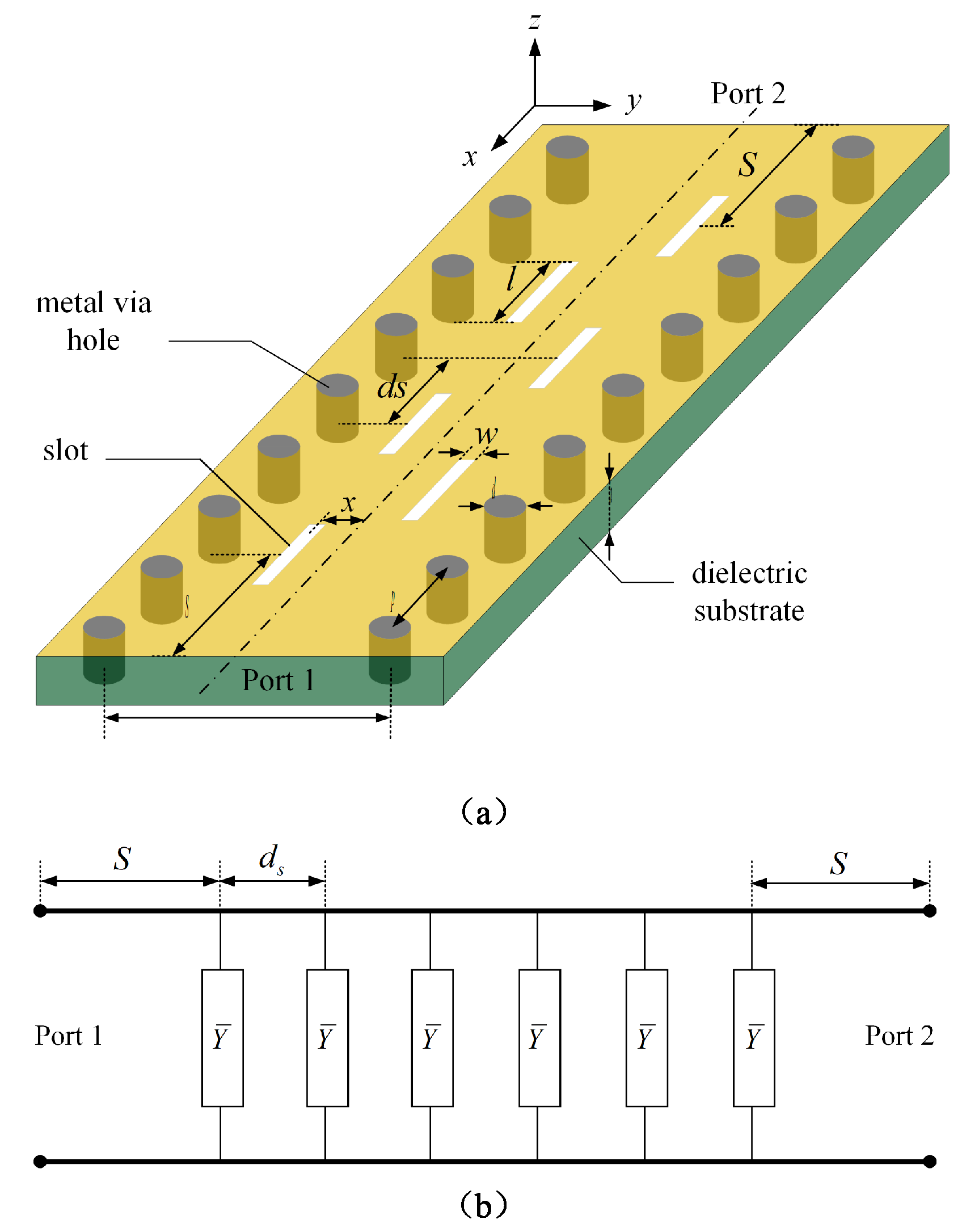
To calculate the equivalent admittance affected by the slot coupling in the linear array, an SIW analytical model with slots is considered. For example, Figure 1a shows the model with 6 slots. In this model, the spacing between slots is half of a waveguide wavelength . To maintain the phase consistency, slots are arranged alternately on either side of the center line with the slot offset x from the center line. The dielectric substrate material used is Rogers RO3003, which has a permittivity of 3 and a loss tangent of 0.0013 at 10 GHz. This material is sourced from Rogers Corporation in Rogers, Connecticut, USA. Depending on the engineering experience, the permittivity of Rogers RO3003 may vary slightly at 77 GHz. Therefore, the permittivity of the dielectric substrate used in simulation is adjusted to 3.07. At the operating frequency of 77 GHz, the parameters of the SIW are set as , , , and to satisfy the conditions of the single model transmission and lockage characteristics. The initial value of slots’ parameters are set as , , .

Figure 1.
(a) The equivalent admittance analytical model when . (b) The equivalent circuit of the model.
Figure 1b shows the equivalent circuit of the analytical model, and each slot is equivalent to a parallel normalized admittance . To obtain an expression of , the T transmission matrix is used. The T-matrix of the entire analysis system, the transmission line of length S and , and the normalized admittance are assumed to be , , , and , respectively. In a cascaded system, the T-matrix of the whole system can be viewed as the multiplicative form of the T-matrices of each part. The expression for each T-matrix is as follows:
In Equations (1) and (2), denotes the phase constant in model. In Equation (4), the matrix represents the Nth power of the matrix , and its expansion can be written as:
which can be improved by mathematical induction. The proof process is as follows:
When , the equation holds.
When ,
the equation holds.
Suppose that the equation holds when , :
When :
the equation holds. Thus, Equation (5) holds.
In Equation (4), the matrix can be calculated from the S-matrix , according to the relationship between the T-matrix and S-matrix:
Substituting Equations (5) and (9) into Equation (4):
According to , the equation of can be obtained as:
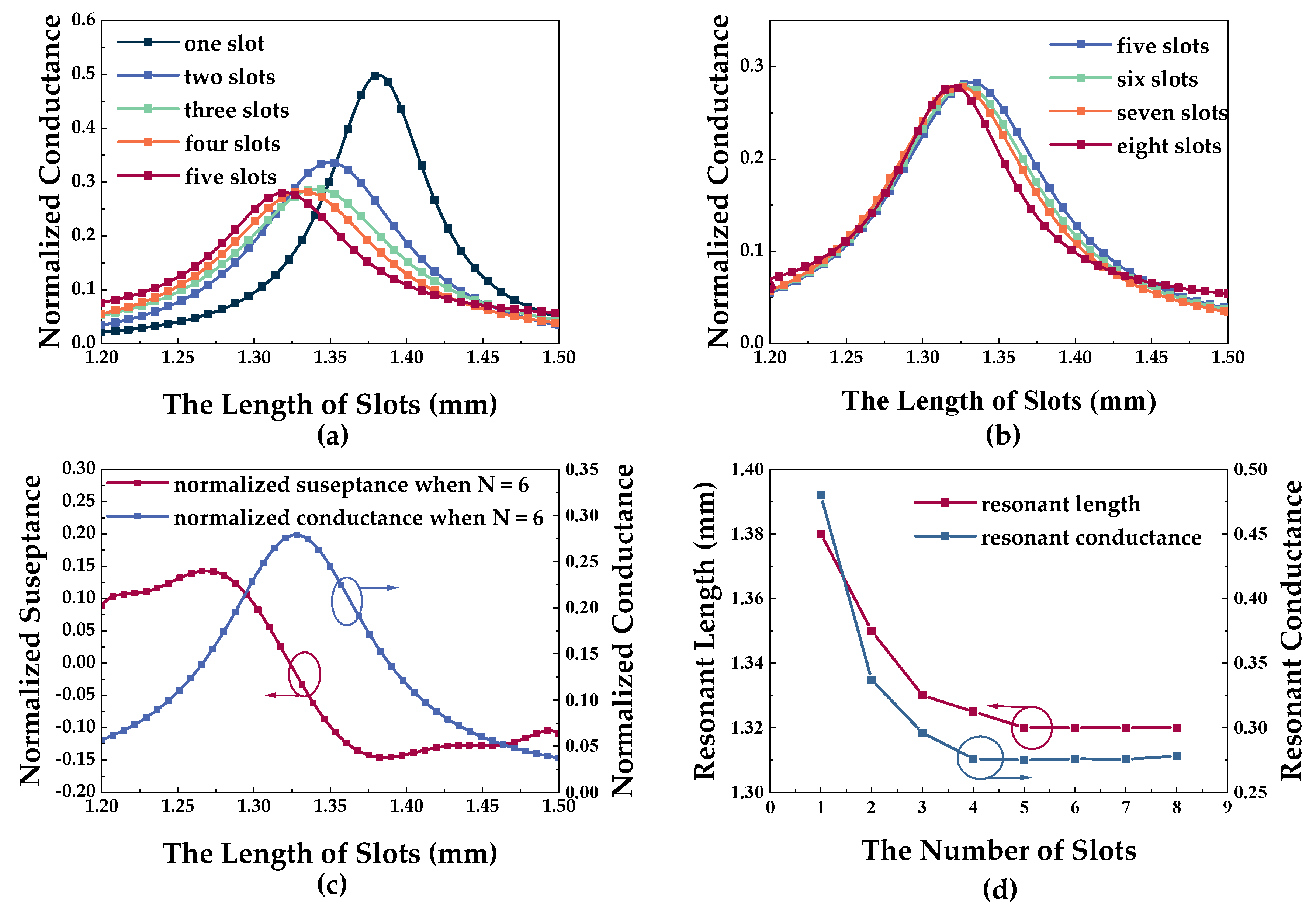
Using Equation (11), function curves of the normalized conductance and the normalized susceptance vary, with l being obtained while keeping x unchanged. For example, Figure 2 shows the measured data in different N when . Figure 2a,b show the function curves of vary with l when N varies from 1 to 5 and from 5 to 8, respectively. The resonant length makes reach its extreme points, and the resonant conductance of the slot can also be obtained. When the slot is in the resonant state, the susceptance is 0, and the radiation efficiency is the highest, as shown in Figure 2c. Figure 2d shows the curves of and as N changes. and keep decreasing with the increase in N, but when , the changes in and trend to stable. Furthermore, the results show that the impact of the slot coupling on the equivalent conductance increases with increasing N, while the resonant conductance and length decrease. When the number of slots reaches more than five, the coupling effect becomes negligible, indicating that the number of slots N, used in the analytical model, is at least five.
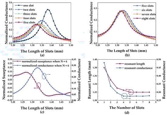
Figure 2.
Function curves at different N, with an offset of 0.2 mm. (a) Function curves of when N is from 1 to 5. (b) Function curves of when N is from 5 to 8. (c) Function curves of and l when N = 6. (d) Function curves of and vary with N.
By repeating the above process many times, the resonant conductance and resonant length under a different offset x can be obtained. Meanwhile, the fitting functions and can be constructed. The function describes the relationship between and x, and describes the relationship between and x. Figure 3a,b show the data curves of and calculated by different methods, respectively, which can be used in the low sidelobe SIW antenna design. The red curves are calculated by Equation (11) when and , respectively. The light green curves are calculated by the equation in [26] when N = 1 and . The red and light green curves show a high degree of agreement, which demonstrates the correctness of the method proposed in this work. In addition, the method in [26] is affected by the phase term associated with phase propagation constant and S, while the method proposed in this work is not affected by the phase term as shown in Equation (11). This is because the phase term is canceled out during the derivation due to the cascading nature of the T-matrix. The light blue curves are calculated by the method in [29] when N = 6 and q = 0.9905. In this method, q is a constant associated with the loss factor and length S. This method can calculate the conductance under the impact of the slot coupling but cannot obtain susceptance data. In contrast to the method in [29], the method proposed in this work not only can measure the conductance under the impact of the slot coupling but can also calculate the susceptance data. Moreover, this method is not affected by the constant q.
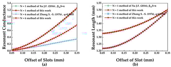
Figure 3.
Comparison of fitting functions with Refs. [37] (Xu J.F) and [40] (Zhong S. -S.). (a) The fitting function . (b) The fitting function .
In the design of low sidelobe waveguide slot antennas, Chebyshev or Taylor line source distributions are commonly utilized to ascertain the relative excitation distribution across individual slots. This facilitates the computation of the equivalent conductance for each slot. Subsequently, the fitting functions and that describe the relationship between resonant length, offset, and equivalent conductance are utilized effectively. They facilitate the determination of the length and offset of each slot. Consequently, the fitting functions depicted in Figure 3 assume a critical role in the forthcoming design endeavors.
2.2. The Antenna Design Process
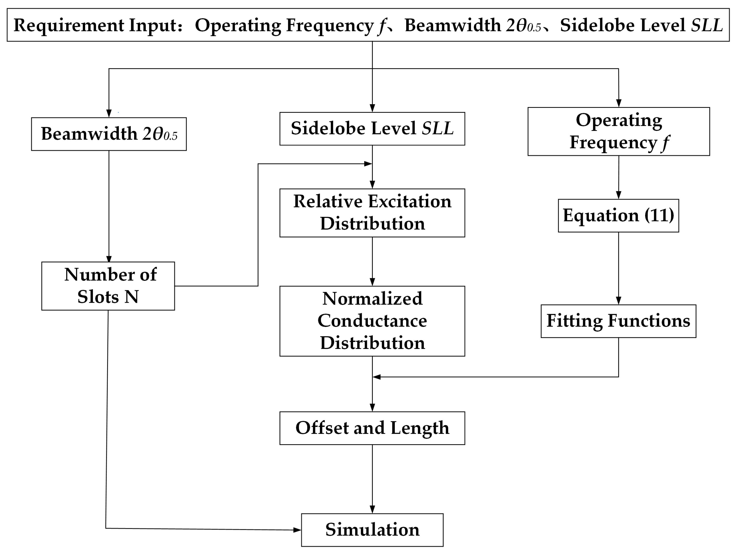
The design process of the low sidelobe SIW antenna can be summarized as follows:
- Give design requirements, including the operating frequency f, the beamwidth , and the sidelobe lever ;
- Calculate the number of slots N according to the beamwidth ;
- Establish the multislot simulated and analytical model and calculate the fitting functions and ;
- Calculate the normalized conductance of each slot using the Chebyshev or Taylor line source synthesis methods according to the sidelobe lever ;
- Calculate the offset and length of each slot according to normalized conductance and length fitting functions;
- Establish the antenna model, simulating model, and optimizing model.
The antenna design flow chart is shown in Figure 4.

Figure 4.
Antenna design flow chat.
3. Experiments and Results
3.1. Antenna Design and Simulation
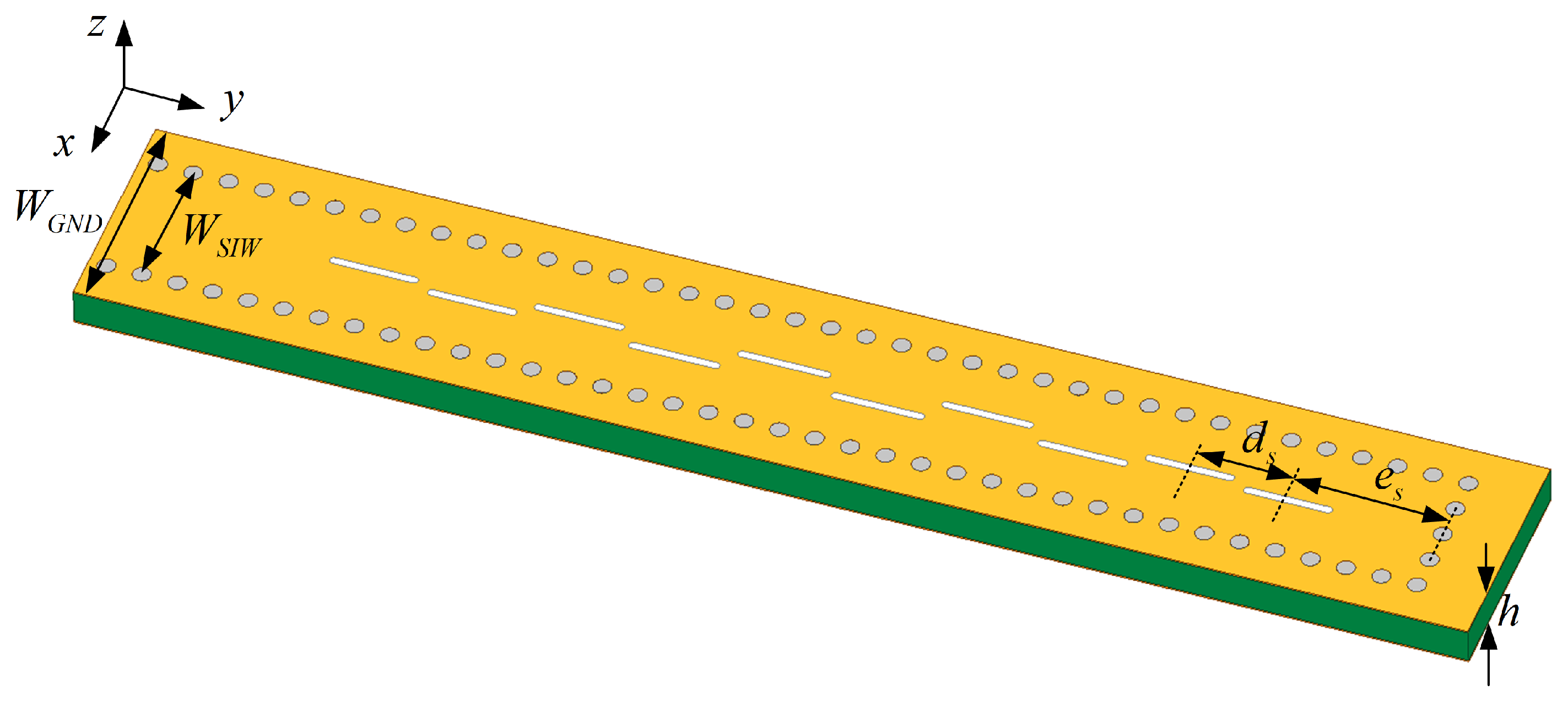
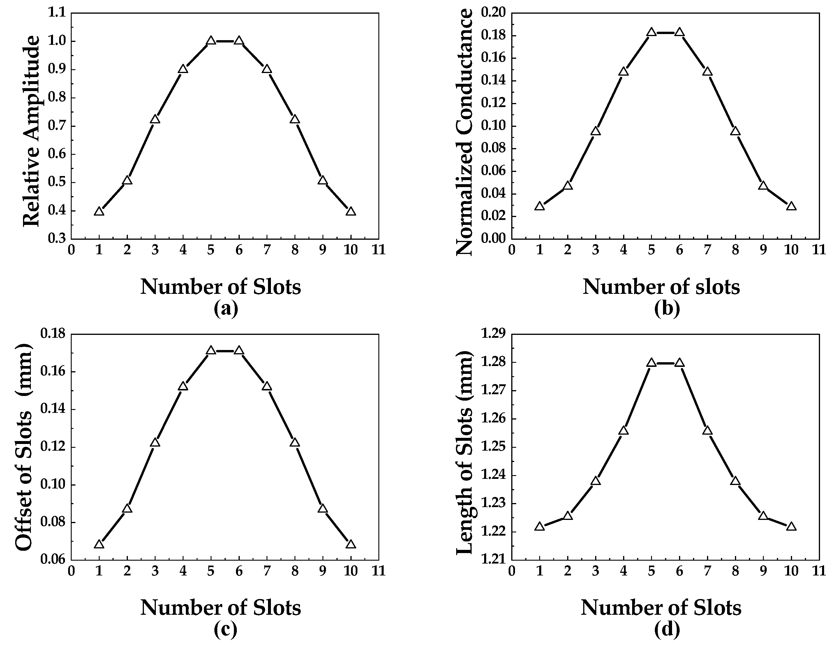
The requirements are set as: , , and . According to the beamwidth requirement, the number of slots N is 10, and the 10-element SIW longitudinal slot antenna model simulated in HFSS is shown in Figure 5. The parameters of SIW are the same as previously mentioned, and the width of the ground plane is . The dielectric substrate is Rogers RO3003 with a thickness of 0.508 mm. The slots are numbered 1 to 10 from left to right. To satisfy the standing wave transmission condition, the distance from the tenth slot to the short-circuit is . The spacing between slots is to maintain phase consistency and the width of each slot is 0.11 mm. To meet the requirement of and prevent current mutations at both ends, 10-element Chebyshev weighting is used, and Figure 6a shows the relative amplitude of each slot. For the longitudinal slot antennas, each slot can be equivalent to the parallel conductance in the transmission line. Assuming the normalized conductance of the ith slot is , can be expressed as:
where K is a constant, and is the relative amplitude of the ith slot. To achieve great impedance matching, the input normalized conductance should be 1:

Figure 5.
The SIW longitudinal slot antenna diagram.

Figure 6.
(a) Relative current excitation distribution of slots. (b) Normalized conductance distribution of slots. (c) Offset of slots. (d) Length of slots.
Through calculation, the normalized conductance value distribution of slots is shown in Figure 6b. Furthermore, according to the fitting functions and when N = 6 shown in Figure 3, the offset and length of each slot can be obtained. Eventually, the offset and length of each slot are shown in Figure 6c and d, respectively. Moreover, the concrete parameters of slots are shown in Table 1.

Table 1.
The length and offset of each slot.
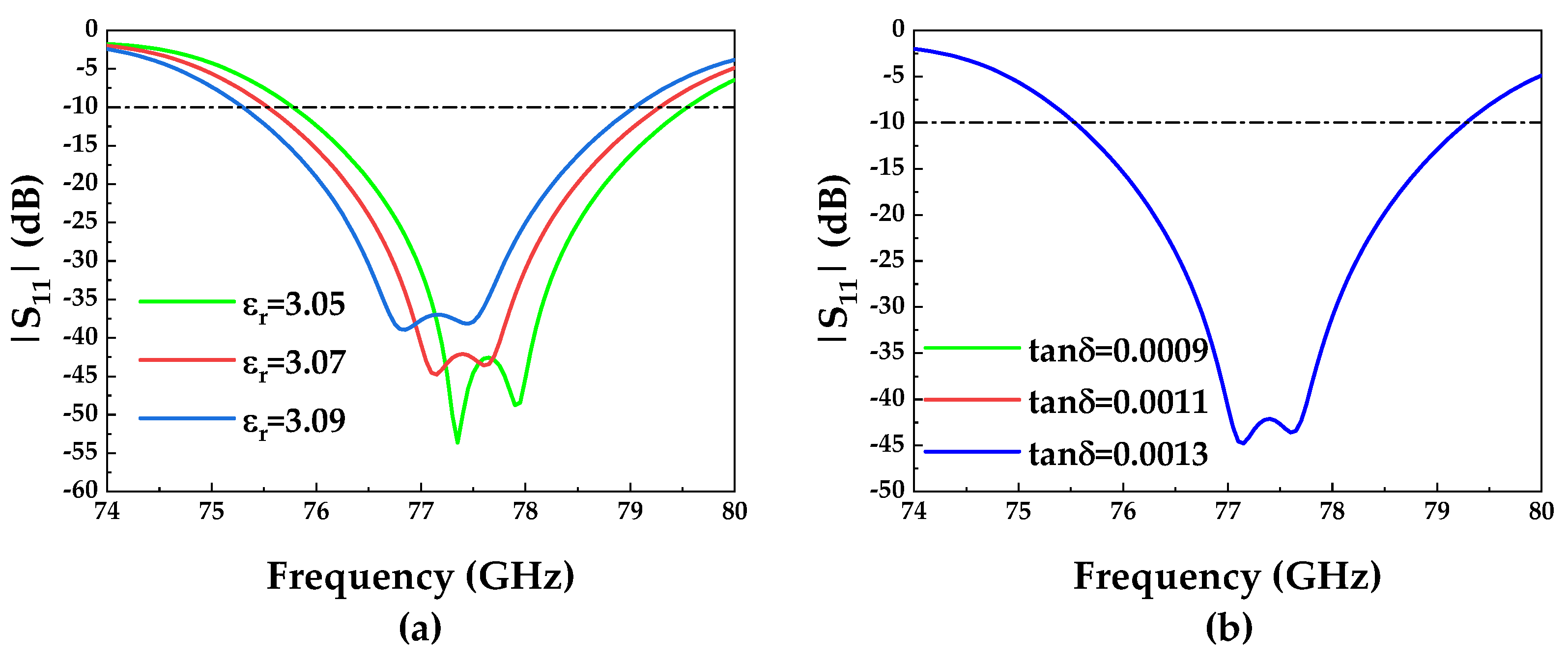
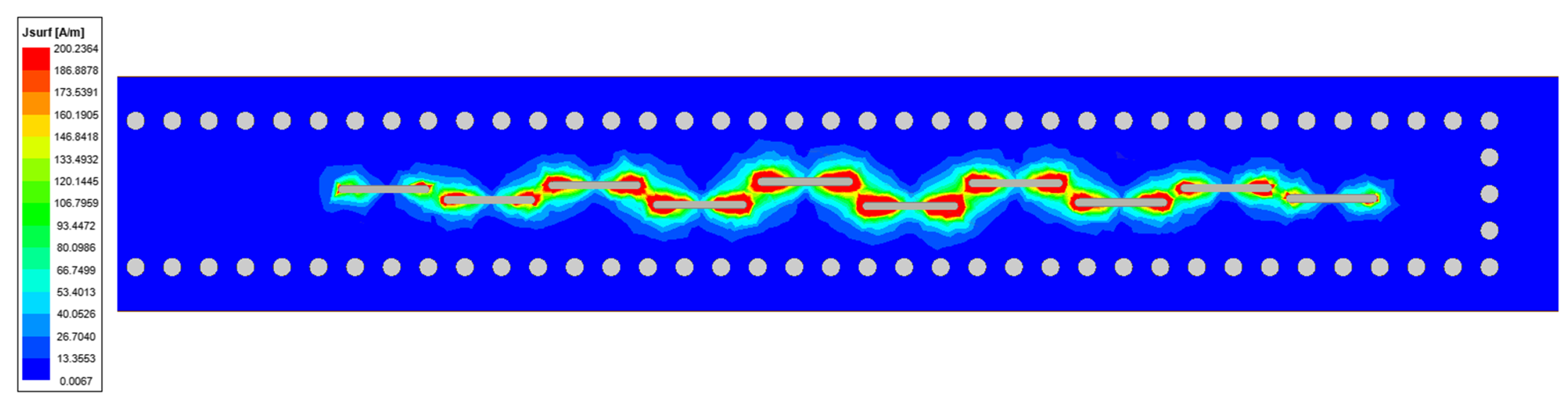
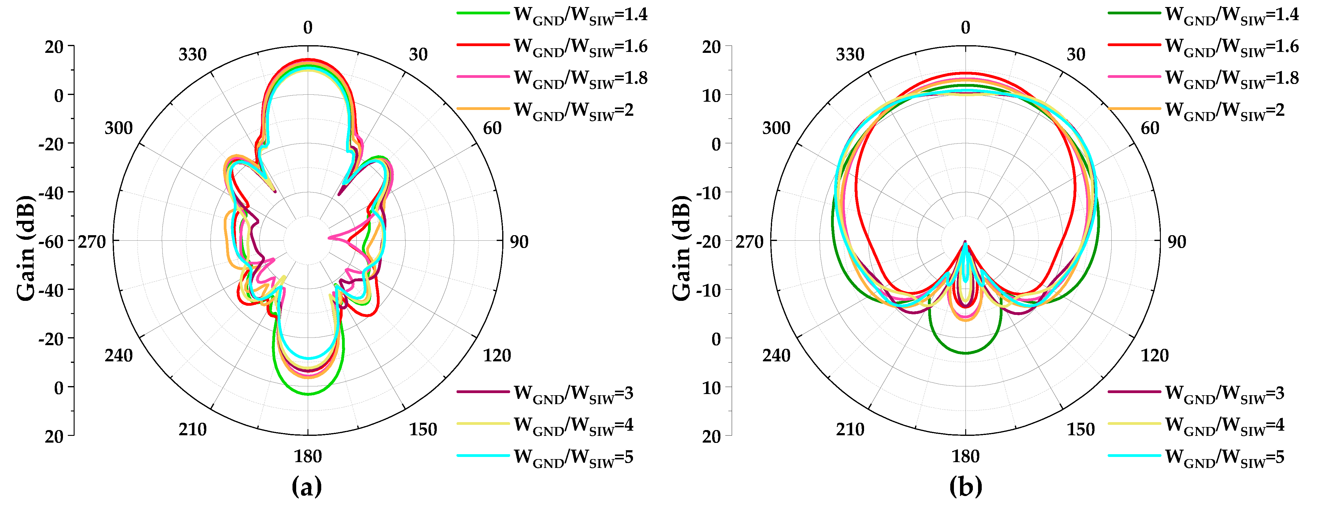
The simulation results are shown in Figure 7 and Figure 8. Figure 7 shows for the low sidelobe antenna. The proposed design achieves excellent impedance matching at 77 GHz, exhibiting a frequency impedance bandwidth of 4.8%. Figure 7a indicates that changes in the permittivity affect the operating frequency of the antenna. Furthermore, Figure 7b shows that the tuning performance is not influenced by variations in the dielectric loss tangent. Figure 8 illustrates the normalized radiation patterns in both the H-plane and E-plane at 77 GHz. Based on the simulation results, the antenna achieves a gain of 13.2 dBi. The beamwidth is measured at 64° in the E-plane and 17° in the H-plane. Additionally, the antenna exhibits an SLL of −29 dB in the H-plane. Both the beamwidth and SLL meet the specified requirements. Furthermore, Figure 9 presents the surface current distribution at 77 GHz highlighting noticeable amplitudes in slot regions. It is noteworthy that an alteration in the the ground plane width induces variations in the radiation patterns, as depicted in Figure 10 showcasing these variations through the width ratio. According to the simulation results, the alteration has a large impact on the gain, and there is a suitable ratio to maximize it. The H-plane pattern is found to be less affected by the ratio change, as depicted in Figure 10a. However, the E-plane pattern exhibits a significant sensitivity to the ratio change, as illustrated in Figure 10b. Particularly for extremely large ratios, there is a notable reduction in gain and substantial widening of the beamwidth in the E-plane. Moreover, the E-plane beam fluctuates in the direction of the primary radiation. The primary factor contributing to this phenomenon is the transverse motion of the surface current. As the width of the ground plane increases, the current path also increases and the superposition of current phases significantly influences the radiation intensity in the E-plane. Moreover, the variation in the S-parameter affected by the width variation is shown in Figure 11. The impedance matching remains excellent despite the variation width.
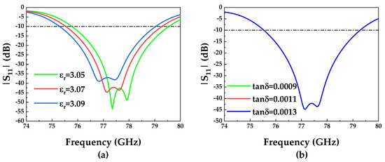
Figure 7.
Simulated against frequency (a) with different permittivity ; (b) with different loss tangent tan.
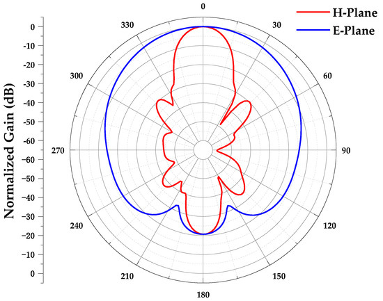
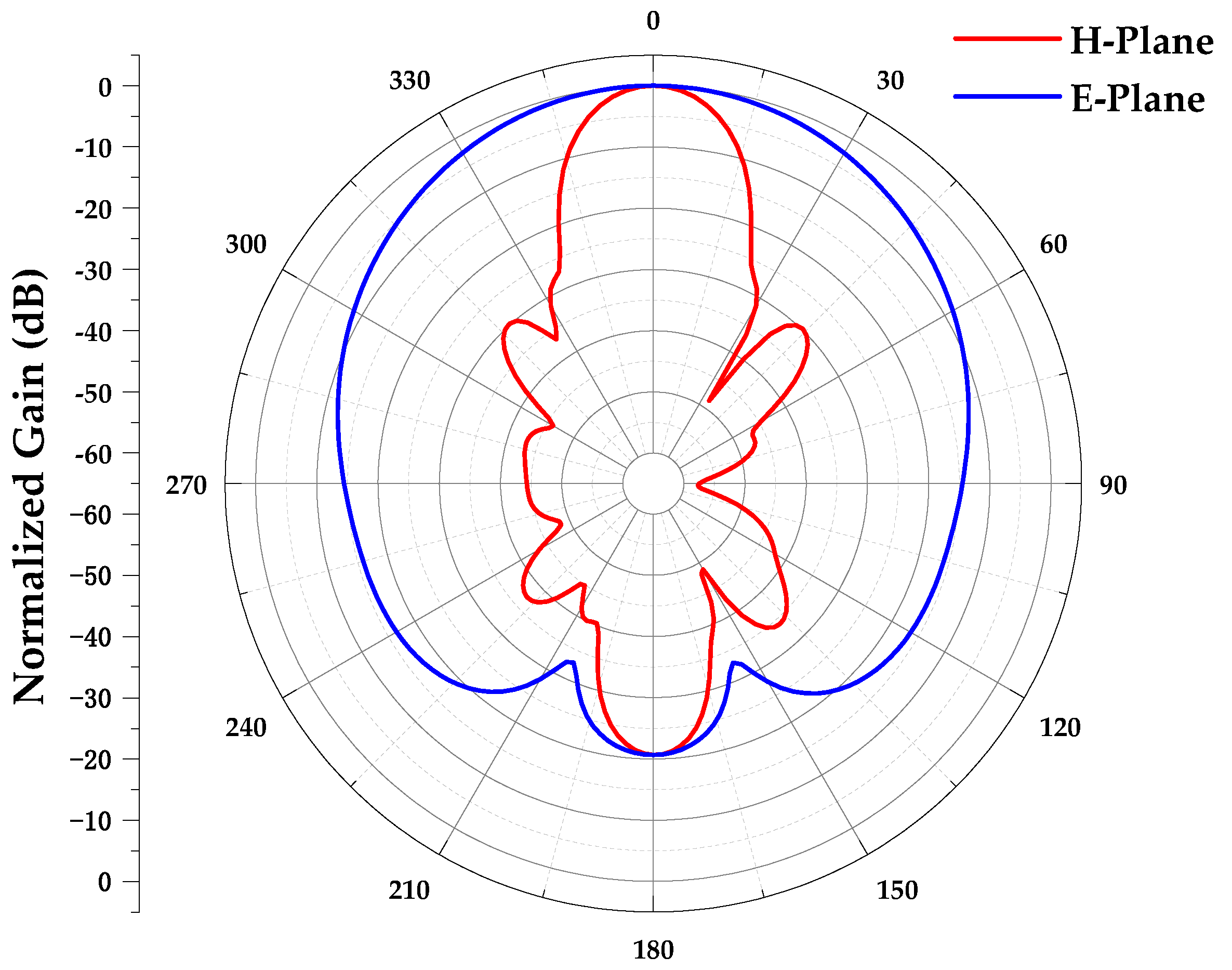
Figure 8.
Normalized radiation patterns at 77 GHz.
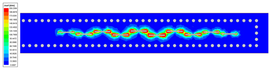
Figure 9.
The surface current distribution at 77 GHz.
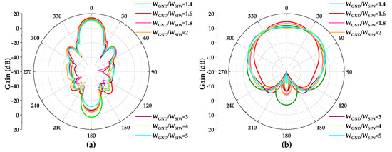
Figure 10.
The radiation patterns vary with at 77 GHz. (a) H-plane. (b) E-plane.
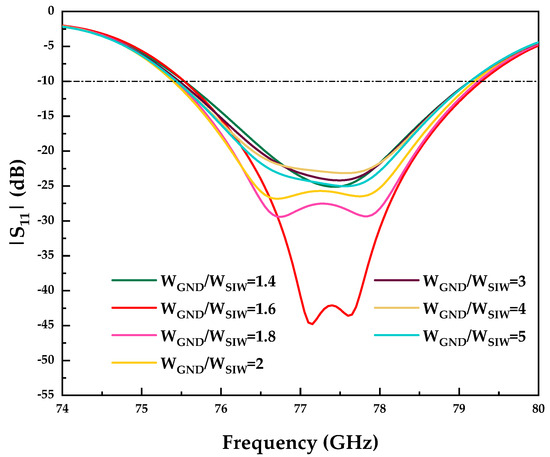
Figure 11.
The simulated vary with .
3.2. The Design of the Transition from RWG to SIW
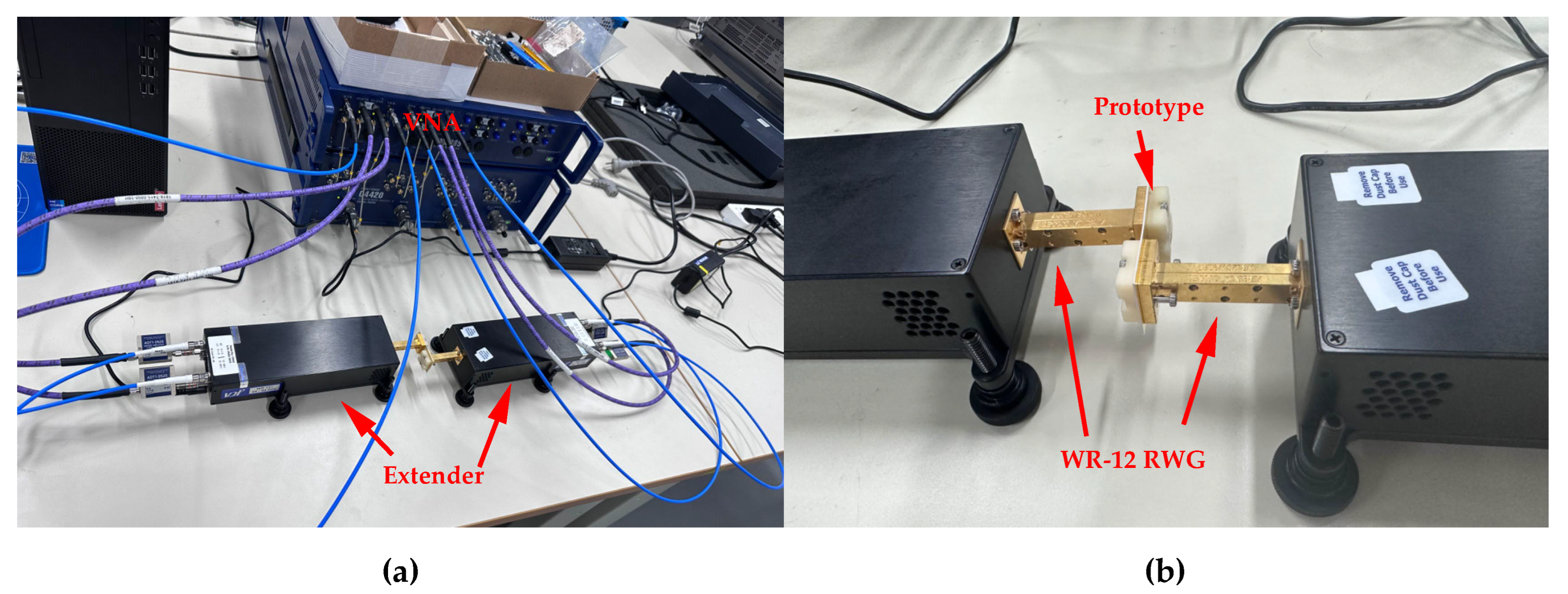
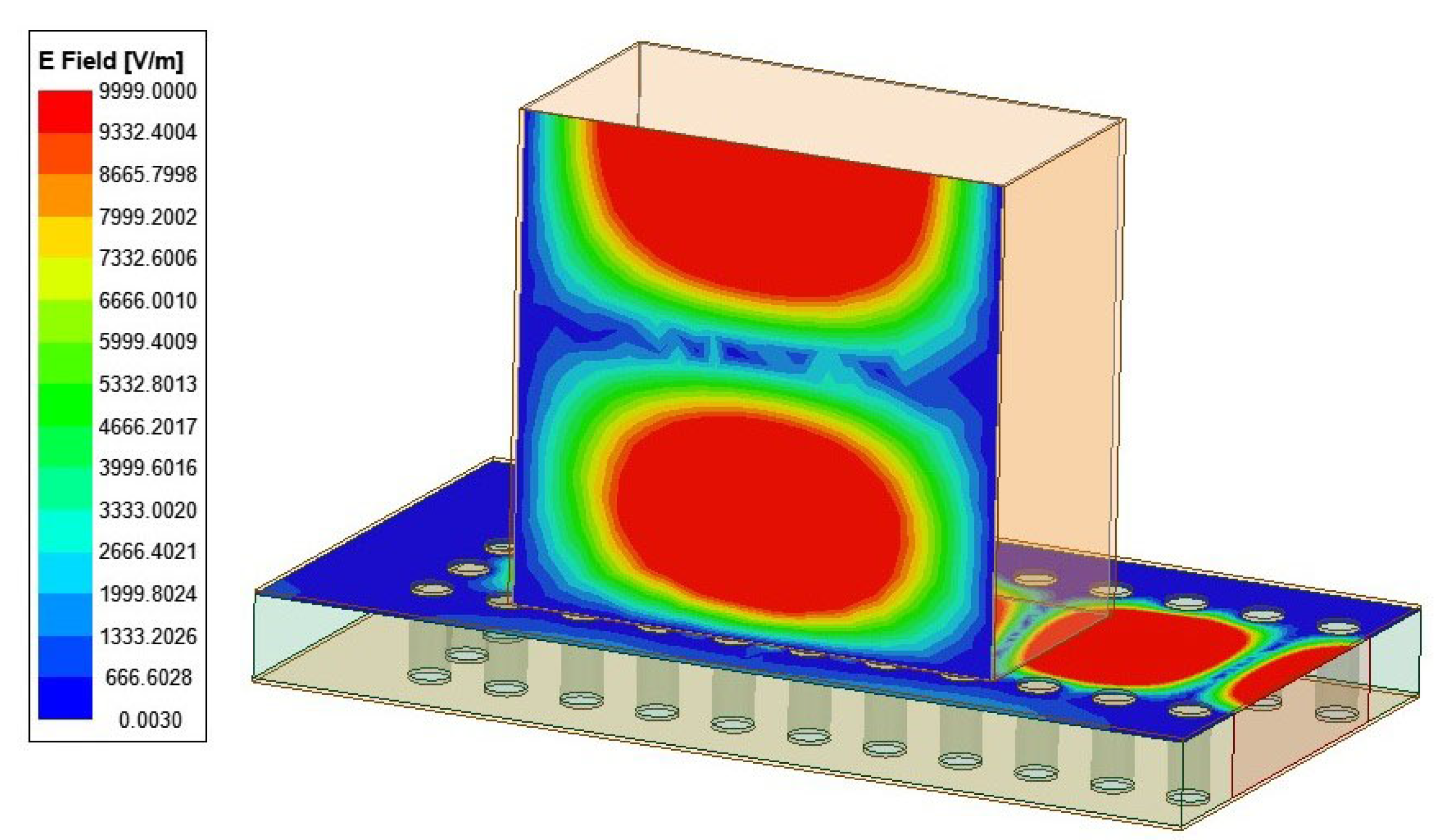
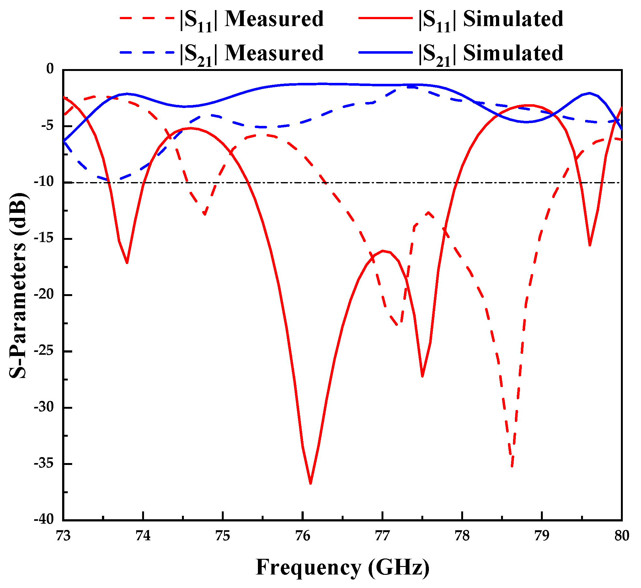
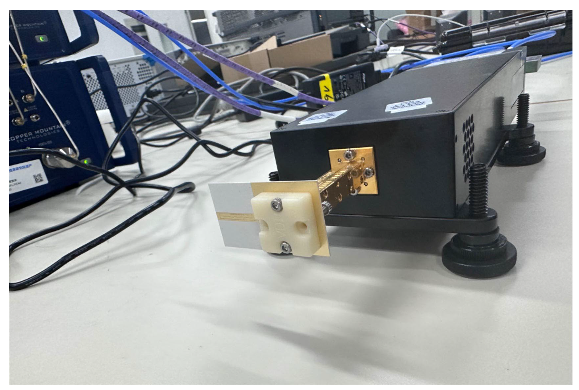
To measure the antenna at millimeter-wave frequencies, a transition from RWG to SIW is designed. Using fitting functions of one signal slot proposed in Section 2, a coupling slot structure transition can be designed easily. By setting the equivalent normalized conductance of the coupling slot as 1, the length and offset of the slot can be obtained by using Figure 3. The simulation model and parameters of the transition are presented in Figure 12a. The length, offset, and width of the coupling slot are 1.5 mm, 0.3 mm, and 0.11 mm, respectively, and the distance between the coupling slot and short-circuit is . In Figure 12b, the transition is connected with a standard WR-12 waveguide. A vector network analyzer (VNA) and extenders are used to measure the S-parameters as shown in Figure 13. The simulation result of the electrical field transmission is illustrated in Figure 14, and it can realize the transformation from the vertical mode of the RGW to the transverse model of the SIW. The simulated S-parameters for the simulation model are illustrated in Figure 15. The transition has a great impedance matching at 77 GHz with a 4.1% frequency impedance bandwidth, and the insert losses in the bandwidth are less than 1 dB. To measure the transition, a prototype is manufactured as shown in Figure 12c,d. The simulation and measurement results of the prototype are shown in Figure 16. According to the results, the measurement results of are coincident with the simulation results, but the operating frequency of the measurement results move slightly toward the higher frequency. The main reasons are as follows:
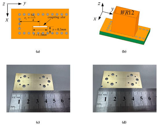
Figure 12.
(a) The structure of the transition. (b) The transition with standard WR-12. (c) The top view of the prototype. (d) The bottom view of the prototype.

Figure 13.
Photograph of the measurement. (a) Vector network analyzer (VNA) and extender. (b) The prototype connected with WR-12 standard rectangular waveguide (RWG).
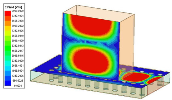
Figure 14.
The electric field mode transition.
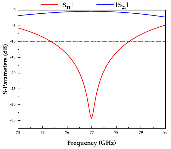
Figure 15.
The simulation results of the simulation model in Figure 12b.

Figure 16.
The simulation and measurement results of the prototype in Figure 12c,d.
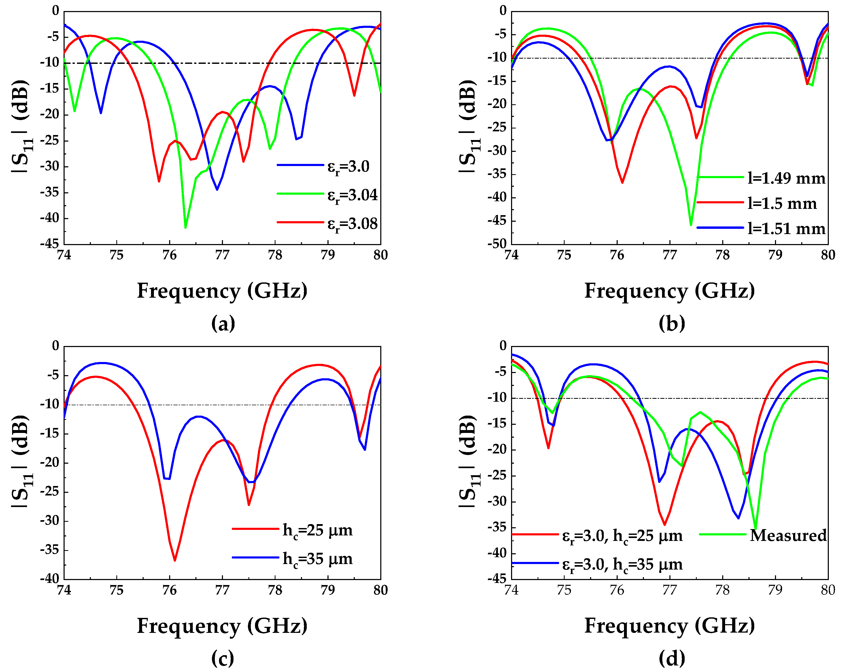
- The variation in the permittivity results in a shift in the operating frequency. The dielectric substrate employed in this work is Rogers RO3003, which exhibits a permittivity of 3.0 at 10 GHz. Drawing on engineering experience, the permittivity of this material fluctuates within a range of 3.0 to 3.12 at 77 GHz. In simulations, the permittivity is set as 3.07 in this work. Figure 17a illustrates the impact of permittivity variation on . The simulation results indicate a decrease in operating frequency as the permittivity increases. Therefore, the actual measured permittivity values should be less than the simulated permittivity values, which leads to a shift in measured operating frequency.
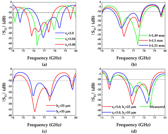 Figure 17. Error simulation analysis. (a) varies with permittivity . (b) varies with the length of slot l. (c) varies with the thickness of copper layer . (d) Simulated and measured .
 - Manufacturing errors have a certain impact on impedance matching. Figure 17b illustrates the impact of the length l variation of slots on . While this variation influences the impedance matching, it does not affect the operating frequency.
- The variation in the copper layer thickness influences the performance. The metallization via holes results in an approximate 10 m increase in the thickness of the copper layer. Figure 17c shows the impact of this variation on , leading to a slight shift in the operating frequency.
In summary, the variation in permittivity is the primary reason for the shift in the operating frequency. Figure 17d presents a comparison between the simulation and measurement results when the simulated permittivity is 3.0, showing a great agreement.
3.3. Simulation and Measurement Results
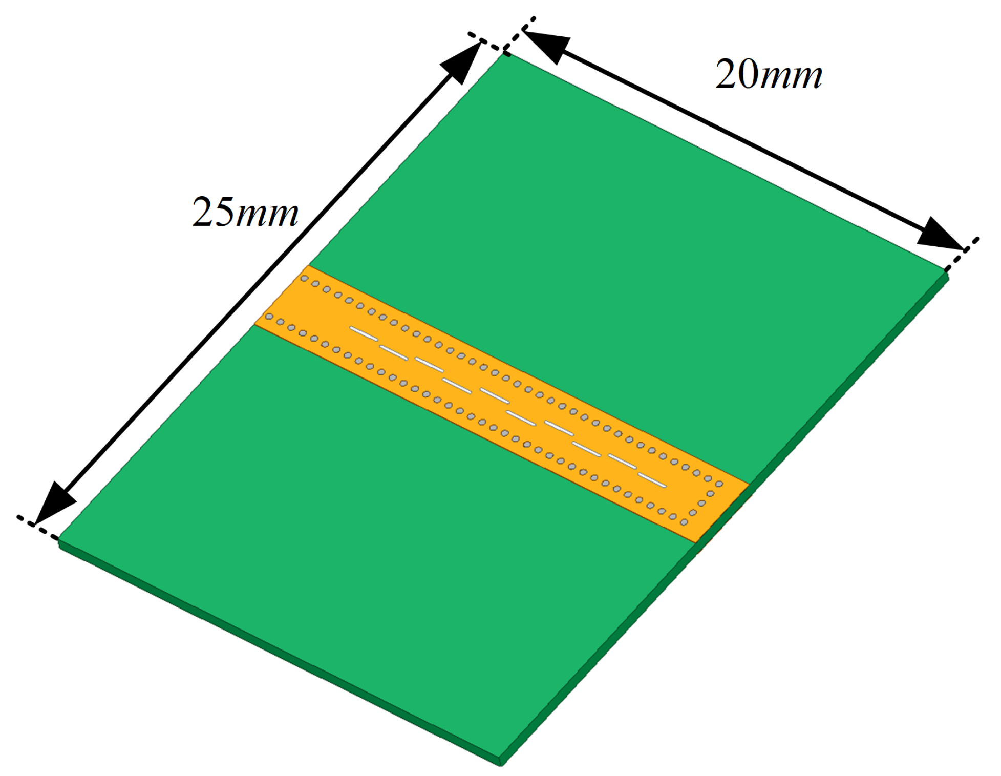
According to Figure 11, a suitable width ratio should be chosen to maximize the antenna gain. In addition, the width of the dielectric substrate is expanded to 25 mm to replicate the influence of the millimeter-wave radar printed circuit board (PCB) on the antenna, as shown in Figure 18. The antenna simulation model connected with transition is shown in Figure 19a,b. Figure 19a shows the top view of the antenna with radiating slots, and Figure 19b shows the bottom view of the antenna with a coupling slot as the transition from a standard RWG to SIW. Furthermore, to measure the actual performance of the antenna, a prototype is manufactured using the PCB process. Figure 20a,b show the top view and bottom view of the prototype, respectively.
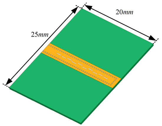
Figure 18.
The antenna simulation model without transition.
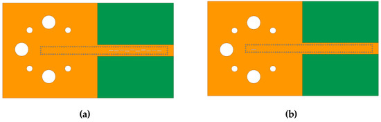
Figure 19.
The antenna simulation model with transition. (a) Top view. (b) Bottom view.
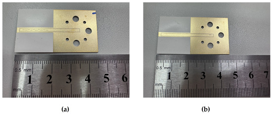
Figure 20.
Photograph of the prototype. (a) Top view. (b) Bottom view.
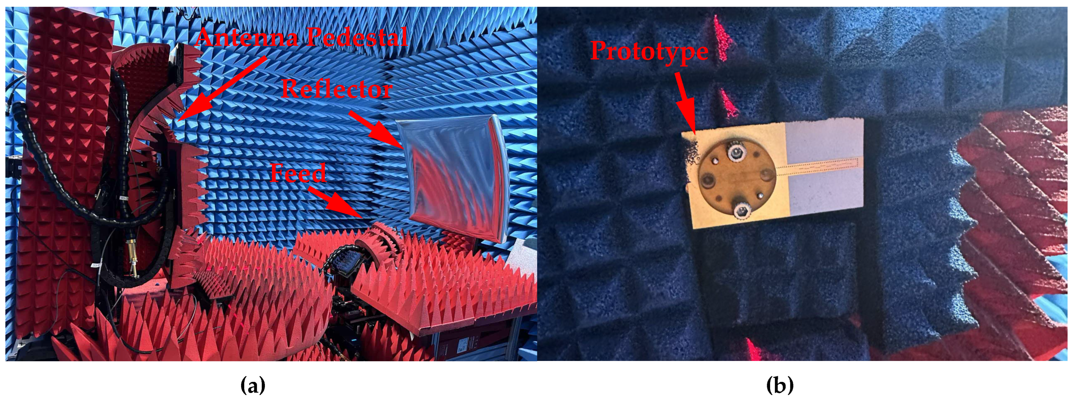
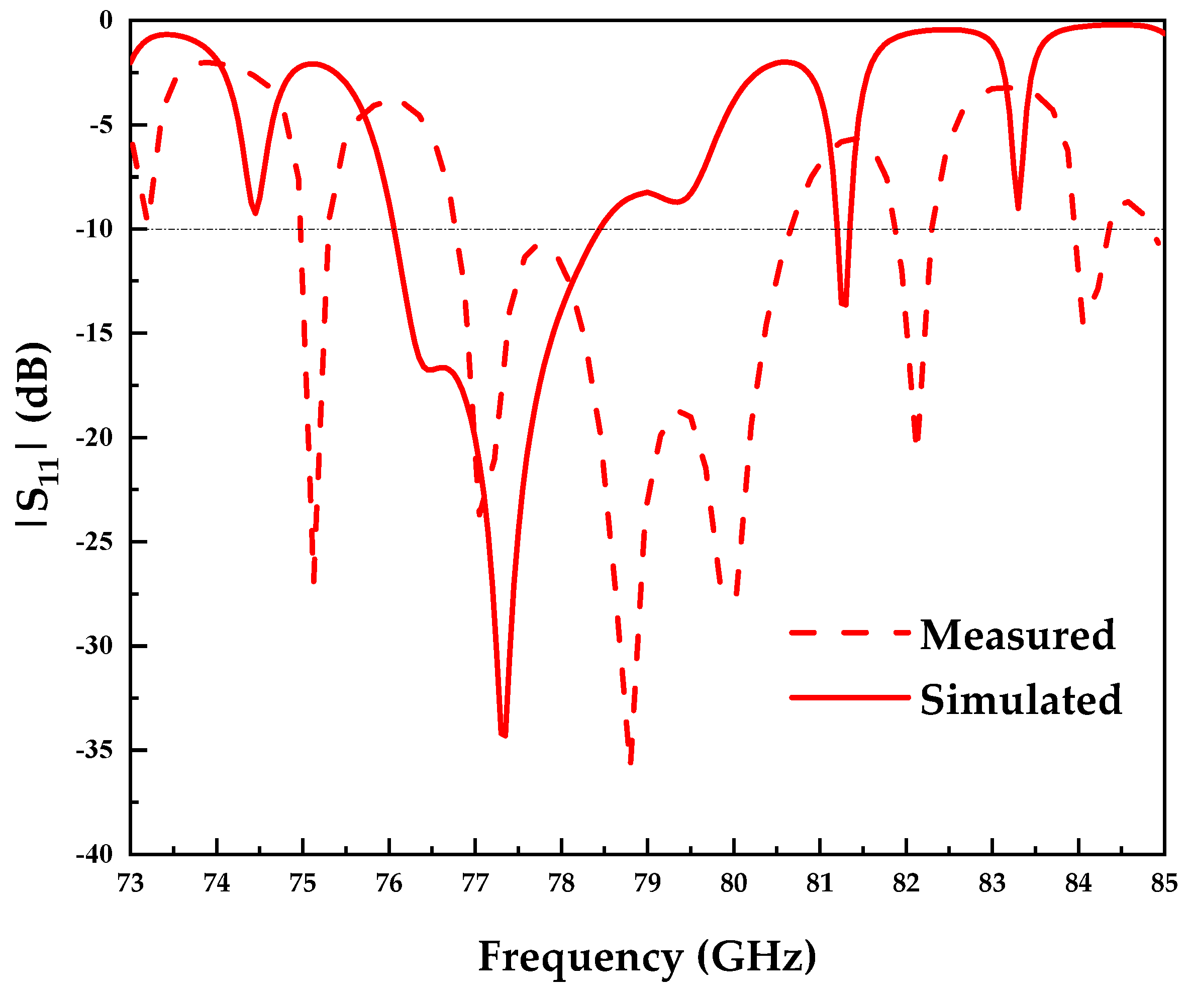
The same vector network analyzer (VNA) and extender with a WR-12 waveguide are used to measure the prototypes (as shown in Figure 21). And to measure the gain and radiating patterns of the antenna, a compact antenna test range (CATR) is used (as shown in Figure 22). The simulated and measured are shown in Figure 23. According to these results, the measured are coincident with the simulated results, but the resonant frequency of the measured results moves slightly toward the higher frequency. The specific reasons have been mentioned above. The simulated relative impedance bandwidth is 2.5%, and the measured relative impedance bandwidth is 5%.
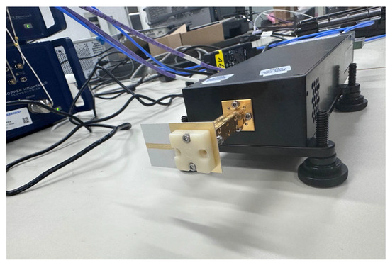
Figure 21.
The measurement for S-parameters.

Figure 22.
The measurement for radiating pattern. (a) The compact antenna test range (CATR). (b) The measured prototype.
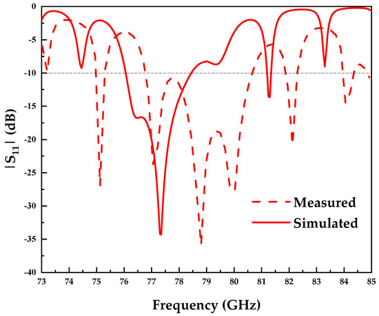
Figure 23.
The simulated and measured .
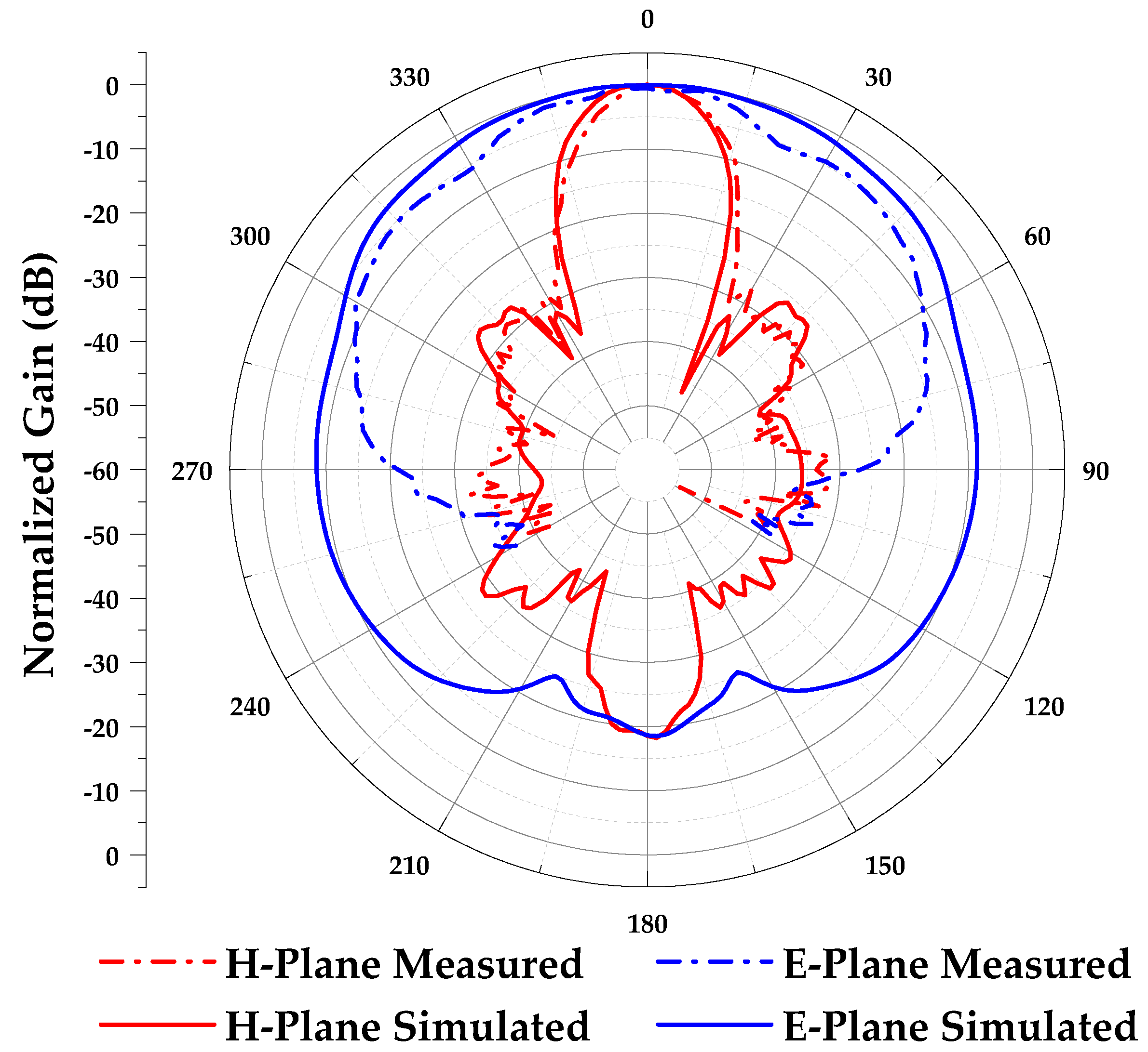
The simulated and measured radiating patterns are shown in Figure 24. The simulated gain is 12.5 dBi, and the simulated gain is reduced by 2 dBi compared to the simulated results in Section 3.2. The main reasons are the widening of the dielectric substrate width and the insertion losses of the transition. The measured gain is 10.2 dBi, and the insertion loss of the measurement equipment link results in the decrease in the measured gain. In H-plane, both the simulated and measured beamwidths are 17°, and both the simulated and measured SLLs are less than −28 dB. The accuracy of the conductance calculation is evidenced by the low sidelobe level.
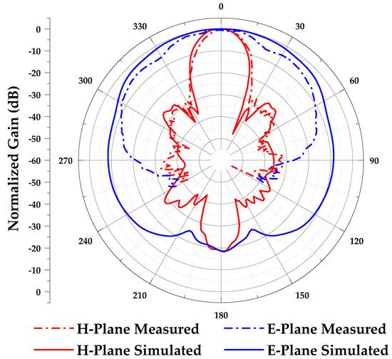
Figure 24.
The simulated and measured normalized radiating patterns at 77 GHz.
In the E-plane, there are quite a few differences between the simulated and measured normalized radiating patterns at a large angle, and the primary reason is attributed to the electromagnetic wave obstruction by the absorbing materials. As shown in Figure 22, the antenna pedestal and the antenna were surrounded by numerous absorbing materials. These materials were used to prevent reflections from the metal of the antenna pedestal from affecting the measurement results. Therefore, when the antenna and pedestal rotated to a large degree, the absorbing materials absorbed and blocked a portion of the electromagnetic wave, leading to a reduction in the power of the electromagnetic wave received by the antenna. This phenomenon explains why the measured gain began to decrease when the rotation angle exceeded 60 degrees, particularly in the E-plane. Moreover, when the rotation angle surpassed 120 degrees, the electromagnetic waves were almost entirely occluded by the absorbing materials.
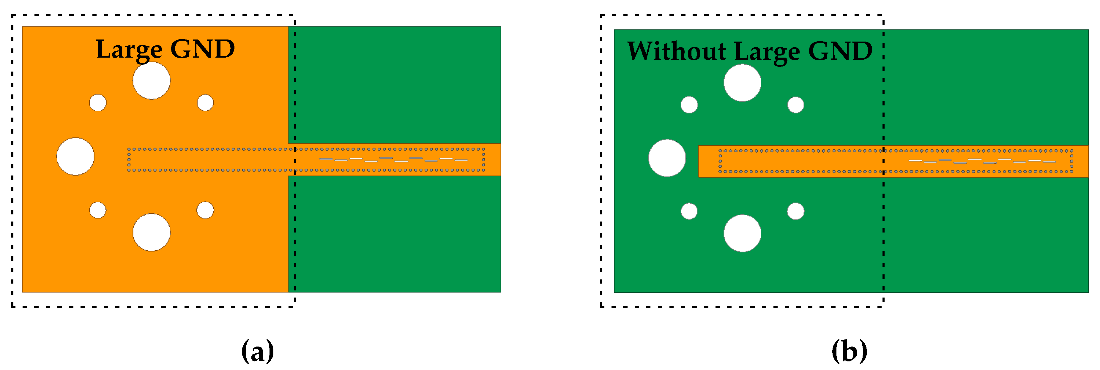
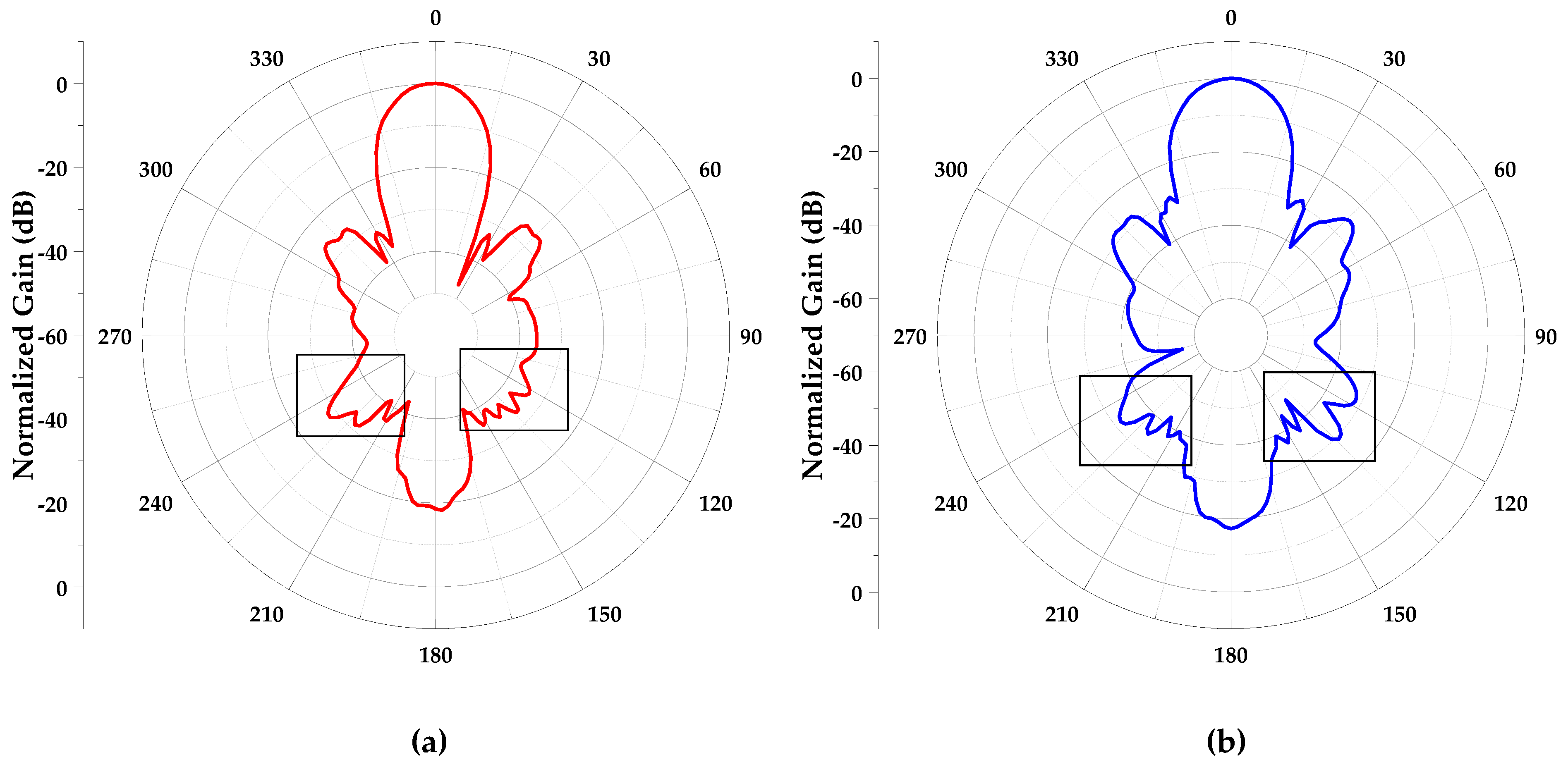
As depicted in Figure 24, there is a slight asymmetry in the H-plane radiation pattern, notably within the ranges of 210 to 240 degrees and 120 to 150 degrees. Within these intervals, a discernible difference in gain is evident. This phenomenon is predominantly influenced by the presence of the larger GND in the antenna model. To corroborate this observation, a simulation model without a large GND was executed. Figure 25 demonstrates the two simulation models, with and without the large GND. Figure 26a,b show the simulation results of antenna models with GND and without GND, respectively. Based on the comparative results (areas circled by squares), the asymmetry in the radiation pattern was mitigated upon the removal of the ground plane (GND).

Figure 25.
Simulation models. (a) With a large GND. (b) Without a large GND.
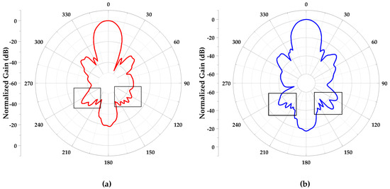
Figure 26.
Simulated normalized radiating patterns in H-plane. (a) With a large GND. (b) Without a large GND.
The comparison of the results with related references is shown in Table 2, underscoring the superiority of the methodology introduced in this paper. According to the table, the antenna designed in this paper, compared with those in other references with the same number of elements, exhibits higher gain and lower sidelobe levels. This underscores the superiority of the method proposed in this study.
Table 2.
The comparison with related references.
4. Discussion
In millimeter-wave radar systems, antenna performance critically sets the upper limit for the overall system capabilities. Microstrip antennas commonly employed in these systems confront substantial challenges, including high loss and severe surface wave effects. Conversely, substrate-integrated waveguide (SIW) longitudinal slot antennas offer significant advantages, such as low loss and high power capacity. In addition, these antennas are also immune to the effects of surface waves. Therefore, SIW longitudinal slot antennas hold tremendous potential in millimeter-wave radar systems.
This study focuses on SIW longitudinal slot antennas suitable for millimeter-wave radar applications. A novel design method is proposed to reduce the sidelobe levels of SIW longitudinal slot antennas. This method addresses the issue of slot equivalent conductivity being affected by slot coupling. At its core, it introduces a new equation for calculating conductivity under coupling effects. Based on this equation, fitting functions for conductivity and resonant length variation with offset are calculated. Using these functions, a low sidelobe SIW antenna with ten elements and a waveguide-to-SIW transition structure is designed. The antenna demonstrates an exceptionally low sidelobe level of −28 dB and a gain of 13.2 dBi. Compared to antennas of similar size, it shows higher gain and lower sidelobe levels. This indicates that the design method proposed in this paper effectively reduces the residual inductance of the resonant slot, leading to higher operational efficiency and gain in the antenna. Both simulation and experimental results suggest that the antenna designed in this study is highly suitable for millimeter-wave radar applications.
However, despite achieving an exceptionally low sidelobe level, the antenna has a relatively small front-to-back ratio. This is primarily due to the diffraction of lateral currents leaking from the slots at the edges of the antenna. The currents diffracted to the back of the antenna combine, resulting in a significant back lobe. This larger back lobe caused by current diffraction is an inherent issue due to the waveguide antenna structure. Although experiments have shown that this phenomenon is significantly improved in MIMO array applications of millimeter-wave radars, how to effectively reduce the back lobe of SIW antennas remains a pertinent issue for future research.
5. Conclusions
This study introduces a novel strategy for designing low sidelobe SIW longitudinal slot antennas. The approach centers on deriving fitting functions for resonant conductance and resonant length, considering the impact of slot coupling. Leveraging these functions, a design encompassing an RWG to SIW transition and a low sidelobe SIW antenna is developed. The outcomes show that the design approach meets the −25 dB SLL target, with empirical measurements indicating SLL values lower than −28 dB. Both simulation and real-world test results affirm the method’s precision and superiority. Despite its success in achieving low sidelobes, the antenna exhibits a small front-to-back ratio. Addressing the challenge of reducing the prominent back lobe presents a valuable direction for future research.
Author Contributions
Conceptualization, S.W. and B.Z.; methodology, S.W. and B.Z.; software, S.W. and B.Z.; validation, S.W. and B.Z.; formal analysis, S.W., B.Z. and G.F.; investigation, B.Z. and G.F.; resources, B.Z. and G.F.; data curation, B.Z. and G.F.; writing—original draft preparation, S.W.; writing—review and editing, B.Z.; visualization, S.W.; supervision, G.F.; project administration, B.Z. and G.F.; funding acquisition, B.Z. and G.F. All authors have read and agreed to the published version of the manuscript.
Funding
This research was funded by the National Natural Science Foundation of China, grant number 61988102, by the Key Research and Development Program of Guangdong Province, grant number 2019B090917007, and by the Science and Technology Planning Project of Guangdong Province, grant number 2019B090909011.
Data Availability Statement
The data presented in this study are available on request from the corresponding author. The data are not publicly available due to privacy.
Acknowledgments
The authors sincerely thank the editors and reviewers for their efforts in the publication of this paper.
Conflicts of Interest
The authors declare no conflicts of interest.
References
- Hirokawa, J.; Ando, M. Single-layer feed waveguide consisting of posts for plane TEM wave excitation in parallel plates. IEEE Trans. Antennas Propag. 1998, 46, 625–630. [Google Scholar] [CrossRef]
- Hiroshi, U.; Takenoshita, T.; Fujii, M. Development of a laminated waveguide. IEEE Trans. Microw. Theory Tech. 1998, 12, 2438–2443. [Google Scholar]
- Deslandes, D.; Wu, K. Integrated Microstrip, and Rectangular Waveguide in Planar Firm. IEEE Microw. Guid. Wave Lett. 2001, 11, 68–70. [Google Scholar] [CrossRef]
- Xu, F.; Wu, K. Guided-wave and leakage characteristics of substrate integrated waveguide. IEEE Trans. Microw. Theory Tech. 2005, 53, 66–73. [Google Scholar]
- Li, L.; Zhang, C.; Qiao, X.; Shao, Y. A Broadband SIW-Fed Rhombic Loop Antenna with Endfire Radiation for Millimeter-Wave Applications. IEEE Antennas Wirel. Propag. Lett. 2022, 21, 1293–1297. [Google Scholar] [CrossRef]
- Chen, Y.; Zhang, L.; He, Y.; Mao, C.; Wong, S.; Li, W.; Chu, P.; Gao, S. Broadband High-Gain SIW Horn Antenna Loaded with Tapered Multistrip Transition and Dielectric Slab for mm-Wave Application. IEEE Antennas Wirel. Propag. Lett. 2022, 70, 5947–5952. [Google Scholar] [CrossRef]
- Alistarh, C.; Anitori, L.; van Rossum, W.L.; Podilchak, S.K.; Thompson, J.; Sellathurai, M. Compressed Sensing for MIMO Radar using SIW Antennas for High Resolution Detection. In Proceedings of the 2021 18th European Radar Conference (EuRAD), London, UK, 5–7 April 2022; pp. 485–488. [Google Scholar]
- Gao, D.; Li, S.; Chen, A.Y.-K.; Wu, C.-T.M. A W-band Self-Injection-Locked Vital Sign Radar Sensor with On-Chip SIW Monopole Antenna in 0.1-µm GaAs pHEMT. In Proceedings of the 2023 IEEE/MTT-S International Microwave Symposium, San Diego, CA, USA, 11–16 June 2023; pp. 871–874. [Google Scholar]
- Yamamoto, S.I.; Hikono, N.; Hirokawa, J.; Ando, M. A 120-degree beamwidth post-wall waveguide slot array with a three-way power divider on a single-layer dielectric substrate. In Proceedings of the IEEE Wireless Communication Technology Conference, Honolulu, HI, USA, 15–17 October 2003; pp. 354–355. [Google Scholar]
- Zhang, J.-P.; Li, B.; Zhou, Z.-P. A substrate integrated waveguide slot antenna for 79-GHz applications. In Proceedings of the 2018 International Workshop on Antenna Technology (iWAT), Nanjing, China, 5–7 March 2018; pp. 142–149. [Google Scholar]
- Zhang, Y.; Cheng, Y.J.; Yang, H.N.; Zhao, M.H.; Fan, Y. SIW Slot Array Antenna with Non-Alternating Slot Placement for Impedance Bandwidth Enhancement. In Proceedings of the 2020 IEEE 3rd International Conference on Electronic Information and Communication Technology (ICEICT), Shenzhen, China, 13–15 November 2020. [Google Scholar]
- Cheng, T.; Jiang, W.; Gong, S.; Yu, Y. Broadband SIW cavity-backed modified dumbbell-shaped slot antenna. IEEE Antennas Wirel. Propag. Lett. 2019, 18, 936–940. [Google Scholar] [CrossRef]
- Cai, Y.; Zhang, Y.; Ding, C.; Qian, Z. A wideband multilayer substrate integrated waveguide cavity-backed slot antenna array. IEEE Trans. Antennas Propag. 2017, 65, 936–940. [Google Scholar] [CrossRef]
- Hong, W.; Liu, B.; Luo, G.Q.; Lai, Q.H.; Xu, J.F.; Hao, Z.C.; He, F.F.; Yin, X.X. Integrated microwave and millimeter wave antennas based on SIW and HMSIW technology. In Proceedings of the 2007 International Workshop on Antenna Technology: Small and Smart Antennas Metamaterials and Applications, Cambridge, UK, 21–23 March 2007. [Google Scholar]
- Miralles, E.; Esteban, H.; Bachiller, C.; Belenguer, A.; Boria, V.E. Improvement for the design equations for tapered mi-crostrip-to-substrate integrated waveguide transitions. In Proceedings of the 2011 International Conference on Electromagnetics in Advanced Applications, Turin, Italy, 12–16 September 2011; pp. 652–655. [Google Scholar]
- Kordiboroujeni, Z.; Bornemann, J. New Wideband Transition From Microstrip Line to Substrate Integrated Waveguide. IEEE Trans. Microw. Theory Tech. 2014, 62, 2983–2989. [Google Scholar] [CrossRef]
- Ding, Y.; Wu, K. Substrate integrated waveguide-to-microstrip transition in multilayer substrate. IEEE Trans. Microw. Theory Tech. 2007, 55, 2839–2844. [Google Scholar] [CrossRef]
- Caballero, E.D.; Martinez, A.B.; Gonzalez, H.E.; Belda, O.M.; Esbert, V.B. A novel transition from microstrip to a substrate integrated waveguide with higher characteristic impedance. In Proceedings of the 2013 IEEE MTT-S International Microwave Symposium Digest (MTT), Seattle, WA, USA, 2–7 June 2013; pp. 1–4. [Google Scholar]
- Zerfaine, A.; Djerafi, T. Ultra-Wideband Microstrip to Substrate Integrated Waveguide (SIW) Vertical Transition. In Proceedings of the 2022 IEEE/MTT-S International Microwave Symposium, Denver, CO, USA, 19–24 June 2022; pp. 765–767. [Google Scholar]
- Zerfaine, A.; Djerafi, T. Ultrabroadband Circularly Polarized Antenna Array Based on Microstrip to SIW Junction. IEEE Trans. Antennas Propag. 2022, 70, 2346–2351. [Google Scholar] [CrossRef]
- Zhu, K.; Tan, Y.X.W.; Luo, H.; Sun, H. A Broadband E-Band Single-Layer-SIW-to-Waveguide Transition for Automotive Radar. IEEE Microw. Wirel. Components Lett. 2022, 32, 523–526. [Google Scholar] [CrossRef]
- Yang, C.-Y.; Zeng, G.-T.; Chu, H.N.; Ma, T.-G. A Compact D-band Transition from Rectangular Waveguide to Substrate Integrated Waveguide. In Proceedings of the 2021 International Symposium on Antennas and Propagation (ISAP), Taipei, Taiwan, 19–22 October 2021; pp. 1–2. [Google Scholar]
- Jankovic, U.; Chauhan, S.S.; Basu, A.; Budimir, D. Multilayer Universal Transitions between Substrate Integrated Waveguides and Rectangular Waveguides. In Proceedings of the 2022 52nd European Microwave Conference (EuMC), Milan, Italy, 27–29 September 2022; pp. 480–483. [Google Scholar]
- Wang, J.; Hao, Z.-C.; Fan, K.-K. A 110–150 GHz SIW-rectangular waveguide transition for terahertz applications. In Proceedings of the 2016 IEEE MTT-S International Microwave Workshop Series on Advanced Materials and Processes for RF and THz Applications (IMWS-AMP), Chengdu, China, 20–22 July 2016; pp. 692–695. [Google Scholar]
- Cano, J.L.; Mediavilla, A.; Perez, R. Full-band air-filled waveguide-to-substrate integrated waveguide (SIW) direction transition. IEEE Microw. Wirel. Components Lett. 2015, 25, 79–81. [Google Scholar] [CrossRef]
- Ghiotto, A.; Marah, I.; Marque, A.; Lotz, F. Rectangular Waveguide Test Fixture for SIW Component and Circuit Measurements. In Proceedings of the 2021 IEEE MTT-S International Microwave and RF Conference (IMARC), Kanpur, India, 17–19 December 2021. [Google Scholar]
- Park, S.-J.; Shin, D.-H.; Park, S.-O. Low Side-Lobe Substrate-Integrated-Waveguide Antenna Array Using Broadband Unequal Feeding Network for Millimeter-Wave Handset Device. IEEE Trans. Antennas Propag. 2016, 64, 923–932. [Google Scholar] [CrossRef]
- Cheng, Y.J.; Wang, J.; Liu, X.L. 94 GHz Substrate Integrated Waveguide Dual-Circular-Polarization Shared-Aperture Parallel-Plate Long-Slot Array Antenna With Low Sidelobe Level. IEEE Trans. Antennas Propag. 2017, 65, 5855–5861. [Google Scholar] [CrossRef]
- Yang, T.; Zhao, Z.; Yang, D.; Nie, Z. Low Cross-Polarization SIW Slots Array Antenna with a Compact Feeding Network. IEEE Trans. Antennas Propag. 2021, 20, 189–193. [Google Scholar] [CrossRef]
- Wang, D.; Fan, Y.; Cheng, Y.J. A W-Band, Low-Cost and High-Efficiency Antenna Array Using Multilayer SIW-to-SIW Transition with Leakage-Suppressing Scheme. IEEE Trans. Antennas Propag. 2023, 71, 10014–10019. [Google Scholar] [CrossRef]
- Chandan, R.K.; Cheng, S.P. Development and Analysis of a HMSIW-Fed Broadband Superstrate Patch Array Using Dual-Resonance Mechanism for Ka-Band Applications. IEEE Antennas Wirel. Propag. Lett. 2023, 22, 849–853. [Google Scholar] [CrossRef]
- Li, H.; Li, Y. Low-Sidelobe Antenna Array Based on Evanescent Mode of Cutoff Waveguide. IEEE Antennas Wirel. Propag. Lett. 2022, 70, 11608–11616. [Google Scholar] [CrossRef]
- Talbi, L.; Sellal, K.; LeBel, J.; Denidni, T.A. Study of a round-ended banana-shaped slot integrated antenna at X-band. In Proceedings of the 2008 IEEE Antennas and Propagation Society International Symposium, San Diego, CA, USA, 5–11 July 2008; pp. 1–4. [Google Scholar]
- Sellal, K.; Talbi, L. Experimental study of new-shaped slot integrated antennas at X-band. In Proceedings of the 2009 IEEE Antennas and Propagation Society International Symposium, North Charleston, SC, USA, 1–5 June 2009; Volume 10, pp. 1–4. [Google Scholar]
- Mbaye, M.; Hautcoeur, J.; Talbi, L.; Hettak, K. Bandwidth Broadening of Dual-Slot Antenna Using Substrate Integrated Waveguide (SIW). IEEE Antennas Wirel. Propag. Lett. 2013, 12, 1169–1171. [Google Scholar] [CrossRef]
- Stevenson, A.F. Theory of slots in rectangular waveguides. J. Appl. Phys. 1948, 19, 24–38. [Google Scholar] [CrossRef]
- Xu, J.F.; Hong, W.; Chen, P.; Wu, K. Design and implementation of low sidelobe substrate integrated waveguide longitudinal slot array antennas. IET Microw. Antennas Propag. 2016, 3, 288–292. [Google Scholar] [CrossRef]
- Mikulasek, T.; Lacik, J.; Puskely, J.; Raida, Z. Design of aperture-coupled microstrip patch antenna array fed by SIW for 60 GHz band. IET Microw. Antennas Propag. 2015, 10, 882–888. [Google Scholar] [CrossRef]
- Teng, L.; Dou, W.B. Millimetre-wave slotted array antenna based on double-layer substrate integrated waveguide. IET Microw. Antennas Propag. 2015, 9, 882–888. [Google Scholar]
- Zhong, S.-S.; Fei, Q.-T.; Sun, Y.-L. Design of an edge slotted waveguide array. J. Xidian Univ. 1976, 165–184. [Google Scholar]
- Ghasemi, A.; Laurin, J.-J. A Continuous Beam Steering Slotted Waveguide Antenna Using Rotating Dielectric Slabs. IEEE Trans. Antennas Propag. 2019, 67, 6362–6370. [Google Scholar] [CrossRef]
- Dewantari, A.; Kim, J.; Scherbatko, I.; Ka, M. A sidelobe level reduction method for mm-wave substrate integrated waveguide slot array antenna. IEEE Antennas Wirel. Propag. Lett. 2019, 18, 1557–1561. [Google Scholar] [CrossRef]
- Wu, Y.F.; You, Q.; Zhang, Y.; Guo, Y.; Cheng, Y.J. Sidelobe Level Reduction for a W-Band SIW Slot Array Antenna by Only Reversing Offset Direction of Partial Slots. IEEE Antennas Wirel. Propag. Lett. 2023, 71, 8360–8365. [Google Scholar] [CrossRef]


Disclaimer/Publisher’s Note: The statements, opinions and data contained in all publications are solely those of the individual author(s) and contributor(s) and not of MDPI and/or the editor(s). MDPI and/or the editor(s) disclaim responsibility for any injury to people or property resulting from any ideas, methods, instructions or products referred to in the content. |
© 2024 by the authors. Licensee MDPI, Basel, Switzerland. This article is an open access article distributed under the terms and conditions of the Creative Commons Attribution (CC BY) license (https://creativecommons.org/licenses/by/4.0/).