Abstract
The oxygen vacancies in the TiOx active layer play the key role in determining the electrical characteristics of TiOx–based memristors such as resistive-switching behaviour. In this paper, we investigated the effect of a multi-layer stacking sequence of TiOx active layers on the resistive-switching characteristics of memristor devices. In particular, the stacking sequence of the multi-layer TiOx sub-layers, which have different oxygen contents, was varied. The optimal stacking sequence condition was confirmed by measuring the current–voltage characteristics, and also the retention test confirmed that the characteristics were maintained for more than 10,000 s. Finally, the simulation using the Modified National Institute of Standards and Technology handwriting recognition data set revealed that the multi-layer TiOx memristors showed a learning accuracy of 89.18%, demonstrating the practical utilization of the multi-layer TiOx memristors in artificial intelligence systems.
1. Introduction
Oxide-based memristive devices have attracted considerable interest due to their advantages such as non-volatile memory function, fast switching speed, low power consumption, good durability, process compatibility with complementary metal-oxide semiconductor technology, as well as the possibility of being implemented in real hardware and board-integrated systems [1,2,3,4,5,6]. In particular, the simple two-terminal crosspoint structure of memristors is expected to enable the high-density integration of computing devices by adopting three-dimensional stacking architectures [1,7]. Due to these advantages, various emerging electronics such as neuromorphic circuits and systems have been demonstrated by utilizing the memristors as one of their key elements [8,9]. From a conceptual point of view, the memristors are considered as the fourth fundamental circuit element in addition to resistors, capacitors, and inductors, which relate the charge q and the magnetic flux φ [10]. As an electronic device, on the other hand, the memristor behaves more like a memory device unit which stores the information in the form of resistance and changes according to the direction of the applied bias. Typically, the memristor devices are constructed with a metal−insulator−metal (MIM) structure with an active layer sandwiched between the two counter electrodes (bottom and top electrodes). Based on the history of the applied bias, the memristors are switched between high-resistive state (HRS) and low-resistive state (LRS) by the modulation of the resistance of the active layer. For the active layers, many different material candidates have been investigated such as TiO2, HfO2, NbO2, TaOx, ZnO and Al2O3 [11,12,13,14,15]. Also, for the formation of oxide active layers, deposition methods such as sputtering and anodizing have been utilized [16,17,18,19]. Among the candidate materials, TiO2- or TiO2/TiO2-x-based memristors have been intensively studied since the physical realization and understanding of the memristors in 2008 [20]. In TiO2- or TiO2/TiO2−x memristors, the conducting state change is considered to originate in the formation and rupture of conducting channels [1,21]. As described by Carta et al., localized reduced TiOx phases with lower O:Ti ratio are formed underneath the top electrode (TE) under an applied electric field [22]. Since the reduced TiOx phases have a more metallic character than the stoichiometric TiO2 phase, the electrical conductivity is increased and LRS is obtained. Carta et al. also suggested that the reduction of the O:Ti ratio is involved with the migration of both O and Ti atoms that move toward the opposite directions under an applied bias [22]. In addition, atomic level simulations on the formation of conducting channels using kinetic Monte Carlo simulation have been reported [21,23,24]. In particular, according to the report from Li et al., it is claimed that filament formation is involved with the vacancy hopping induced localized electric field [21]. Based on these previous studies on the TiO2- and TiO2/TiO2−x-based memristors, it is likely that the oxygen vacancies play the key role in the operation of TiOx-based memristors.
Previously, various multilayer structure oxide memristors were investigated including TiO2−x/TiO2, TiON/HfOy/HfOx, TiO2/ZrO2, and TaOx/HfAlyOx [25,26,27,28]. In this study, we constructed the active layer with a four-layer stacked structure of TiOx films having different oxygen vacancy concentrations. Specifically, by varying the O2 partial pressure during the sputtering process of TiOx films, TiOx films with different oxygen-binding states could be obtained. Using these pre-defined deposition conditions, memristors with different stacking sequences are fabricated. To identify the role of the stacking sequence, we investigated the effect of stacking sequence on the memristive behaviours such as bistable switching characteristics, current on/off ratio, as well as their retention stability. Finally, for the practical demonstration of the fabricated device, we predicted the accuracy of Modified National Institute of Standards and Technology (MNIST) handwritten recognition by applying our device weight update characteristics.
2. Experimental Procedure
For the fabrication of TiOx-based memristor devices, a glass substrate was sonicated in acetone and isopropyl alcohol (IPA) for 10 min each. Then, the substrate was rinsed with IPA and dried with N2 gas. On the cleaned glass substrate, a 50 nm-thick Al electrode was deposited by thermal evaporation with a deposition rate of ~2 Å/s as a bottom electrode (BE). The patterning of the Al electrode was carried out by using a metal shadow mask and the width of the electrode was 50 μm. Next, for the deposition of multi-layer TiOx active layers, a radio-frequency magnetron sputtering system was used with sputtering power and deposition pressure of 100 W and 5 × 10⁻³ Torr, respectively. To control the oxygen content in the TiOx film, the argon (Ar) and oxygen (O2) gas flow rates were varied. Figure 1 shows the stacking sequence of the active layer. The patterning of TiOx active layers was carried out by using a metal shadow mask which had a dimension of 1500 × 1500 μm. Finally, a 50 nm-thick Al top electrode was deposited by thermal evaporation and patterned by using a metal shadow mask. The width of the top electrode was 100 μm.
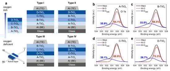
Figure 1.
(a) Schematic device structures of the memristors having four TiOx sub-layers with different oxygen vacancy (Ovac) contents. The stacking sequence of the TiOx sub-layers was varied (types I, II, III, and IV). The thicknesses of the A-TiOx, B-TiOx, C-TiOx, and D-TiOx films were approximately 14.0 nm, 11.5 nm, 11.5 nm, and 9.0 nm, respectively. The O1s spectra measured by using the X-ray photoelectron spectroscopy (XPS) for, (b) A-TiOx, (c) B-TiOx, (d) C-TiOx, and (e) D-TiOx films.
The atomic binding states of TiOx films were analyzed by using X-ray photoelectron spectroscopy (XPS; Thermo Fisher Scientific, Waltham, MA, USA, ESCALAB 250). For the XPS analysis, each TiOx sample was prepared separately. The current-voltage characteristic and the retention characteristics of the memristors were analyzed by using a semiconductor parameter analyzer (Agilent Technologies, Santa Clara, CA, USA, 4155C) which is attached to a probe station in dark ambient condition.
3. Results and Discussion
Figure 1a shows the schematic device structures of the memristors having four TiOx sub-layers with different oxygen vacancy (Ovac) contents. Here, the stacking sequence of the four TiOx sub-layers was varied to find the structure to enhance the resistive switching characteristics of the device (types I, II, III, and IV). The four TiOx sub-layers with different oxygen vacancy contents were fabricated by using different sputtering conditions by varying the gas flow rates of Ar and O2 gases (Ar:O2 = 50:5 sccm, 50:7 sccm, 50:10 sccm and 50:13 sccm). The corresponding TiOx films are designated as A-TiOx, B-TiOx, C-TiOx, and D-TiOx, in the order of decreasing oxygen vacancy content (Figure 1a). Consequently, the A-TiOx film is relatively oxygen-deficient, while the D-TiOx film is relatively oxygen-rich. Also, the thicknesses of A-TiOx, B-TiOx, C-TiOx, and D-TiOx films were approximately 14.0 nm, 11.5 nm, 11.5 nm, and 9.0 nm, respectively. To determine the variation of oxygen vacancy content, an XPS analysis was carried out. Figure 1b–e show the corresponding O1s spectra of the A-TiOx, B-TiOx, C-TiOx, and D-TiOx films, respectively. Here, the fitted curve was deconvoluted to two main peaks centred at around ~530 eV and 531.0~531.5 eV. The peaks at ~530 eV and 531.0–531.5 eV represent the oxygen species in metal–oxygen–metal (M–O–M) and near the oxygen vacancy (O–M–Ovac) [29], respectively. By increasing the PO2, the portion of oxygen vacancy was gradually decreased. For instance, in the case of A-TiOx film, the portion of O–M–Ovac was 35.9%, while it decreased to 33.5%, 30.1%, and 26.7% for the B-TiOx, C-TiOx, and D-TiOx film, respectively.
Since the oxygen vacancy concentration in an oxide film is strongly related to the electrical conductivity of the film [30] and the oxygen vacancies play the key role in the operation of TiOx-based memristors, it is likely that the stacking sequence of oxygen-rich and oxygen-deficient TiOx films would influence the operation of the device. To investigate the effect of multi-layer stacking sequence on the resistive switching characteristics of the memristors, devices having four different stacking sequences were fabricated as schematically shown in Figure 1a. Figure 2a–d show the representative current-voltage (I–V) characteristics of the memristors having the stacking sequences of A-B-C-D (type I), A-C-B-D (type II), A-D-C-B (type III), and A-C-D-B (type IV), respectively. In all cases, the most oxygen-deficient layer, A-TiOx film was placed in the bottom-most part, while the other layers were positioned with different combinations. Here, the TE electrode was set as ground and the bias applied to the BE was swept in the range of −3 V to +3 V to induce the SET and RESET processes. As indicated, the devices with types I, II, and IV stacking sequences showed memristive characteristics, clearly indicating the SET and RESET processes. In the meanwhile, the type III device showed only insulating behaviour without the bistable behaviour. In the case of the type II device (Figure 2b), the device first showed HRS (OFF state) upon sweeping the bias from 0 V to +3 V. Then, at around +2.3 V, transition to the LRS (ON state) starts to occur, which is regarded as the SET process. After reaching +3 V, the LRS maintains, exhibiting the memorizing behaviour. Then, by sweeping the bias to the negative direction, a transition from LRS to HRS occurs at around −2.7 V, which indicates the RESET process. Similar memristive characteristics and switching behaviours were also observed in devices with other stacking sequences such as types I and IV, with slightly different SET and RESET voltages. However, the ION/IOFF ratio was different depending on the device structure. In the tested device structures, the type II device (BE/A-C-B-D/TE) showed the highest ION/IOFF ratio value of ~45 (in average), while, the type I and type IV devices showed ION/IOFF ratio values of ~16 and ~17, respectively. The type III device (BE/A-D-C-B/TE), however, showed no switching behaviour and only insulating I–V characteristics were observed. Figure 2 also shows the I–V data which are repeated for five consecutive cycles. All the devices showed relatively stable I–V behaviour, while the type IV device showed a slight change in the current levels. As shown in Figure 2, during the SET and RESET processes, the current changes gradually, indicating the interface-type mechanism is dominant rather than the filament-type [31]. Concerning the variation of memristive behavior by the stacking sequence, we expect that the supply and migration of oxygen vacancies from the underneath TiOx sub-layers to the TE/top-TiOx interface are important [31]. In our results, the type I, II, and IV devices showed the memristive behaviour while the type III device showed insulating characteristics. In particular, in the cases of types I and II, the most oxygen-rich TiOx layer (D-TiOx) with the lowest concentration of oxygen vacancies is placed on the top-most layer, contacting the TE, while the relatively oxygen-deficient TiOx layers with larger concentrations of oxygen vacancies are placed underneath. Therefore, during the SET process, these relatively oxygen-deficient TiOx layers can efficiently supply the oxygen vacancies and can contribute to the interface-type resistive switching behaviour. Comparing the type I and II devices, the positions of B- and C-TiOx layers are different, where in type II, the second-most oxygen-deficient TiOx layer (B-TiOx) is placed beneath the top D-TiOx layer. Therefore, compared to type I device, more oxygen vacancies can be supplied to the top D-TiOx layer, allowing larger resistive variation during switching. In the cases of types III and IV, the most oxygen-rich D-TiOx layer is placed in the middle parts of the stacking. Therefore, the supply of oxygen vacancies towards the TE/top-TiOx interface can be relatively smaller compared to type I and II devices. Also, considering that the oxygen vacancies migrate toward the TE/top-TiOx interface during the SET process, the decrease of resistance in the D-TiOx layer can be higher in type IV device compared to type III.
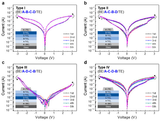
Figure 2.
The representative current–voltage (I–V) characteristics of memristors having the stacking sequences of (a) A-B-C-D (type I), (b) A-C-B-D (type II), (c) A-D-C-B (type III), and (d) A-C-D-B (type IV), respectively. The top electrode (TE) was set as ground and the bias applied to the bottom electrode (BE) was swept in the sequence of 0 V → +3 V → −3 V → 0 V. The measurement was repeated five times in each case.
The data retention characteristics of memristors are important for realizing highly stable memory devices as well as neuromorphic or synaptic devices. Figure 3a shows the data retention characteristics of type I, II, and IV devices. Here, the LRS and HRS states were programmed with pulsed biases of +3 V and −3 V, respectively (pulse widths of 100 ms). Also, the programmed states were read for an interval of 200 s up to 10,000 s, with a read voltage of +1 V. As displayed, devices with types I, II, and IV showed stable operation up to 10,000 s without a considerable change in the current levels of ON (ION) and OFF (IOFF) states. Therefore, the ION/IOFF ratios are maintained correspondingly as shown in Figure 3b. Among the tested devices, the type II memristors exhibited the highest ION/IOFF ratio, while the type I memristor showed the lowest ION/IOFF ratio. Nonetheless, the results indicate that regardless of the stacking sequence, the TiOx-based memristors showed relatively stable operations.
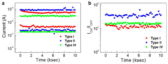
Figure 3.
(a) The data retention characteristics of TiOx-based memristors (type I, II, and IV). The ON and OFF states were programmed with biases of +3 V and −3 V, respectively. Also, the read voltage was +1 V. (b) The variation of ION/IOFF ratio during the data retention test up to 10 ks.
Symmetric synaptic weight update characteristics between long-term potentiation (LTP) and long-term depression (LTD) is a crucial factor in designing synaptic devices that directly affects learning accuracy of neuromorphic computing [32,33]. As shown in Figure 4, we measured the long-term plasticity of the type II device by applying a pulse train consisting of potentiation (VPOT), depression (VDEP) and read pulses. The VPOT was fixed at +2 V during the potentiation process while the VDEP was varied as −1 V and −2 V as shown in Figure 4a (“A” pulse train) and b (“B” pulse train), respectively. Each potentiation and depression was performed for 300 cycles each. The duration time of each pulse was 50 ms and the pulse interval was ~1.45 s (see the inset of Figure 4 showing the pulse train of the three cycles). As shown in Figure 4, bidirectional switching behaviour was obtained in which the channel conductance was set to various conducting states between 0.136 μS and 2.02 μS for both conductance rise and fall processes. The acquired channel conductance represents a non-volatile behaviour. Thus, increasing and decreasing the channel conductance can be regarded as synaptic LTP and LTD, respectively. In addition to the symmetry, the change in linear conductance between LTP and LTD processes is also an important factor [32,33]. So, we calculated the nonlinearity values between LTP and LTD processes through the potentiation and depression data. The nonlinearity factors (α) were extracted from the characteristic curves shown in Figure 4. We use the device behavioural model [34], where the conductance change is represented with the following equations [34]:
where, P is number of pulses, B is a fitting parameter, A is the nonlinearity of potentiation () and depression (), GLTP and GLTD are the conductance for LTP and LTD, and Gmax, Gmin and Pmax are the experimental data which represent the maximum conductance, minimum conductance and the maximum number of pulses required to change the device states between minimum and maximum conductance. The non-linearity values for “A” pulse train were = 2.4 and = −4.6 for the potentiation and depression, respectively (Figure 4a). The non-linearity values for “B” pulse train were = 2.2 and = −8.74 (Figure 4b).
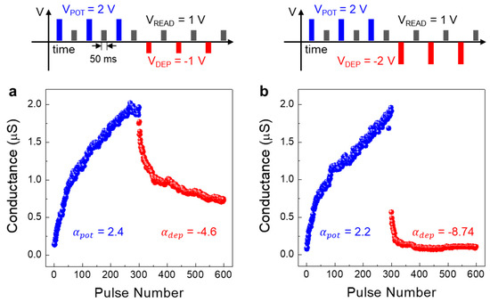
Figure 4.
The weight update characteristics (conductance vs. number of pulse) of memristors with different depression pulse voltage (a) “A” pulse train condition (VPOT = +2 V, VDEP = −1 V), and (b) “B” pulse train condition (VPOT = +2 V, VDEP = −2 V).
Using the “NeuroSim+” platform, a supervised artificial neural network learning simulation of the MNIST handwritten recognition data set was performed by applying the non-linearity, conductance level, and the cycle-to-cycle variation of our device [34,35]. In the simulation, we used a three-layer neural network with 400 pre-neurons, 100 hidden neurons and 10 output neurons which correspond to 10 classes of digits (0–9). The detail of the three-layer multilayer perceptron network is shown in Figure 5a [36]. The TiOx multi-layer memristor acts as a memory element in a crossbar array and their memristor conductivity change was used as the weight update to run the back-propagation algorithm. Here, the crossbar is considered as part of a “neuron core” that executes vector-matrix multiplication (inference) and outer-product updates (learning) operations [37]. The sum of the input neuron signal vector and the first layer of the synaptic weight is transferred to the input vector of the hidden layer after activation and binarization [9]. For each epoch, 60,000 training data set were used for training, and accuracy was obtained using a 10,000 test data set.
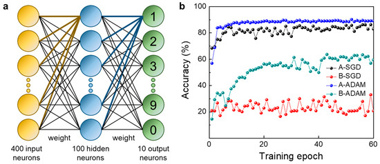
Figure 5.
(a) A three-layer perceptron-based artificial neural network for Modified National Institute of Standards and Technology (MNIST) handwritten recognition, and (b) the accuracy with training epochs based on two pulse conditions and two algorithms which were stochastic gradient descent (SGD) and adaptive moment estimation (ADAM).
By using algorithmic methods which was stochastic gradient descent (SGD) and adaptive moment estimation (ADAM) weight update, the accuracy of MNIST handwritten recognition was obtained. As shown in Figure 5b, in the case of the “A” pulse train condition (VPOT = +2 V, VDEP = −1 V), the accuracy was 82.99% when using the SGD, and 89.18% when using the ADAM. On the other hand, in the case of ‘B’ pulse train condition (VPOT = +2 V, VDEP = −2 V), the accuracy was 20.80% when using the SGD, and 59.52% when using the ADAM. Because the LTD non-linearity value of the “A” pulse train condition is smaller compared to that of the “B” pulse train condition, it is advantageous for learning process which resulted in a higher accuracy. The learning algorithm also plays an important role in accuracy. The SGD method calculates an error from the current weight, predicting a direction in which the weight should change, and learns at a predetermined step size. However, the ADAM method stored the exponential average of the slopes calculated so far to modulate the weight direction, and also stored the exponent average of the squared slopes to set the step size [38,39]. Thus, when using the ADAM method, there were more data to store, but accurate learning could be achieved using our device.
4. Conclusions
In this paper, we demonstrated the multi-layer TiOx memristors for potential memory and neuromorphic applications. The four TiOx sub-layers with different oxygen vacancy content were fabricated by using different sputtering conditions by varying the gas flow rates of Ar and O2. Also, through the XPS analysis, the ratio of M–O–M and M–Ovac of oxygen peaks at different gas flow conditions was determined. By comparing the memristor characteristics according to the stacking sequence of the memristor device with a multi-layer structure, it was confirmed that the ION/IOFF ratio value is the highest as 45 in the type II stacking sequence structure. Also, by measuring the retention time in the on state and off state, it was confirmed that the current is maintained without degradation over 10,000 s. In addition, the long-term plasticity (LTP/LTD) was measured for the type II stacking sequence structure to obtain LTP and LTD non-linearity according to different depression voltage pulses. Two depression pulse voltage conditions and algorithm methods (SGD and ADAM) were used, and the highest accuracy of 89.18% was obtained when VDEP = −1 V and with the ADAM algorithm.
Author Contributions
M.K. and K.Y. performed the experiments and the data analysis; S.-P.J., S.K.P. and Y.-H.K. contributed to draft the manuscript and carry-out the data analysis and evaluation. S.K.P. and Y.-H.K. made the substantial contribution to the concept of experiments and was responsible for leading the project. All authors read and approved the final manuscript.
Funding
This research was partially supported by the National Research Foundation of Korea (NRF) grant funded by the Korea government (MSIP) (No. NRF-2019M3F3A1A02071601), and the Chung-Ang University Research Scholarship Grants in 2018.
Conflicts of Interest
The authors declare no conflict of interest.
References
- Sun, W.; Gao, B.; Chi, M.; Xia, Q.; Yang, J.J.; Qian, H.; Wu, H. Understanding memristive switching via in situ characterization and device modeling. Nat. Commun. 2019, 10, 1–13. [Google Scholar] [CrossRef] [PubMed]
- Bayat, F.M.; Prezioso, M.; Chakrabarti, B.; Nili, H.; Kataeva, I.; Strukov, D. Implementation of multilayer perceptron network with highly uniform passive memristive crossbar circuits. Nat. Commun. 2018, 9, 1–7. [Google Scholar] [CrossRef] [PubMed]
- Mikhaylov, A.N.; Morozov, O.A.; Ovchinnikov, P.E.; Antonov, I.N.; Belov, A.I.; Korolev, D.S.; Sharapov, A.N.; Gryaznov, E.G.; Gorshkov, O.N.; Pigareva, Y.I. One-board design and simulation of double-layer perceptron based on metal-oxide memristive nanostructures. IEEE Trans. Emerg. Topics Comput. 2018, 2, 371–379. [Google Scholar] [CrossRef]
- Cai, F.; Correll, J.M.; Lee, S.H.; Lim, Y.; Bothra, V.; Zhang, Z.; Flynn, M.P.; Lu, W.D. A fully integrated reprogrammable memristor–CMOS system for efficient multiply–accumulate operations. Nat. Electron. 2019, 2, 290–299. [Google Scholar] [CrossRef]
- Mehonic, A.; Cueff, S.; Wojdak, M.; Hudziak, S.; Jambois, O.; Labbé, C.; Garrido, B.; Rizk, R.; Kenyon, A.J. Resistive switching in silicon suboxide films. J. Appl. Phys. 2012, 111, 074507. [Google Scholar] [CrossRef]
- Mikhaylov, A.N.; Belov, A.I.; Guseinov, D.V.; Korolev, D.S.; Antonov, I.N.; Efimovykh, D.V.; Tikhov, S.V.; Kasatkin, A.P.; Gorshkov, O.N.; Tetelbaum, D.I. Bipolar resistive switching and charge transport in silicon oxide memristor. Mater. Sci. Eng. B 2015, 194, 48–54. [Google Scholar] [CrossRef]
- Wong, H.P.; Lee, H.; Yu, S.; Chen, Y.; Wu, Y.; Chen, P.; Lee, B.; Chen, F.T.; Tsai, M. Metal–Oxide RRAM. Proc. IEEE 2012, 100, 1951–1970. [Google Scholar] [CrossRef]
- Wang, Z.; Joshi, S.; Savel’ev, S.E.; Jiang, H.; Midya, R.; Lin, P.; Hu, M.; Ge, N.; Strachan, J.P.; Li, Z.; et al. Memristors with diffusive dynamics as synaptic emulators for neuromorphic computing. Nat. Mater. 2017, 16, 101–108. [Google Scholar] [CrossRef]
- Choi, S.; Tan, S.H.; Li, Z.; Kim, Y.; Choi, C.; Chen, P.-Y.; Yeon, H.; Yu, S.; Kim, J. SiGe epitaxial memory for neuromorphic computing with reproducible high performance based on engineered dislocations. Nat. Mater. 2018, 17, 335–340. [Google Scholar] [CrossRef]
- Chua, L. Memristor-The missing circuit element. IEEE Trans. Circuit Theory 1971, 18, 507–519. [Google Scholar] [CrossRef]
- The Memristor Revisited. Available online: https://www.nature.com/articles/s41928-018-0083-3 (accessed on 3 January 2020).
- He, W.; Sun, H.; Zhou, Y.; Lu, K.; Xue, K.; Miao, X. Customized binary and multi-level HfO2−x-based memristors tuned by oxidation conditions. Sci. Rep. 2017, 7, 10070. [Google Scholar] [CrossRef]
- Kumar, S.; Strachan, J.P.; Williams, R.S. Chaotic dynamics in nanoscale NbO2 Mott memristors for analogue computing. Nature 2017, 548, 318–321. [Google Scholar] [CrossRef] [PubMed]
- Kim, W.; Chattopadhyay, A.; Siemon, A.; Linn, E.; Waser, R.; Rana, V. Multistate Memristive Tantalum Oxide Devices for Ternary Arithmetic. Sci. Rep. 2016, 6, 36652. [Google Scholar] [CrossRef] [PubMed]
- Barnes, B.K.; Das, K.S. Resistance Switching and Memristive Hysteresis in Visible-Light-Activated Adsorbed ZnO Thin Films. Sci. Rep. 2018, 8, 2184. [Google Scholar] [CrossRef] [PubMed]
- Salaoru, I.; Prodromakis, T.; Khiat, A.; Toumazou, C. Resistive switching of oxygen enhanced TiO2 thin-film devices. Appl. Phys. Lett. 2013, 102, 013506. [Google Scholar] [CrossRef]
- Zaffora, A.; Macaluso, R.; Habazaki, H.; Valov, I.; Santamaria, M. Electrochemically prepared oxides for resistive switching devices. Electrochim. Acta 2018, 274, 103–111. [Google Scholar] [CrossRef]
- Aglieri, V.; Zaffora, A.; Lullo, G.; Santamaria, M.; Di Franco, F.; Lo Cicero, U.; Mosca, M.; Macaluso, R. Resistive switching in microscale anodic titanium dioxide-based memristors. Superlattices Microstruct. 2018, 113, 135–142. [Google Scholar] [CrossRef]
- Bousoulas, P.; Michelakaki, I.; Tsoukalas, D. Influence of Ti top electrode thickness on the resistive switching properties of forming free and self-rectified TiO2−x thin films. Thin Solid Films 2014, 571, 23–31. [Google Scholar] [CrossRef]
- Strukov, D.B.; Snider, G.S.; Stewart, D.R.; Williams, R.S. The missing memristor found. Nature 2008, 453, 80–83. [Google Scholar] [CrossRef]
- Li, D.; Li, M.; Zahid, F.; Wang, J.; Guo, H. Oxygen vacancy filament formation in TiO2: A kinetic Monte Carlo study. J. Appl. Phys. 2012, 112, 073512. [Google Scholar] [CrossRef]
- Carta, D.; Salaoru, I.; Khiat, A.; Regoutz, A.; Mitterbauer, C.; Harrison, N.M.; Prodromakis, T. Investigation of the Switching Mechanism in TiO2-Based RRAM: A Two-Dimensional EDX Approach. ACS Appl. Mater. Interfaces 2016, 8, 19605–19611. [Google Scholar] [CrossRef]
- Sadi, T.; Mehonic, A.; Montesi, L.; Buckwell, M.; Kenyon, A.; Asenov, A. Investigation of resistance switching in SiOxRRAM cells using a 3D multi-scale kinetic Monte Carlo simulator. J. Phys. Condens. Matter 2018, 30, 084005. [Google Scholar] [CrossRef] [PubMed]
- Guseinov, D.; Korolev, D.; Belov, A.; Okulich, E.; Okulich, V.; Tetelbaum, D.; Mikhaylov, A. Flexible Monte-Carlo approach to simulate electroforming and resistive switching in filamentary metal-oxide memristive devices. Model. Simul. Mater. Sci. Eng. 2019, 28, 015007. [Google Scholar] [CrossRef]
- Dash, C.S.; Sahoo, S.; Prabaharan, S.R.S. Resistive switching and impedance characteristics of M/TiO2−x/TiO2/M nano-ionic memristor. Solid State Ionics 2018, 324, 218–225. [Google Scholar] [CrossRef]
- Zhang, H.; Ju, X.; Yew, K.S.; Ang, D.S. Implementation of Simple but Powerful Trilayer Oxide-Based Artificial Synapses with a Tailored Bio-Synapse-Like Structure. ACS Appl. Mater. Interfaces 2020, 12, 1036–1045. [Google Scholar] [CrossRef] [PubMed]
- Li, Y.; Li, X.; Fu, L.; Chen, R.; Wang, H.; Gao, X. Effect of interface layer engineering on resistive switching characteristics of ZrO 2-based resistive switching devices. IEEE Trans. Electron Devices 2018, 65, 5390–5394. [Google Scholar] [CrossRef]
- Wu, W.; Wu, H.; Gao, B.; Deng, N.; Qian, H. Suppress variations of analog resistive memory for neuromorphic computing by localizing Vo formation. J. Appl. Phys. 2018, 124, 152108. [Google Scholar] [CrossRef]
- Skaja, K.; Andrä, M.; Rana, V.; Waser, R.; Dittmann, R.; Baeumer, C. Reduction of the forming voltage through tailored oxygen non-stoichiometry in tantalum oxide ReRAM devices. Sci. Rep. 2018, 8, 10861. [Google Scholar] [CrossRef]
- Gross, M.; Winnacker, A.; Wellmann, P.J. Electrical, optical and morphological properties of nanoparticle indium–tin–oxide layers. Thin Solid Films 2007, 515, 8567–8572. [Google Scholar] [CrossRef]
- Sawa, A. Resistive switching in transition metal oxides. Mater. Today 2008, 11, 28–36. [Google Scholar] [CrossRef]
- Jang, J.; Park, S.; Burr, G.W.; Hwang, H.; Jeong, Y. Optimization of Conductance Change in Pr1–xCaxMnO3-Based Synaptic Devices for Neuromorphic Systems. IEEE Electron Device Lett. 2015, 36, 457–459. [Google Scholar] [CrossRef]
- Wang, I.T.; Chang, C.-C.; Chiu, L.-W.; Chou, T.; Hou, T.-H. 3D Ta/TaOx/TiO2/Ti synaptic array and linearity tuning of weight update for hardware neural network applications. Nanotechnology 2016, 27, 365204. [Google Scholar] [CrossRef]
- Chen, P.; Peng, X.; Yu, S. NeuroSim+: An integrated device-to-algorithm framework for benchmarking synaptic devices and array architectures. In Proceedings of the IEEE International Electron Devices Meeting (IEDM), San Francisco, CA, USA, 2–6 December 2017. [Google Scholar]
- LeCun, Y.; Bottou, L.; Bengio, Y.; Haffner, P. Gradient-based learning applied to document recognition. Proc. IEEE 1998, 86, 2278–2323. [Google Scholar] [CrossRef]
- Kataeva, I.; Merrikh-Bayat, F.; Zamanidoost, E.; Strukov, D. Efficient training algorithms for neural networks based on memristive crossbar circuits. In Proceedings of the International Joint Conference on Neural Networks (IJCNN), Killarney, Ireland, 12–17 July 2015; pp. 1–8. [Google Scholar]
- Yang, C.-S.; Shang, D.-S.; Liu, N.; Fuller, E.J.; Agrawal, S.; Talin, A.A.; Li, Y.-Q.; Shen, B.-G.; Sun, Y. All-Solid-State Synaptic Transistor with Ultralow Conductance for Neuromorphic Computing. Adv. Funct. Mater. 2018, 28, 1804170. [Google Scholar] [CrossRef]
- Darken, C.; Chang, J.; Moody, J. Learning rate schedules for faster stochastic gradient search. In Proceedings of the 1992 IEEE Workshop Neural Networks for Signal Processing II, Helsingoer, Denmark, 31 August–2 September 1992; pp. 3–12. [Google Scholar]
- Kingma, D.P.; Ba, J. Adam: A method for stochastic optimization. In Proceedings of the International Conference on Learning Representations, San Diego, CA, USA, 7 May 2015. [Google Scholar]


© 2020 by the authors. Licensee MDPI, Basel, Switzerland. This article is an open access article distributed under the terms and conditions of the Creative Commons Attribution (CC BY) license (http://creativecommons.org/licenses/by/4.0/).