Article

Deep Reactive Ion Etching of Z-Cut Alpha Quartz for MEMS Resonant Devices Fabrication

State Key Laboratory for Manufacturing System Engineering, Xi’an Jiaotong University, Xi’an 710049, China
*
Author to whom correspondence should be addressed.
Micromachines 2020, 11(8), 724; https://doi.org/10.3390/mi11080724
Submission received: 15 July 2020 / Revised: 20 July 2020 / Accepted: 23 July 2020 / Published: 26 July 2020
(This article belongs to the Special Issue Micro-Manufacturing and Applications)

Abstract

:
Quartz is widely used in microelectromechanical systems (MEMS). Especially, MEMS quartz resonators are applied to sensors and serve as sensitive elements. The capability of deep etching is a limitation for the application. Presented in this paper is a deep and high accuracy reactive ion etching method applied to a quartz resonator etching process with a Cr mask. In order to enhance the capability of deep etching and machining accuracy, three kinds of etching gas (C4F8/Ar, SF6/Ar and SF6/C4F8/Ar), bias power, inductively coupled plasma (ICP) power and chamber pressure were studied in an industrial reactive ion etching machine (GDE C200). Results indicated that the SF6/C4F8/Ar chemistry gas is the suitable and optimal choice. Experiment results indicate that Cr (chromium) mask can obtain a higher selectivity than aluminum and titanium mask. A “sandwich” structure composed of Al layer-Cr layer-Al layer-Cr layer was proposed. The Al (aluminum) film can play the role of releasing stress and protecting gold electrodes, which can enhance the thickness of metal mask. An optimized process using SF6/C4F8/Ar plasmas showed the quartz etching rate of 450 nm/min. Meanwhile, a microchannel with a depth of 75.4 µm is fabricated, and a nearly vertical sidewall profile, smooth surface is achieved.

1. Introduction

Quartz has been widely used as a resonator material in micro-sensors [1,2,3] due to its excellent material properties such as its high quality factor [4,5,6,7,8,9,10], high frequency stability and inherent piezoelectric characteristics. A major obstacle limiting the wide use of quartz is that there exists a limited variety of suitable processing methods for producing structures with desired shapes. In order to solve this problem, a conventional method known as wet chemical etching has been studied by several researchers [1,11,12,13], which is mainly performed in aqueous hydrofluoric (HF), and often in combination with ammonium fluoride (NH4F) as a buffer. However, the high degree of anisotropy, the trigonal symmetry of the quartz crystal and large etch rate hinder its study and use. Recently, a few micromachining processes such as laser beam machining (LBM) [14], abrasive jet machining (AJM) [15,16] and electrochemical discharge machining (ECDM) [17,18,19,20,21] have been studied for realizing micro-structures on quartz substrate. Though the etching rate is overtly improved with these technologies, it is not suitable for manufacturing complex structures and mass production. Moreover, the laser energy results in a quartz crystal denaturation at the edge of the resonant beam in LBM technology; the roughness and flatness of the etched bottom and sidewall cannot achieve the accuracy requirements of the resonator in LBM and ECDM technology, which induces an undesirable effect on the performance of quartz resonators. Moreover, the machining accuracy is too low to manufacture much smaller micro-resonators. Therefore, a deep dry etching method with inductively coupled plasma has been investigated to obtain an excepted profile [4,5,9,22,23,24,25,26,27,28,29,30,31,32,33,34,35,36].
Several typical masks, such as metal masks, photoresist masks and metallic compound masks have been discussed so far [24,28,34,35,36,37,38,39,40,41,42,43]. It is known that the deep and high etching rate of glasses is not feasible with standard photoresist masks due to low selectivity and mask profile degradation during the prolonged process [37,38]. Therefore, other masks have drawn much attention in recent years. A thin sputtered Al2O3 (aluminum oxide) mask was studied to achieve high selectivity to SiO2 (silicon dioxide) when the gas composition of the C4F8/SF6 mixture, pressure, and bias power was properly tuned [28,38]. However, the original thickness of Al2O3 was 100 nm with a 20 min deposition process. It was therefore infeasible to acquire a deep etching depth due to the disadvantage of slow sputtering and deposition rate. Moreover, a novel process was designed by periodically oxidizing the surface of an Al mask in oxygen plasma to obtain an Al2O3 mask during the breaks of the SiO2 etching process [29,44]. Thus, 5 μm thick silica waveguides were achieved with vertical and smooth profiles using an initial Al mask of only 100 nm. However, the extra oxidizing step resulted in the etching duration increasing and the throughput suffered considerably. In order to achieve a deep etching of SiO2, the trade-off between the selectivity and thickness of the mask should be paid attention to.
Owing to the high deposition rate and acceptable selectivity, Cr and Ni were selected as a hard mask for the deep dry etching of SiO2. A 27 μm-deep trench has been achieved with a 15 μm Ni hard mask [24], using SF6 and SF6 /Ar plasmas in an inductively coupled plasma (ICP) reactor. However, the angle and roughness of sidewalls were unsatisfactory, which is an obstacle to using this approach to manufacture resonators. Under optimized etching conditions, deep trench etching of borosilicate glass to a 32 μm depth using an electroplated Cr mask created by wet etching was reported [24]. Nevertheless, the etching depth was less than that required for the quartz resonator. Meanwhile, some investigators have explored the AlN (Aluminum nitride) hard mask to receive a higher selectivity possibility [22,28,34,38]. However, most of the studies concentrate on only one aspect to obtain high selectivity but neglect others. Consequently, more research on improving etching depth and gaining high quality surface profiles should be focused on.
In light of the above research studies, it should be noted that the presented results of SiO2 etching process development were performed with amorphous silicon oxide, such as undoped silicon oxide glass (USG), silica, fused quartz and quartz glass. In reality, the material of an electromechanical resonator is the single crystal quartz [13,45,46,47], which is selected due to its piezoelectric characteristic with low-loss elastic and electrical characteristics. Although the chemical composition of the above-mentioned materials is the same, and the deep dry-etching distinctions of them are in existence, more attention should be paid to the deep quartz etch. However, information and investigations on deep dry etching on single crystal quartz substrate for quartz resonators fabrication are scarce so far. Owing to the anisotropic property of alpha quartz, the basic plasma etching process parameters of single crystal quartz are more complex in comparison with those of amorphous silicon oxide. In this case, a systematic research on the deep dry etching of anisotropic single crystal quartz is required, especially the Z-cut alpha quartz. Thus, in this work, we investigate the possibilities for the deep dry etching of the Z-cut alpha quartz crystal with metal masks. The preparation of the thick Cr mask is investigated and a “sandwich” structure is proposed to reduce the residual stress. Additionally, in order to obtain a smooth etched surface and vertical sidewall, the etching process parameters are optimized and tuned; a MEMS quartz resonant sensor is fabricated through the proposed etching technology.

2. Experiment

The Z-cut alpha quartz etching process was performed in a deep reactive ion etching (DRIE) system (GDE C200, China, Beijing), which has two high-density 13.56 MHz plasma sources (inductively coupled plasma (ICP) and capacitive coupled plasma (CCP), designed to etch materials which are infeasible to etch using conventional reactive ion etching (RIE) or ICP sources, such as silicon oxide, silicon nitride, aluminum oxide. The ICP source was a planar electrode on the top of the reaction chamber with a spiral coil. The ICP energy was supplied by electromagnetic inductions with a frequency of 13.56 MHz. The CCP source had the same frequency and was placed at the bottom of the reaction chamber. The cooled chuck with electrostatic clamping and helium backside cooling was served as a stage in which the target wafer was kept. The internal diameter of the reactor was 500 mm and the distance from the substrate chuck to the top of the reaction chamber was 150 mm. In this system the ICP produced the plasma of ions, while the CCP was applied to accelerate the ions onto the cathode. In order to guarantee the stability of the etching process, a chiller was employed to maintain the chuck at pre-set temperature.
In order to enable a high quality of the deposited Cr layer, etching targets, and z-cut alpha quartz wafers were subjected to mechanical cleaning through a mixture solution of concentrated sulfuric acid and hydrogen peroxide at 80 °C. Three types of metal hard masks were evaluated in our research. The metal masks were deposited by magnetron sputtering in a multi-cathode sputter deposition platform system (DENTON, DISCOVERY635, Denton, TX, USA). Before the metal layer was created, a photoresist (AZ4620, RDMICRO, SuZhou, China) with a thickness of about 13 μm was spin-coated on the quartz wafer and patterned by photolithography. Then, a subsequent lift-off was applied to stripping the photoresist.
The length, width and thickness of the quartz wafer (LINDE, Xi’an, China) was 34.5 mm, 29.5 mm and 100 µm, respectively. The diameter of the wafer chuck was 4 inches. Thus, the quartz wafer was fixed on a silicon wafer with perfluoropolyether during the etching process. The wafer chuck temperature was 90 °C. Three etching gas mixtures (C4F8/Ar, SF6/Ar and C4F8/SF6/Ar), bias power, ICP power and chamber pressure were studied in our experiment. Prior to etching, residual debris and organic contaminants were removed from the surface of the wafers with dry nitrogen gas and oxygen plasma, respectively.

3. Results

3.1. Effect of Etching Gas

Three gas mixtures (C4F8/Ar, SF6/Ar and SF6/SF4/Ar) were investigated with a Cr mask in this paper. The initial set of etching parameters: coil (ICP) power 1600 W, platen (bias) power 200 W, pressure 5 mT, and total gas flow rate fixed at 110 sccm. All gas percentages are in volume. The main challenge of deep quartz etching is in the production of high-energy ions to break the strong Si–O bonds while maintaining acceptable selectivity towards the mask material and vertical profile. Ar gas served as a bombardment component, it enhanced the sputtering component of the etching which led to an increased quartz etching rate. However, the etching selectivity was found to be slightly reduced, possibly because of the increased bombardment rate of the Cr mask at the same time.

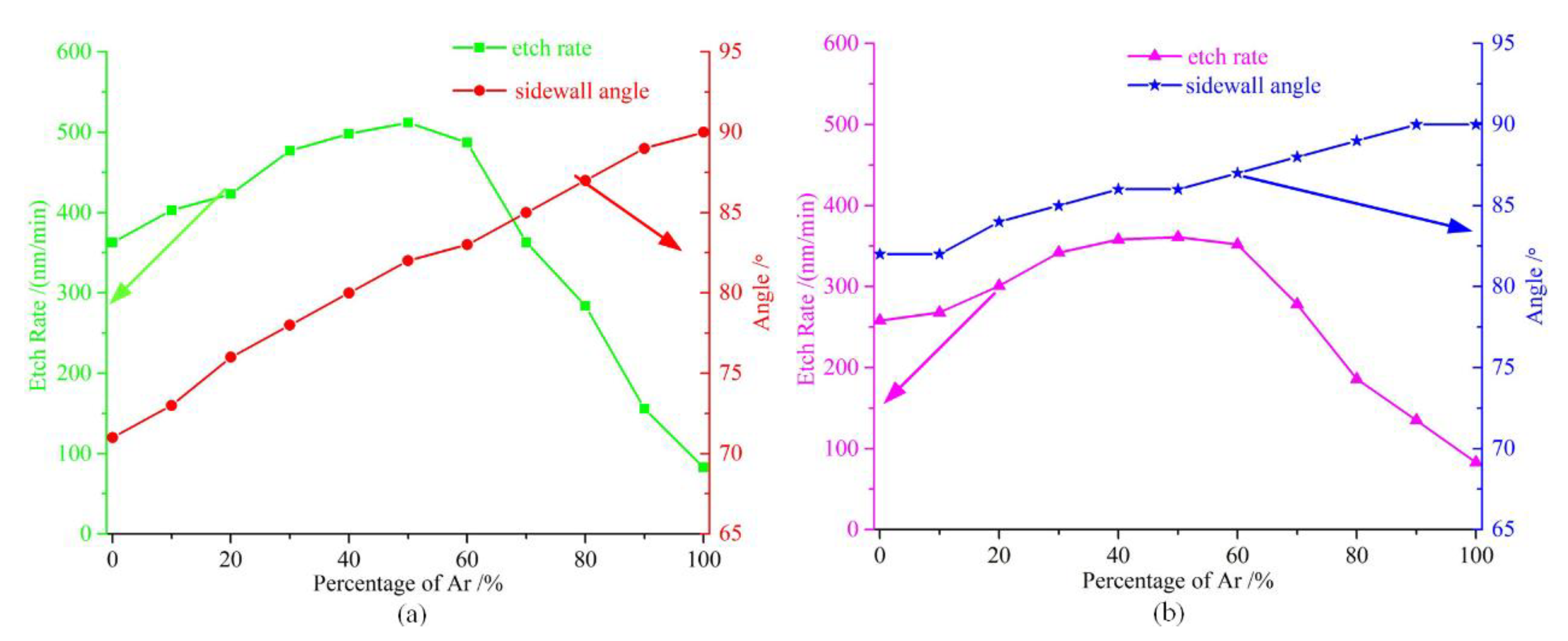
3.1.1. Mixture of C4F8/Ar and SF6/Ar

Figure 1a shows the dependence of the quartz etching rate and sidewall angle with a Cr mask versus the C4F8 percentage in the mixture with Ar. The C4F8 flow ratio ranged from 0% to 100%. It can be seen that the reduction in the C4F8 percentage resulted in an improvement in the sidewall angle. However, when the C4F8 flow ratio was less than 50%, the etching rate increased with the C4F8 percentage increasing due to the insufficiency of the radicals. Moreover, with a high percentage of C4F8 in the total flow rate, most of the reactive gases were radicals, which resulted in the etching rate keeping at a high level. Furtermore, the increasing C4F8 flow ratio resulted in an increase in the passivating neutral-to-ion flux ratio leading to a more tapered profile due to the increasing re-deposition of C-rich by-products on the sidewalls, as explained by Bliznetsov in 2015 [22]. To ensure that the gas mixture has sufficient reactive etchants and to keep the etched sidewall profile at an approximate vertical position, it is better to keep the C4F8 flow ratio within the range of 40~70%.
In order to avoid influence by the C-rich by-products, SF6 was introduced along with Ar to determine its effect on the deep quartz etching. As Figure 1b shows, it can be observed that the mixture of SF6 and Ar led to an improvement of the sidewall angle, because of the disappearing of the re-deposition by-products. Furthermore, the increasing of the SF6 flow rate resulted in a slower reduction in the sidewall angle than that of C4F8. However, it was evident that the etching rate was significantly lower in contrast to C4F8, probably because the ion energies and numbers of SF6 were less than that of C4F8 at same flow rate. Thus, it is conducive to the improvement of the sidewall profile by adding SF6 into the gas chemistry in the deep quartz etching process. Furthermore, the increasing SF6 levels lead to a deterioration of the sidewall angle, which probably results from the increasing of sulfur content.

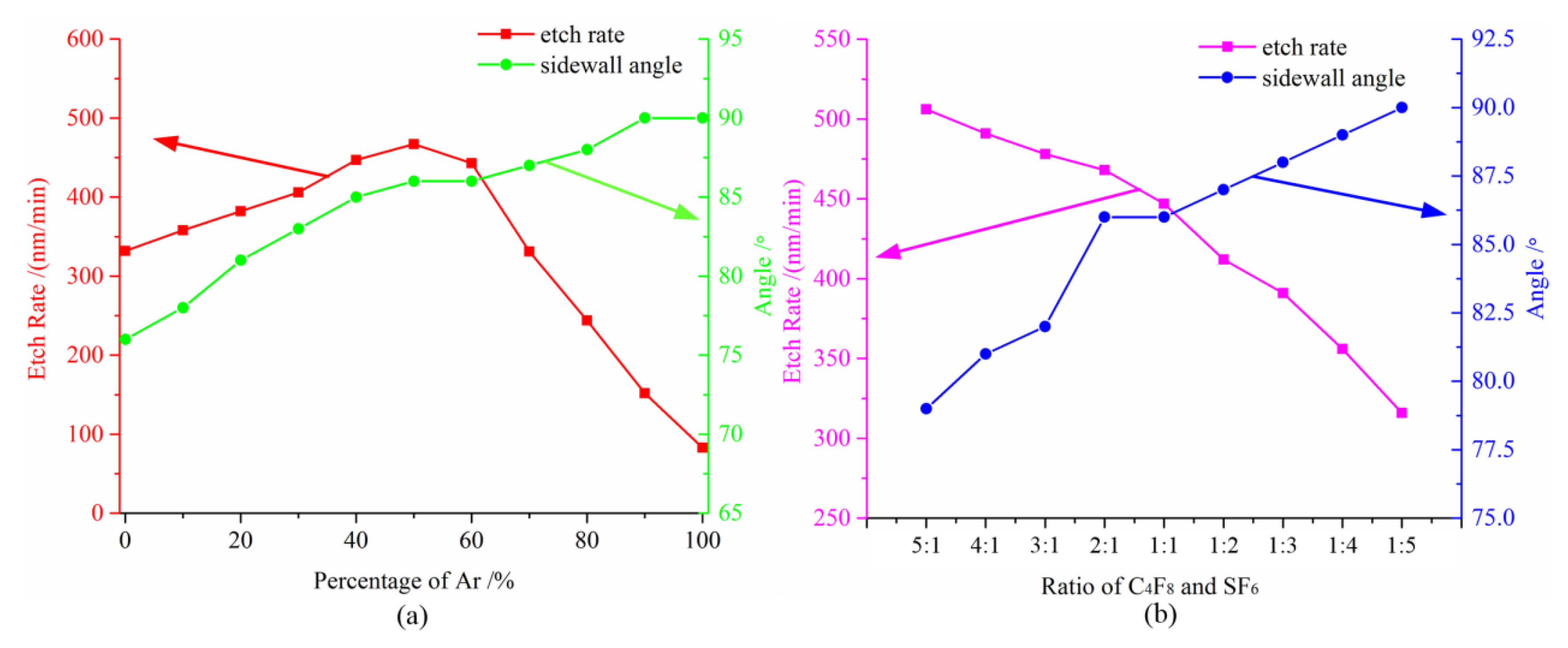
3.1.2. Mixture of C4F8/ SF6/Ar

From the above experiments it is clear that the combination of C4F8/Ar or SF6/Ar is not the optimal decision to achieve deep quartz etching. Thus, a combination of C4F8, SF6 and Ar was selected as the etching media. Figure 2a shows the etching rates of the quartz as a function of the percentage of the Ar flow rate to the total flow rate (Ar + reactive gases). It is obvious that the etching rate is improved. In addition, the Ar flow ratio was kept at 50%, a nearly vertical (87°) sidewall profile was produced. Compared to C4F8/Ar, it can be seen that the sidewall profile is improved with no deterioration in the etching rate. Compared to SF6/Ar, it is obvious that the etching rate is improved significantly. The sidewall profile is acceptable when the percentage of Ar is higher than 50%. In other words, the three-gas mixture is conducive to improving the etching process technology.
A further study was implemented by changing the rate of C4F8 and SF6, in order to investigate the effect of the carbon content. Results for the etch rate and sidewall angle versus the rate of C4F8 and SF6 in the mixture for quartz wafers are presented in Figure 2b (the percentage of Ar was kept at 50%). It is seen that when the rate of C4F8 and SF6 changes from 5:1 to 1:5, the etching rate decreases by almost two-fold. In comparison, the verticality of profile increases to 89.8°. This result indicates that the percentage of the C4F8 flow rate has an optimal range in the total flow rate. In conclusion, to ensure that, the rate of the three chemical gases (C4F8/SF6/Ar) should be approximately maintained at 1:1:2, which can keep the etched sidewall profile at a vertical position. Additionally, an acceptable etching rate also can be obtained in this etching process. Thus, compared to C4F8/Ar and SF6/Ar, the mixture of the C4F8/SF6/Ar process provided both a better etching rate and less by-product re-deposition on the sidewalls. Therefore, we continued the C4F8/SF6/Ar process optimization.

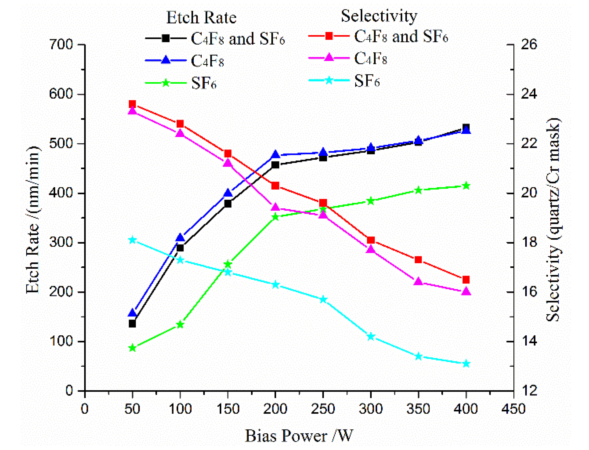
3.2. Effect of Bias Power

The energy of the bombardment component depends on the bias power, which has an effect on the etching rate and selectivity. A test was carried out to investigate the influence on the etching rate and selectivity induced by the bias power. Figure 3 presents the quartz etching rate and selectivity versus bias power. With the decrease in bias power, it is seen that the selectivity drastically improved, and the etch rate dropped. When the bias power changed from 50 W to 400 W, the etch rates increased to 532 nm/min. This result indicates that the bias power has a direct influence on etching efficiency. However, the selectivity for Cr mask declined 46.5% at the same case.
In addition, high bias power resulted in a micro-trench at the position between the sidewall and the bottom surface, as shown in Figure 4. Furthermore, when bias power is the excessive high, the etching bottom is rough as shown in Figure 5, which results from the bombardment with much high energy. Thus, to strike a balance between selectivity and etch rate, an appropriate bias power should be chosen for the deep quartz etching process.

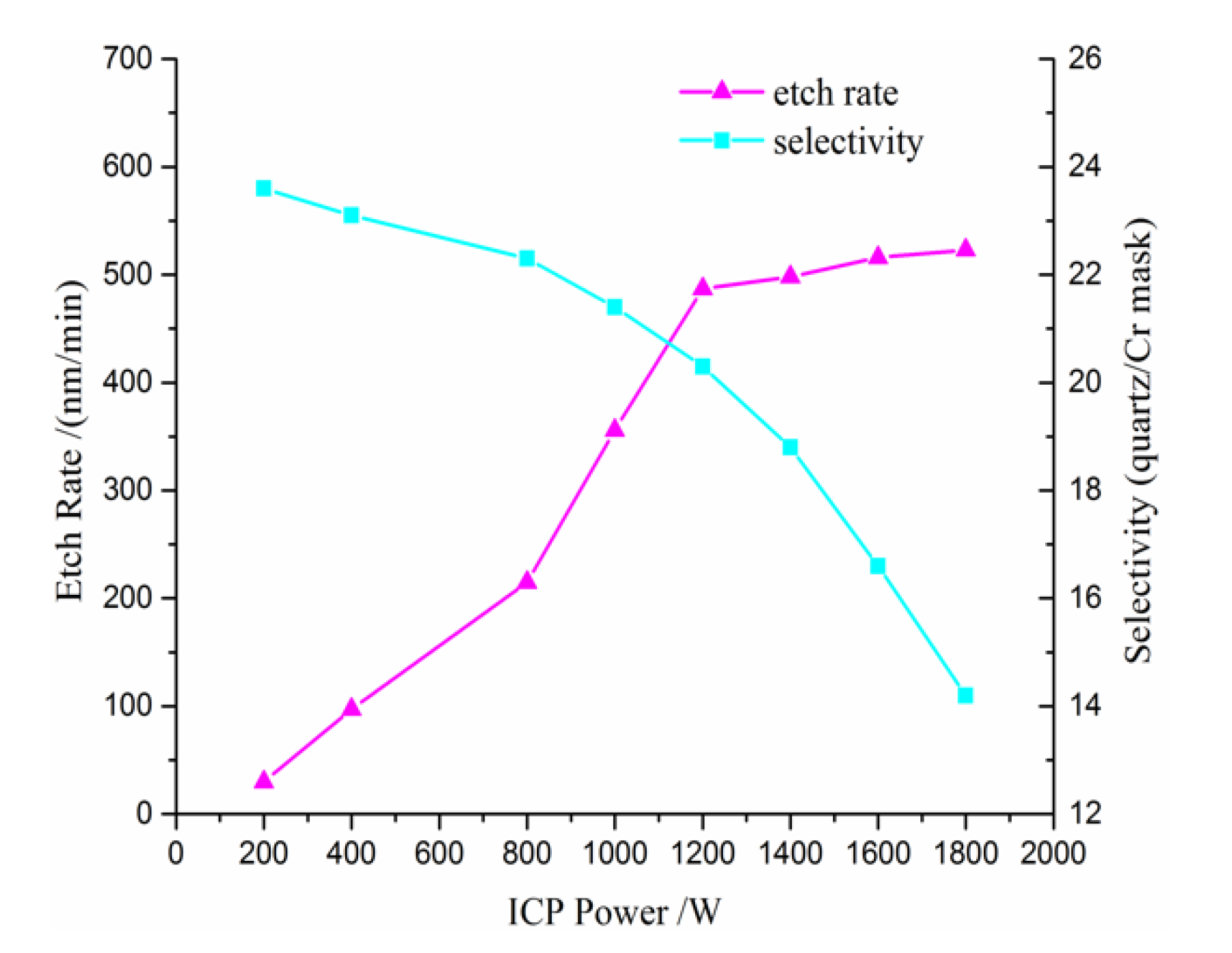
3.3. Effect of ICP Power

The ICP power has an influence on the dissociation rate of the chemical gas. In other words, a higher dissociation rate leads to a higher etching rate. In Figure 6, the etch rate of the quartz and selectivity are plotted versus the ICP power, while keeping bias power = 200 W, gas pressure = 6 mT and gas total flow rate = 110 sccm. It is seen that the etch rate increases with ICP power, due to the increase in the reactive ion flux to the substrate surface. In other words, the increasing ICP power leads to the concentration of the plasma and the dissociation rate of the chemical gas increases correspondingly. Additionally, when the ICP power increases from 1200 W to 1600 W, the increase trend of the etch rate is diminished, which is caused by the fact that the most chemical gas has been ionized when the ICP power reaches 1200 W. However, the selectivity decreases with the ICP power increase. When the ICP power increases from 1200 W to 1600 W, the decrease trend of selectivity is enhanced. Thus, it is obvious that the optimal ICP power is 1200 W.

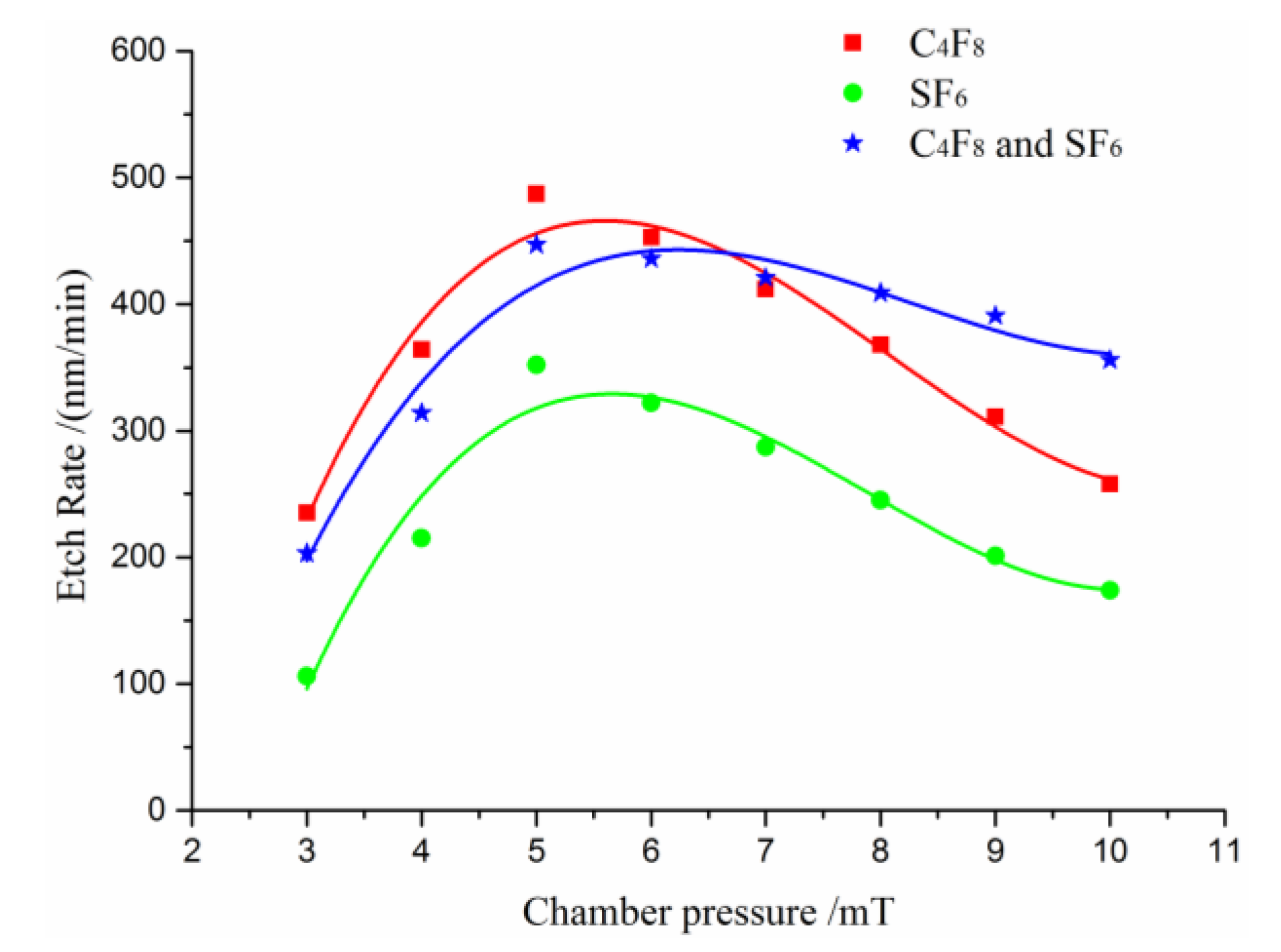
3.4. Effect of Chamber Pressure
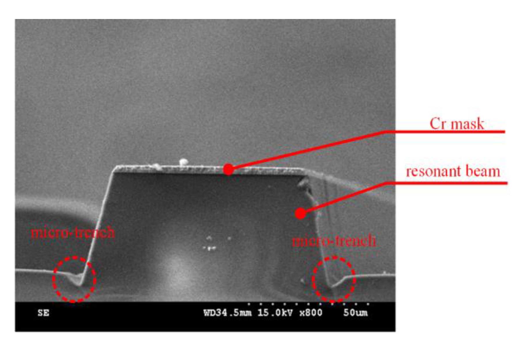
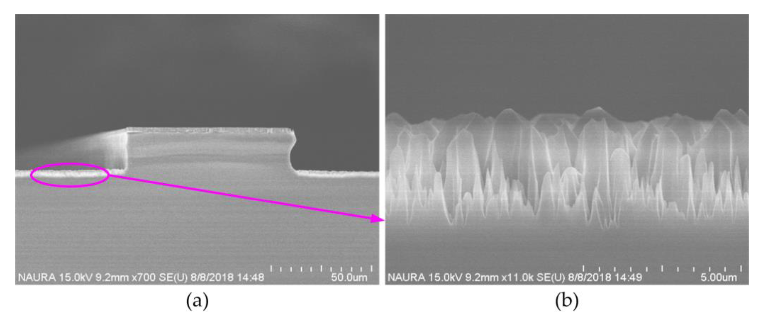
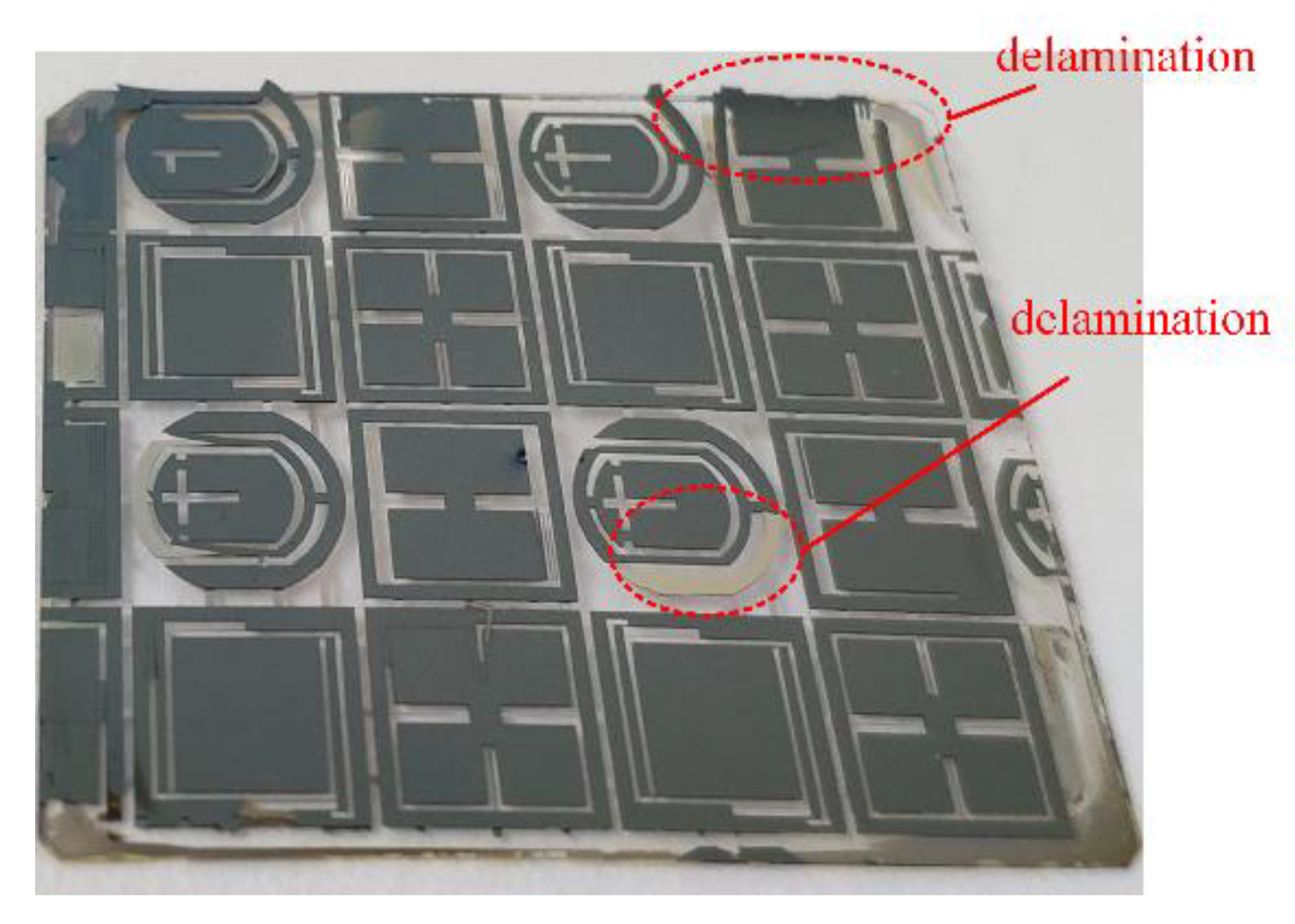
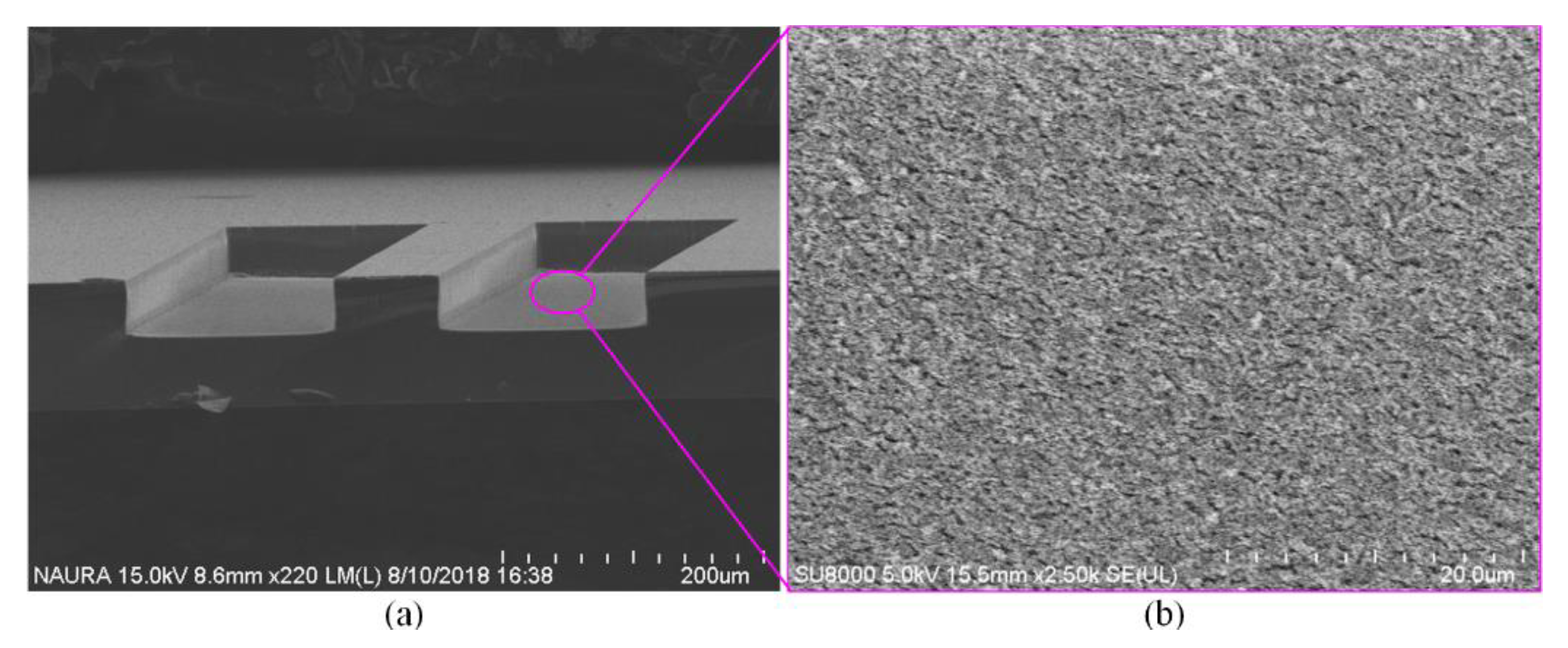
Experiments were implemented to investigate the relationship between the chamber pressure and etch rate. Figure 7 shows the etch rates of the quartz as a function of the chamber gas pressure. The pressure ranges from 3 mT to 10 mT. When the chamber pressure is lower than 5 mT, it is observed that lower pressure leads to a slower quartz etch rate. This may be due to the fact that at lower pressure the concentrations of radicals are highly reduced and the etching rate is diminished; however, when the chamber pressure is too high, the frequency of ion–ion scattering collisions is highly increased due to the reduction of the mean free path of ions, which results in a decrease in the effects of ion bombardments and a reduction in the quartz etch rate.
Compared with the single gas C4F8 and SF6, the mixture gas of C4F8 and SF6 show a better performance when the chamber pressure is greater than 5 mT. It is observed that the etch rate reduces slowly when pressure increases from 5 mT to 10 mT. It is believed that the presence of fluorine and CxFy ions in the plasma, due to high pressure, results in a reduction in concentration of the reactive etchants in this case. Therefore, the chamber gas pressure should be maintained within 4.5~6.5 mT.

3.5. Effect of Mask

Three kinds of metal masks (Ti, Al and Cr) were investigated to achieve high etch selectivity in this work—note, the ICP power, bias power, etch gas and chamber pressure are the same and shown in Table 1. The etch rate, selectivity and profile were measured for quartz with an original thickness of 300 μm. As shown in Figure 8, for the Al mask with an original thickness of about 1.8 μm, the selectivity is approximately 6 and the profile is less than 76°. For the Ti mask with an original thickness of approximately 2.4 μm, the selectivity is 10.92 and the profile is less than 84°, as shown in Figure 9. For the Cr mask with an original thickness of about 4.92 μm, the selectivity is 20.06 and the profile is vertical, as shown in Figure 10.
Table 1 shows the acquired highest quartz etch rates from all the design of experiment (DOE) runs performed in this test. The highest quartz etch rate was acquired using the C4F8 and SF6 gas combination. According to the research results above, the initial set of etching parameters are listed in Table 1. It can be found that the Cr mask can obtain a higher etch rate and selectivity. The sidewall profile with a Cr mask is more vertical in contrast to that with the Ti mask and Al mask. Moreover, in the sputtering process, the adhesion performance of Cr is superior to the others, which benefits the fabrication of a thicker mask. Hence, the Cr mask is a more appropriate choice for the deep quartz etch process.

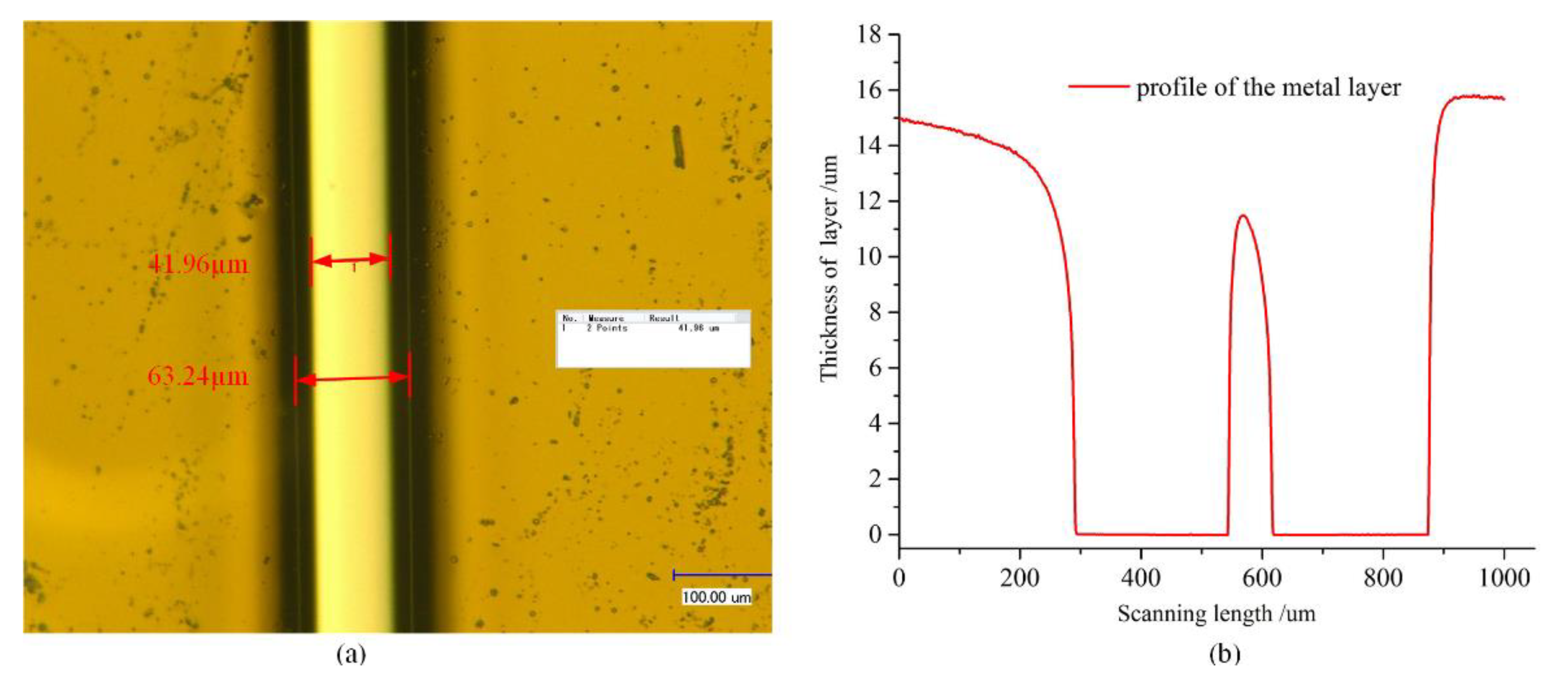
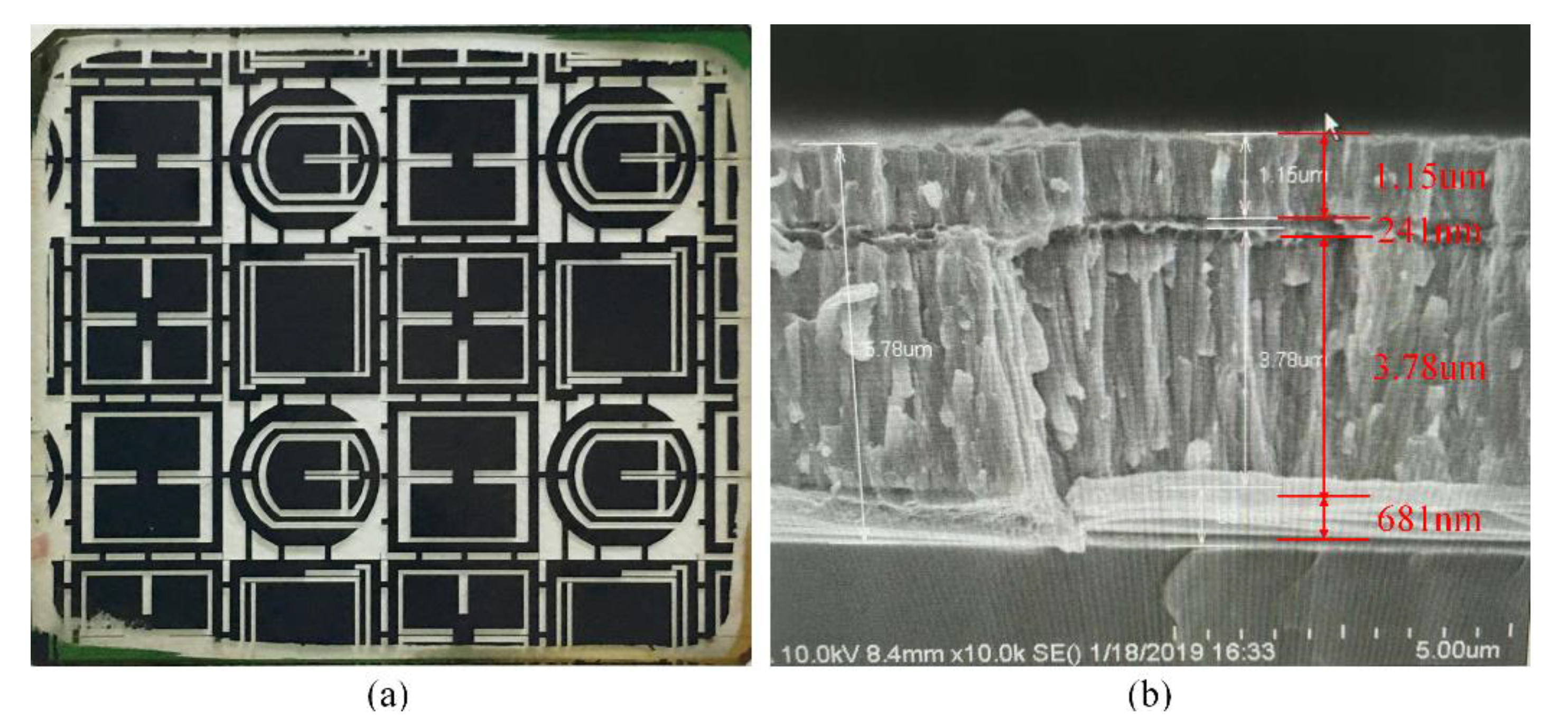
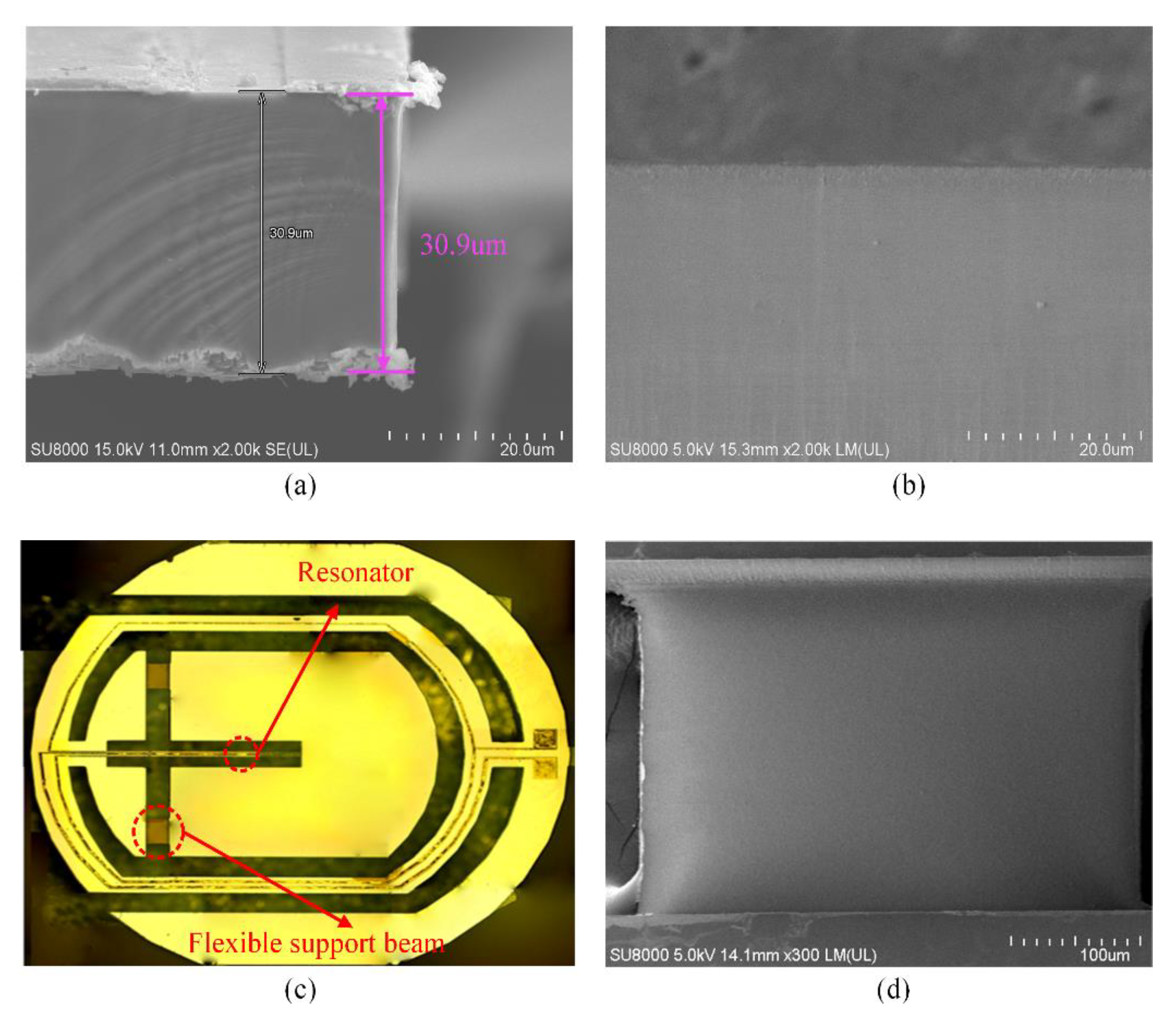
3.6. Preparation of the Thick Cr Mask

In order to achieve deep etching, a thick Cr layer should be prepared. Normally, to reduce the production time, the electrodeposited technology is applied to manufacture a thick metal layer. However, it is difficult to pattern the metal layer, and the verticality of the sidewall inclines downward with the increase in thickness, which has an undesirable effect on the sidewall and profile of the etched quartz, as shown in Figure 11. It is obvious that the metal layer fabricated by electrodeposited technology is not suitable for microstructure. Thus, the Magnetron sputtering process is selected to deposit the mask layer.
It is noticeable that the residual stress increases in the Cr layer with the thickness increase. As shown in Figure 12, the delamination issue of the Cr layer is induced by residual stress when the thickness is increased. In order to overcome the delamination issue, a “sandwich” structure composed of Al layer-Cr layer-Al layer-Cr layer is proposed, as shown in Figure 13. The Al film can play the role of releasing stress and protecting gold electrodes, which can enhance the thickness of the metal mask. In addition, the temperature of the Magnetron sputtering process is less than 50 °C. The ultrasonic cleaning machine is used for achieving a clean lift-off process, and the picture of the manufactured mask layer is shown in Figure 13a.

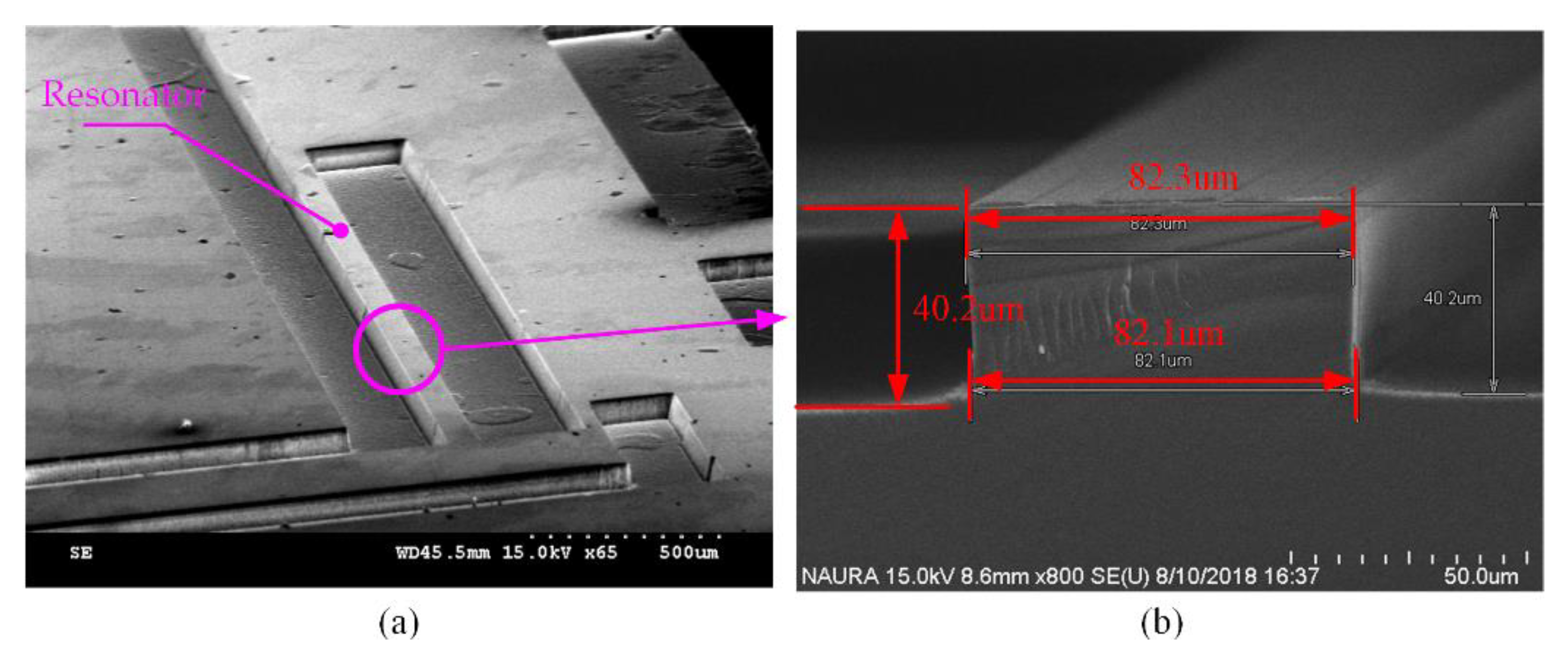
3.7. Statistic of the Experiments

In order to verify the repeatability and feasibility of the quartz etching technology, three repeated experiments were carried out and tested. In each experiment, five samples are selected and tested. The parameters of the optimized etching process are shown in Table 2. The etching time is 155 min and the desired etching depth is 70 μm. The etching depth of each sample was measured, and the statistical results of the experiments are shown in Table 3. It is clear to see that the etching rate of the quartz is about 0.45 μm/min. The statistical results demonstrate that the repeatability and consistency of the process is good.

4. Discussion

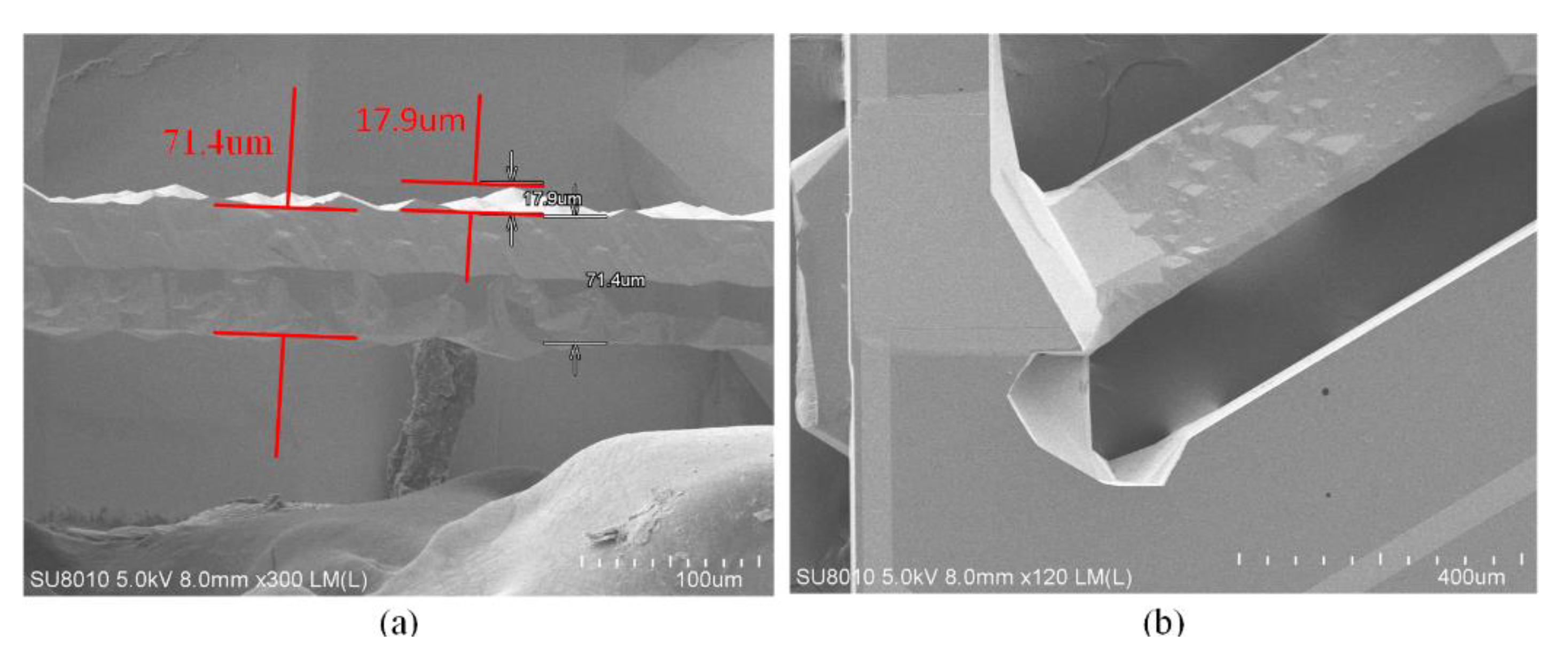
4.1. Summary of the Quartz Deep Etching Technology

The quartz deep etching process was performed with a deep reactive ion etching (DRIE) system in this paper. The optimal technological results for three kinds of etching gas are shown in Table 4. It can be observed that the gas chemistry of C4F8/SF6/Ar is the optimization. The SEM images of the etch resonator profile and cross-section view are shown in Figure 14. It can be seen that the sidewall is vertical, as shown in Figure 14b. It is feasible to manufacture quartz resonators with proposed dry deep etching process technology.
As shown in Table 1, the etch rate for C4F8/SF6/Ar is significantly lower when using an Al mask and a Ti mask than with a Cr mask. Al, while resistant to RIE thinning, is still sputtered somewhat and redeposits on the target material forming a layer which inhibits etching. This effect is alleviated for increasing Ar proportions. Cr does not noticeably reduce the etch rate because there is no shadow mask. The etching rate is very low in the low bias voltage when SF6 is the etch gas, mainly because the effective ions are lesser in contrast to C4F8. When the bias is increased, the etch rate of the C4F8 exceeds that of SF6, which states that CFx is more suitable as the plasma constituent in etching quartz than SFx. When the C4F8 proportion is increased overly, the etching rate reduces because of the forming polymer on top of quartz.
Only when the bias power is sufficient, does the etching takes place because of two reasons; (1) the steady-state polymer is thinner with higher ion energies and (2) the ion energies are high enough to break the oxide bonds. However, the roughness of the etched surface deteriorates when the bias power is excessively high. In order to reduce the surface roughness, the bias power is investigated to obtain a smooth surface. The lower bias power is beneficial and improves the smoothness and flatness of the etched surface. Moreover, during the etching process, a clean step with Ar and O2 is employed to clear away the by-product every 10 min. The parameters of clean step are shown in Table 5. The SEM images of the etched surface are shown in Figure 15. It is obvious that the clean step is conductive to the improvement of the etched surface.
In this work, the focus of our attention is the smoothness of the etched surface and verticality of the sidewall. Moreover, an appropriate etching rate should be obtained to realize a deep etching depth. Table 6 shows the characteristics of the proposed etch technology compared with the previously published literatures. Compared with other research, the results proposed in this work can obtain a higher performance, such as profile and etch rate, although the selectivity is less than that proposed by V. Bliznetsov [22]. However, the mask material presented by V. Bliznetsov was AlN, which is defective as the AlN is unaccommodated to the fabrication of a thick mask. In the sputtering and evaporation process, the deposition rate of AlN is much less than that of Cr (the deposition rate of AlN is about 3 nm/min; the deposition rate of Cr is about 20 nm/min). From the research carried out by K. Kolari [42], it can be seen that the selectivity with a Ni mask is near to a Cr mask; in the research carried out by M. Esashi [9], a higher selectivity was achieved, possibly because the etching depth is shallower than that in this work. Nevertheless, the verticality of the sidewall presented by M. Esashi and K. Kolari is less than that presented in this paper, which has a significant effect on the performance of quartz resonators. Thus, the etch technology presented in this paper is more suitable for dry deep quartz etching.
It is worthwhile to mention that the substrate temperature is also a significant factor for reducing the roughness of the sidewall and etching bottom, since a thick polymer layer deposited on the sidewalls and bottom could induce a micro-masking effect, which is a possible factor causing the etched sidewall and bottom roughness. As measured by using the ellipsometer, there were no detectable polymer layers deposited on the samples during the etching. The reason for this was that the substrate temperature was relatively high (90 °C) in our case, so that the deposited polymer layer may been too thin to be detected. This could be of benefit to the reduction in the sidewall and bottom roughness of the etched trench. The pictures of the etched quartz structure with a scanning electron microscope (SEM) and a light microscope are shown in Figure 16. They indicate that the proposed deep quartz etch process technology is credible and feasible.

4.2. Compared with Other Quartz Etching Technology

The structure of the etched quartz with wet chemical etching technology is shown in Figure 17. There are some pyramid structures on the etched sidewall and bottom, which have an adverse effect on the performance of quartz resonators such as stability, reliability and accuracy. It is clear to see that the smoothness of the sidewall and bottom is poor; hence the performance of wet chemical etching technology needs to be improved to meet the requirements of quartz resonators fabrication. The structure of the etched quartz with the proposed deep quartz etch process technology is shown in Figure 18. It is obvious to see that the profile of the etched sidewall and bottom is smooth, which is very necessary and significant to manufacture a quartz resonator.
The ECDM and laser ablation techniques are also used for glass-based material etching in some structures such as micro-channels and holes. The etching rate of them is faster than that of the plasma-based etching technique. However, the ECDM and laser ablation techniques are not suitable for alpha quartz crystal resonant device fabrication. In general, the resonant device structures are much more complex than the micro-channels and holes, and thus the fabrication efficiencies of ECDM techniques and laser ablation are too low to manufacture complex structures and mass production. Moreover, the laser energy results in a quartz crystal denaturation at the edge of the resonant beam in laser ablation technology, as shown in Figure 19a; the roughness and flatness of the etched bottom and sidewall cannot meet the accuracy requirements of the resonator in laser ablation and ECDM technology, which induces an adverse effect on the performance of the quartz resonators. Therefore, the plasma etching technology should be a better choice for quartz resonant device fabrication and the etched quartz resonator is shown in Figure 19b. It is obvious to see that the quartz resonator etched by the proposed etching technology is feasible.
The pictures of the etched MEMS resonant device and the smoothness of the etched surface are shown in Figure 20. The thickness of the quartz resonator is about 30.9 µm, which is very close to the desired thickness (30 µm). The etched sidewall of the resonator is shown in Figure 20b; it is obvious to see that the etched sidewall is smooth and complanate. The etched bottom of the flexible support beam is shown in Figure 20d, which is smooth and complanate. Therefore, the proposed quartz etching technology can obtain a smooth and complanate etched surface, and the accuracy of the etching technology can meet the requirements of MEMS quartz resonant devices.

5. Conclusions

In this paper, we investigated the optimization of deep etching with hard masks for quartz crystal. Comparing C4F8/Ar, SF6/Ar and C4F8/SF6/Ar, the third one provided the fewest by-products re-deposited on the sidewalls and bottom, enabled an etching sidewall closer to vertical and an acceptable etching rate. Hence, it is the most suitable for deep quartz etching and high aspect ratio etching. Research on bias power and ICP power were carried out to optimize the etching process parameters. Out of the three studied metal masks, Al, Ti and Cr, the last mask yields the highest selectivity and etching rate. Moreover, the profile of the sidewall with a Cr mask is nearly vertical due to the reduction in by-products re-deposited on the sidewalls and bottom. An optimized etching process with C4F8/SF6/Ar generated an etched trench with a depth of 75.4 µm. The smoothness of the etched surface and verticality of the sidewall meet the requirements of MEMS resonant device fabrication. Based on the confirmed selectivity and Cr mask, it can be expected that the etching capability presented in this work is extendable to the etching of quartz to a depth of around 100 µm.

Author Contributions

Data curation, C.H. and Q.Z.; Investigation, B.L.; Methodology, C.L.; Project administration, Y.Z. All authors have read and agreed to the published version of the manuscript.

Funding

This work was supported in part by the National Key R&D Program of China (2017YFB1102900), the National Natural Science Foundation of China (Grant No. 51805424) and the Key R&D Program of Shaanxi Province (Grant No. 2018ZDCXL-GY-02-03).

Conflicts of Interest

The authors declare no conflict of interest.

References

  1. Hung, C.-H.; Wang, W.-S.; Lin, Y.-C.; Liu, T.-W.; Sun, J.-H.; Chen, Y.-Y.; Esashi, M.; Wu, T.-T. Design and fabrication of an AT-cut quartz phononic Lamb wave resonator. J. Micromech. Microeng. 2013, 23, 065025. [Google Scholar] [CrossRef]
  2. Hussain, D.; Wen, Y.; Hui, X. Sidewall Imaging of Microstructures with a Tilted Quartz Tuning Fork (QTF) Force Sensor. In Proceedings of the 2018 International Conference on Manipulation, Automation and Robotics at Small Scales (MARSS), Nagoya, Japan, 4–8 July 2018. [Google Scholar]
  3. Li, B.; Zhao, Y.; Li, C.; Cheng, R.; Sun, D.; Wang, S. A Differential Resonant Accelerometer with Low Cross-Interference and Temperature Drift. Sensors 2017, 17, 178. [Google Scholar] [CrossRef] [Green Version]
  4. Abe, T.; Esashi, M. One-chip multichannel quartz crystal microbalance (QCM) fabricated by Deep RIE. Sensors Actuators A-Phys. 2000, 82, 139–143. [Google Scholar] [CrossRef]
  5. Abe, T.; Itasaka, Y. A fabrication method of high-Q quartz crystal resonator using double-layered etching mask for DRIE. Sensors Actuators A-Phys. 2012, 188, 503–506. [Google Scholar] [CrossRef]
  6. Girault, P.; Lorrain, N.; Lemaitre, J.; Poffo, L.; Guendouz, M.; Hardy, I.; Gadonna, M.; Gutierrez, A.; Bodiou, L.; Charrier, J. Racetrack micro-resonators based on ridge waveguides made of porous silica. Opt. Mater. 2015, 50, 167–174. [Google Scholar] [CrossRef] [Green Version]
  7. Nanto, H.; Yokoi, Y.; Mukai, T.; Fujioka, J.; Kusano, E.; Kinbara, A.; Douguchi, Y. Novel gas sensor using polymer-film-coated quartz resonator for environmental monitoring. Mater. Sci. Eng. C-Biomim. Supramol. Syst. 2000, 12, 43–48. [Google Scholar] [CrossRef]
  8. Papp, S.B.; Diddams, S.A. Spectral and temporal characterization of a fused-quartz microresonator optical frequency comb. Phys. Rev. A 2011, 84, 6302–6312. [Google Scholar] [CrossRef] [Green Version]
  9. Song, E.-S.; Kang, S.; Kim, H.; Kim, Y.-K.; An, J.-E.; Baek, C.-W. Wafer-Level Fabrication of a Fused-Quartz Double-Ended Tuning Fork Resonator Oscillator Using Quartz-on-Quartz Direct Bonding. IEEE Electron Device Lett. 2013, 34, 692–694. [Google Scholar] [CrossRef]
  10. Zhou, L.; Zhong, Q.; Li, J.; Xing, H.; Wang, X.; Zhou, Z.; Wang, X. Design and Fabrication of a Novel 5 times 5 Beam Dammann Grating. Micronanoelectron. Technol. 2018, 55, 677–682. [Google Scholar]
  11. Lazorina, E.I.; Soroka, V.V. Etching of quartz and some features of the surface layer. Sov. Phys. Crystallogr. 1974, 18, 651–653. [Google Scholar]
  12. Tellier, C.R. some results on chemical etching of at-cut quartz wafers in ammonium bifluoride solutions. J. Mater. Sci. 1982, 17, 1348–1354. [Google Scholar] [CrossRef]
  13. Xing, Y.; Gosalvez, M.A.; Zhang, H.; Li, Y.; Qiu, X. Transient and Stable Profiles during Anisotropic Wet Etching of Quartz. J. Microelectromechanical Syst. 2017, 26, 1063–1072. [Google Scholar] [CrossRef]
  14. Varel, H.; Ashkenasi, D.; Rosenfeld, A.; Wahmer, M.; Campbell, E.E.B. Micromachining of quartz with ultrashort laser pulses. Appl. Phys. A-Mater. Sci. Process. 1997, 65, 367–373. [Google Scholar] [CrossRef]
  15. Moridi, A.; Wang, J.; Ali, Y.M.; Mathew, P.; Li, X. A Study of Abrasive Jet Micro-Grooving of Quartz Crystals. In Advances in Materials Processing Ix; Wang, J., Mathew, P., Li, X.P., Huang, C.Z., Zhu, H.T., Eds.; Trans Tech Publications Ltd.: Stafa-Zurich, Switzerland, 2010; p. 645. [Google Scholar]
  16. Wang, J.; Moridi, A.; Mathew, P. Micro-grooving on quartz crystals by an abrasive air jet. Proc. Inst. Mech. Eng. Part C J. Mech. Eng. Sci. 2011, 225, 2161–2173. [Google Scholar] [CrossRef]
  17. Chen, X.; Tian, C.; Huang, Y.; Li, D.; Wang, H.; Zhang, W. Surface quality for rotary ultrasonic milling of quartz glass employing diamond ball end tool with tool inclination angle. In Proceedings of the 13th Global Congress on Manufacturing and Management, Zhengzhou, China, 28–30 November 2016; pp. 360–369. [Google Scholar]
  18. Kamaraj, A.B.; Jui, S.K.; Cai, Z.; Sundaram, M.M. A mathematical model to predict overcut during electrochemical discharge machining. Int. J. Adv. Manuf. Technol. 2015, 81, 685–691. [Google Scholar] [CrossRef]
  19. Khac-Ha, N.; Lee, P.A.; Kim, B.H. Experimental Investigation of ECDM for Fabricating Micro Structures of Quartz. Int. J. Precis. Eng. Manuf. 2015, 16, 5–12. [Google Scholar]
  20. Saranya, S.; Sankar, A.R. Fabrication of precise micro-holes on quartz substrates with improved aspect ratio using a constant velocity-feed drilling technique of an ECDM process. J. Micromech. Microeng. 2018, 28, 125009. [Google Scholar] [CrossRef]
  21. Saranya, S.; Sankar, A.R.; IEEE. Effect of Tool Shape and Tool Feed Rate on the Machined Profile of a Quartz Substrate Using an Electrochemical Discharge Machining Process. In Proceedings of the 2015 2nd International Symposium on Physics and Technology of Sensors (ISPTS), Pune, India, 7–10 March 2015. [Google Scholar]
  22. Bliznetsov, V.; Lin, H.M.; Zhang, Y.J.; Johnson, D. Deep SiO2 etching with Al and AlN masks for MEMS devices. J. Micromech. Microeng. 2015, 25, 87002. [Google Scholar] [CrossRef] [Green Version]
  23. Chapellier, P.; Verlhac, B.; Lavenus, P.; Dulmet, B.; IEEE. DRIE of high Q-factor length-extensional mode quartz micro-resonator. In Proceedings of the 2017 Joint Conference of the European Frequency and Time Forum and Ieee International Frequency Control Symposium, Besançon, France, 9–13 July 2017; pp. 218–221. [Google Scholar]
  24. Ichiki, T.; Sugiyama, Y.; Ujiie, T.; Horiike, Y. Deep dry etching of borosilicate glass using fluorine-based high-density plasmas for micrbelectromechanical system fabrication. J. Vac. Sci. Technol. B 2003, 21, 2188–2192. [Google Scholar] [CrossRef]
  25. Kamijo, A.; Monoe, S.; Murayama, N.; Saito, T.; Kimura, N.; IEEE. Wafer-Level Quartz Dry Etching Technolog. In Proceedings of the 2014 IEEE International Frequency Control Symposium, Taipei, Taiwan, 19–22 May 2014; pp. 80–83. [Google Scholar]
  26. Kim, J.S.; Jeong, H.W.; Lee, W.; Park, B.G.; Kim, B.M.; Lee, K.B. A simple and fast fabrication of a both self-cleanable and deep-UV antireflective quartz nanostructured surface. Nanoscale Res. Lett. 2012, 7, 430. [Google Scholar] [CrossRef] [Green Version]
  27. Kimura, S.; Imai, Y. Parabolic refractive X-ray lenses made of quartz glass for high-energy X-ray focusing. Jpn. J. Appl. Phys. 2016, 55, 38001. [Google Scholar] [CrossRef]
  28. Kolari, K. High etch selectivity for plasma etching SiO2 with AlN and Al2O3 masks. Microelectron. Eng. 2008, 85, 985–987. [Google Scholar] [CrossRef]
  29. Li, W.T.; Bulla, D.A.P.; Love, J.; Luther-Davies, B.; Charles, C.; Boswell, R. Deep dry-etch of silica in a helicon plasma etcher for optical waveguide fabricatlon. J. Vac. Sci. Technol. A 2005, 23, 146–150. [Google Scholar] [CrossRef]
  30. Minnick, M.D.; Devenyi, G.A.; Kleiman, R.N. Optimum reactive ion etching of x-cut quartz using SF6 and Ar. J. Micromech. Microeng. 2013, 23, 117002. [Google Scholar] [CrossRef]
  31. Odinokov, S.B.; Sagatelyan, G.R.; Kovalev, M.S.; Bugorkov, K.N. Features of the plasma-chemical etching of quartz glass during the formation of deep surface relief on high-precision components of devices. J. Opt. Technol. 2019, 86, 317–322. [Google Scholar] [CrossRef]
  32. Osipov, A.A.; Aleksandrov, S.E.; Osipov, A.A.; Berezenko, V.I. Development of Process for Fast Plasma-Chemical Through Etching of Single-Crystal Quartz in SF6/O-2 Gas Mixture. Russ. J. Appl. Chem. 2018, 91, 1255–1261. [Google Scholar] [CrossRef]
  33. Pedersen, M.; Huff, M. Plasma Etching of Deep High-Aspect Ratio Features Into Fused Silica. J. Microelectronmech. Syst. 2017, 26, 448–455. [Google Scholar] [CrossRef]
  34. Perros, A.; Bosund, M.; Sajavaara, T.; Laitinen, M.; Sainiemi, L.; Huhtio, T.; Lipsanen, H. Plasma etch characteristics of aluminum nitride mask layers grown by low-temperature plasma enhanced atomic layer deposition in SF6 based plasmas. J. Vac. Science Technol. A 2012, 30, 11504. [Google Scholar] [CrossRef] [Green Version]
  35. Tang, Y.-H.; Lin, Y.-H.; Chen, P.-L.; Shiao, M.-H.; Hsiao, C.-N. Comparison of optimised conditions for inductively coupled plasma-reactive ion etching of quartz substrates and its optical applications. Micro Nano Lett. 2014, 9, 395–398. [Google Scholar] [CrossRef]
  36. Tang, Y.-H.; Lin, Y.-H.; Huang, T.-T.; Wang, J.-S.; Shiao, M.-H.; Yu, C.-S.; IEEE. Investigation of Fabricated Through Glass Via (TGV) Process by Inductively Coupled Plasma Reactive Ion Etching of Quartz Glass. In Proceedings of the 2015 IEEE 10th International Conference on Nano/Micro Engineered and Molecular Systems, Xi’an, China, 7–11 April 2015; pp. 401–404. [Google Scholar]
  37. Chen, H.; Fu, C. An investigation into the characteristics of deep reactive ion etching of quartz using SU-8 as a mask. J. Micromech. Microeng. 2008, 18, 105001. [Google Scholar] [CrossRef]
  38. Kolari, K.; Saarela, V.; Franssila, S. Deep plasma etching of glass for fluidic devices with different mask materials. J. Micromech. Microeng. 2008, 18, 064010. [Google Scholar] [CrossRef]
  39. Li, L.; Abe, T.; Esashi, M. Smooth surface glass etching by deep reactive ion etching with SF6 and Xe gases. J. Vac. Sci. Technol. B 2003, 21, 2545–2549. [Google Scholar] [CrossRef]
  40. Mohamed, K.; Alkaisi, M.M. Investigation of a nanofabrication process to achieve high aspect-ratio nanostructures on a quartz substrate. Nanotechnology 2013, 24, 015302. [Google Scholar] [CrossRef]
  41. Ray, T.; Zhu, H.; Meldrum, D.R. Deep reactive ion etching of fused silica using a single-coated soft mask layer for bio-analytical applications. J. Micromech. Microeng. 2010, 20, 97002. [Google Scholar] [CrossRef]
  42. Tang, Y.-H.; Huang, M.-J.; Su, J.-Y.; Shiao, M.-H. Fabrication of Nanocone Subwavelength Antireflection Structures on Quartz Substrates. Jpn. J. Appl. Phys. 2012, 51, 06FF06. [Google Scholar] [CrossRef]
  43. Zeze, D.A.; Forrest, R.D.; Carey, J.D.; Cox, D.C.; Robertson, I.D.; Weiss, B.L.; Silva, S.R.P. Reactive ion etching of quartz and Pyrex for microelectronic applications. J. Appl. Phys. 2002, 92, 3624–3629. [Google Scholar] [CrossRef] [Green Version]
  44. Li, W.-T.; Bulla, D.A.P.; Boswell, R. Surface oxidation of Al masks for deep dry-etch of silica optical waveguides. Surface Coat. Technol. 2007, 201, 4979–4983. [Google Scholar] [CrossRef]
  45. Hedlund, C.; Lindberg, U.; Bucht, U.; Soderkvist, J. Anisotropic etching of Z-cut quartz. J. Micromech. Microeng. 1993, 3, 65–73. [Google Scholar] [CrossRef]
  46. Zhang, H.; Xing, Y.; Li, Y.; Gosalvez, M.A.; Qiu, X. Kinetic Monte Carlo method for the simulation of anisotropic wet etching of quartz. Sensors Actuators A-Phys. 2017, 256, 24–34. [Google Scholar] [CrossRef]
  47. Zhang, H.; Xing, Y.; Zhang, J.; Gosalvez, M.A.; Li, Y.; Zhang, Y.; IEEE. Evolutionary Kinetic Monte Carlo Method for The Simulation of Anisotropic Etching of Z-Cut, At-Cut And Bt-Cut Quartz. In Proceedings of the 2017 19th International Conference on Solid-State Sensors, Actuators and Microsystems (TRANSDUCERS), Kaohsiung, Taiwan, 18–22 June 2017. [Google Scholar]
Figure 1. (a) The test results of the etching rate and sidewall angle versus the C4F8 percentage; (b) the test results of the etching rate and sidewall angle versus SF6 percentage.
Micromachines 11 00724 g001
Figure 2. (a) The test results of the etching rate and sidewall angle versus the Ar percentage; (b) the test results of the etching rate and sidewall angle versus the ratio of C4F8 and SF6.
Micromachines 11 00724 g002
Figure 3. The test results of the etching rate and selectivity influenced by bias power.
Micromachines 11 00724 g003
Figure 4. A micro-trench at the position between the sidewall and the bottom surface.
Micromachines 11 00724 g004
Figure 5. (a) Scanning Electron Microscope (SEM) picture of the rough etching bottom; (b) SEM picture of the enlarged partial bottom.
Micromachines 11 00724 g005
Figure 6. The etch rate of the quartz and selectivity versus the inductively coupled plasma (ICP) power.
Micromachines 11 00724 g006
Figure 7. The relationship between the chamber pressure and etch rate.
Micromachines 11 00724 g007
Figure 8. (a) SEM image of Al mask before the etching; (b) SEM image of the etch profile with Al mask.
Micromachines 11 00724 g008
Figure 9. (a) SEM image of Ti mask before the etching; (b) SEM image of Ti mask after the etching; (c) SEM image of the etch profile with Ti mask.
Micromachines 11 00724 g009
Figure 10. (a) SEM image of Cr mask before the etching; (b) SEM image of Cr mask after the etching; (c) SEM image of the etch profile with Cr mask.
Micromachines 11 00724 g010
Figure 11. (a) The picture of Cr layer under a light microscope; (b) the profile of Cr layer with the step profiler.
Micromachines 11 00724 g011
Figure 12. The delamination issue of the Cr layer induced by residual stress.
Micromachines 11 00724 g012
Figure 13. (a) The picture of the manufactured mask layer; (b) the SEM image of the “sandwich” structure.
Micromachines 11 00724 g013
Figure 14. (a) SEM image of etched quartz resonator; (b) the cross-section view of resonator.
Micromachines 11 00724 g014
Figure 15. (a) The SEM image of the etched surface without clean step; (b) the SEM image of the etched surface with clean step.
Micromachines 11 00724 g015
Figure 16. (a) SEM picture of the etched quartz structure; (b) the picture of the etched quartz structure under a light microscope.
Micromachines 11 00724 g016
Figure 17. (a) The profile of the etched sidewall and bottom with wet chemical etching technology; (b) the smoothness of etched bottom wet chemical etching technology.
Micromachines 11 00724 g017
Figure 18. (a) The profile of etched sidewall and bottom; (b) the roughness of etched bottom.
Micromachines 11 00724 g018
Figure 19. (a) The picture of the etched quartz structure with laser ablation under a light microscope; (b) the picture of the etched quartz structure with plasma etching under a light microscope.
Micromachines 11 00724 g019
Figure 20. (a) The cross-section SEM image of the etched quartz resonator; (b) the SEM image of the etched sidewall; (c) the picture of the etched MEMS resonant device; (d) the SEM image of the etched bottom.
Micromachines 11 00724 g020
Table 1. Etch process for each metal mask.
ParameterAl MaskTi MaskCr Mask
ICP power (W)120012001200
Bias power (W)200200200
Chamber pressure (mT)555
C4F8 (sccm)303030
SF6 (sccm)303030
Ar (sccm)606060
Etch rate of quartz (nm min−1)0.20.230.42
Selectivity (quartz/mask)610.9221.06
Profile (°)768489
Table 2. The parameters of optimized etching process.
ParametersICP Power (W)Bias Power (W)Chamber Pressure (mT)Temperature
(°C)
Ar (sccm)C4F8 (sccm)SF6 (sccm)Etching Time (min)
Value1200230690603030155
Table 3. Statistical results of three repeated experiments.
ExperimentRun 1Run 2Run 3
Sample
170.1 μm69.7 μm70.1 μm
270.4 μm69.3 μm70.2 μm
370.3 μm69.1 μm69.8 μm
469.9 μm70 μm69.6 μm
570.5 μm69.5 μm70 μm
Average value74.24 μm69.52 μm69.94 μm
Standard deviation0.240830.349280.24083
Etching rate (μm/min)0.4530.4490.451
Table 4. The results of quartz etching with three chemical gases.
Etch GasEtch Rate of Quartz
(μm/min)
Profile (°)
C4F8/Ar0.4882
SF6/Ar0.3186
C4F8/SF6/Ar0.4390
Table 5. The parameters of clean step.
ParametersICP Power (W)Bias Power (W)Chamber Pressure (mT)Temperature (°C)Ar (sccm)O2 (sccm)
Value12002005904015
Table 6. The characteristics of the proposed etch technology compared with the previously published literatures.
ParametersTargetMaskEtch Rate
(μm/min)
SelectivityProfile (Degree)Depth (μm)
H. Chen [37]quartzSU-80.220.348655
V. Bliznetsov [22]USGAlN0.32498821
Tathagata Ray [41]Fused silicaKMPR®10250.09331.138530
M. Esashi [4]quartzNi0.5308720
K. Kolari [38]PyrexTMNi0.723.378100
This workquartzCr0.4521.069075.4

