
Impact of III-Nitride/Si Interface Preconditioning on Breakdown Voltage in GaN-on-Silicon HEMT


Abstract
:1. Introduction
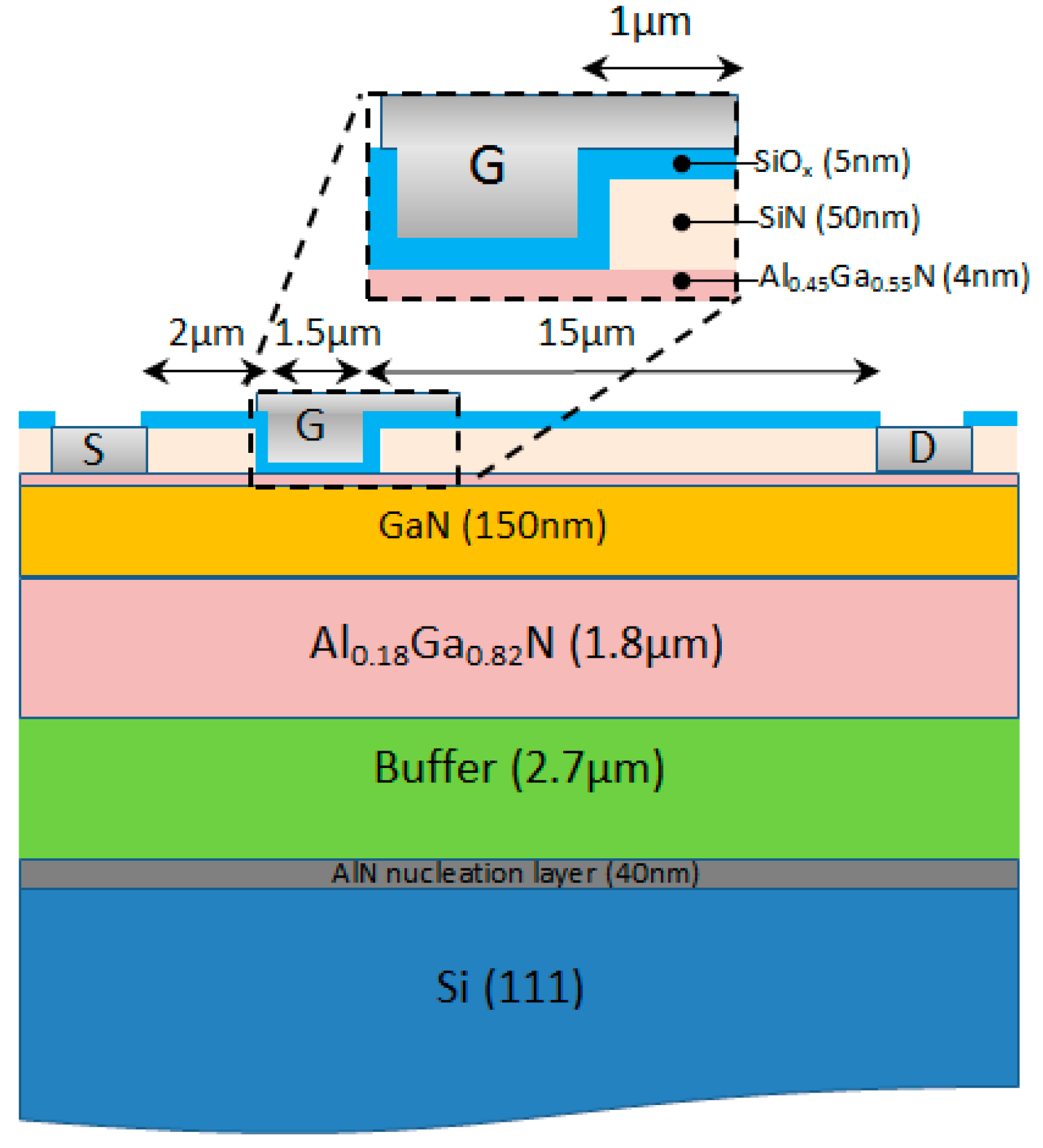
2. Materials and Methods
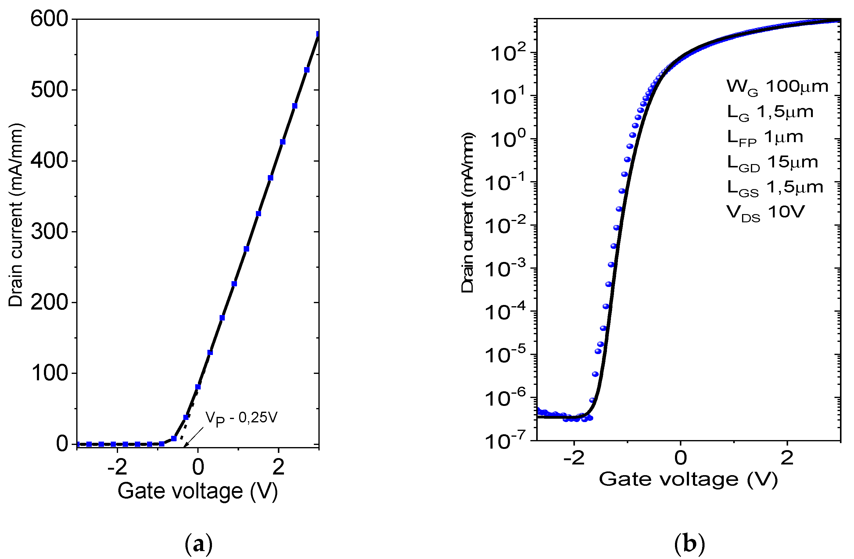
2.1. Current-Voltage Characteristics
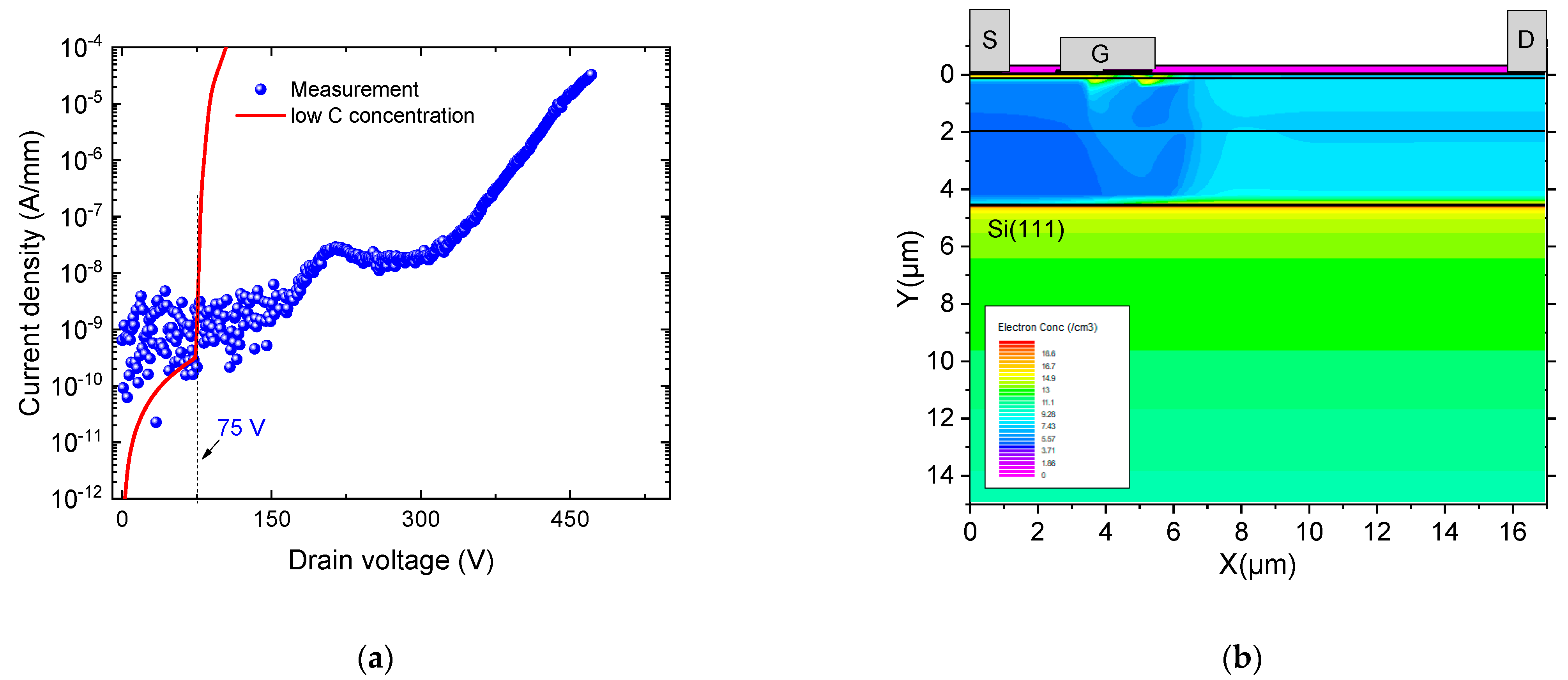
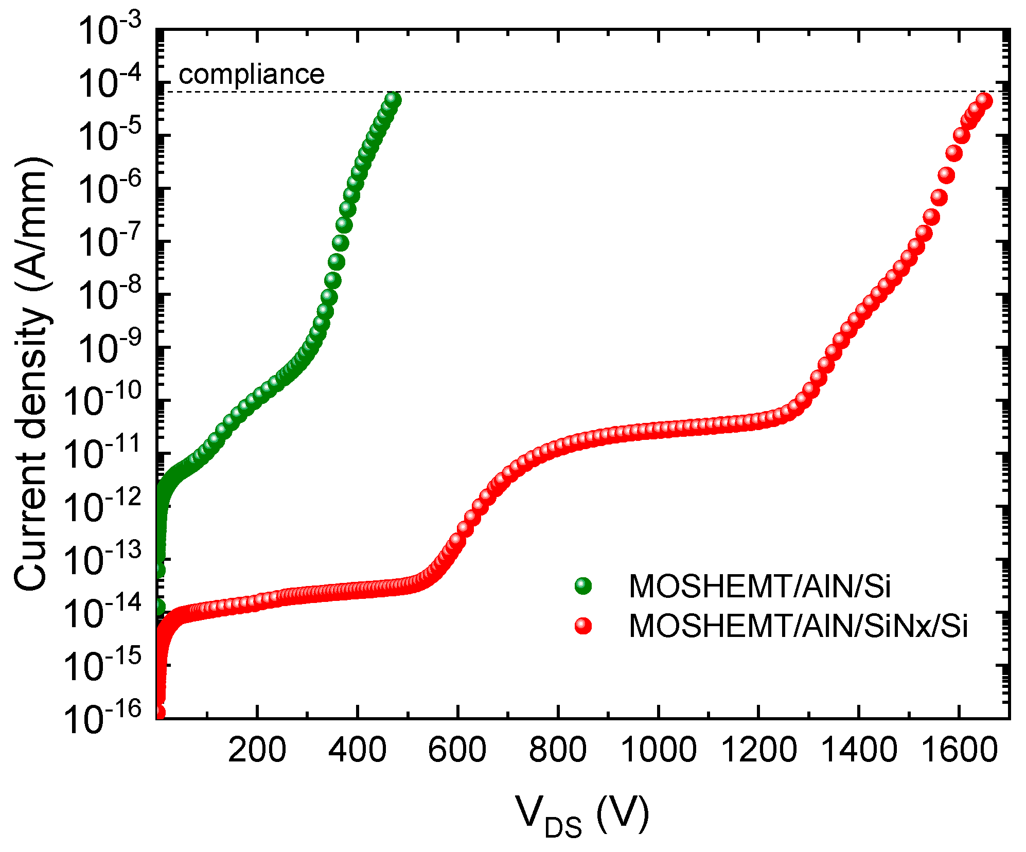
2.2. Breakdown Characteristics
3. Results
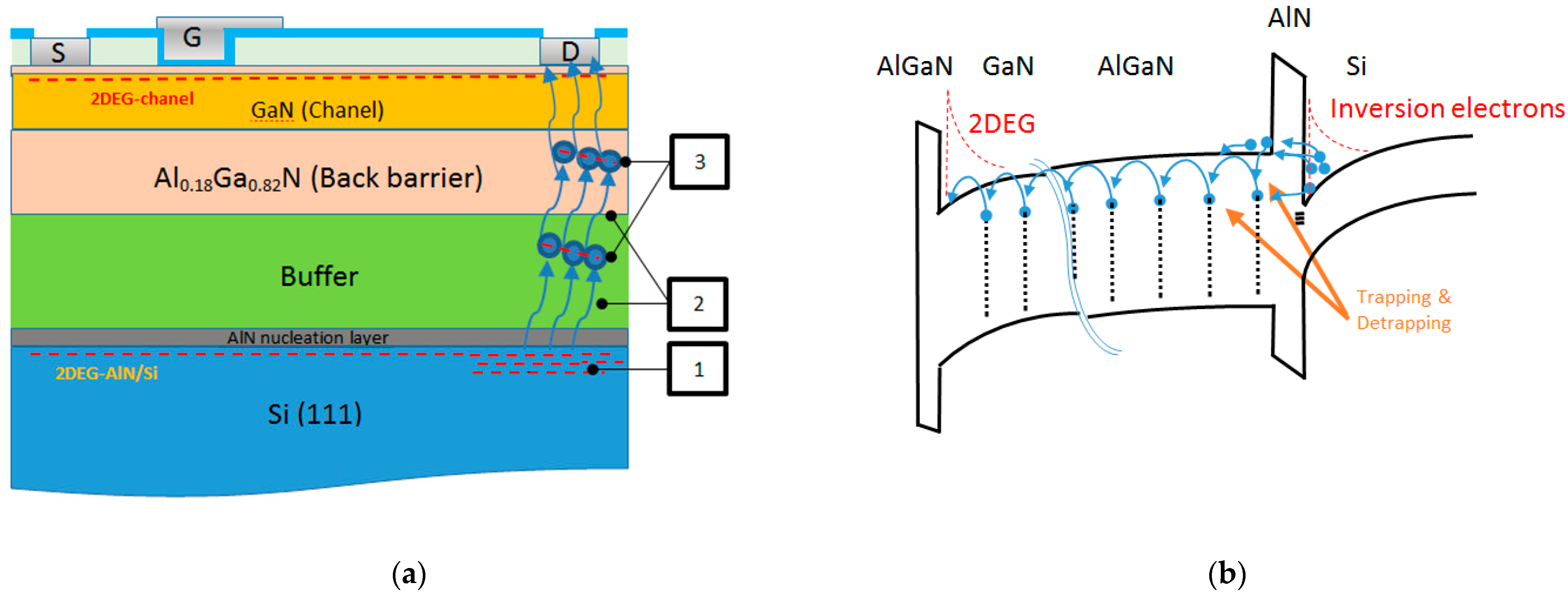
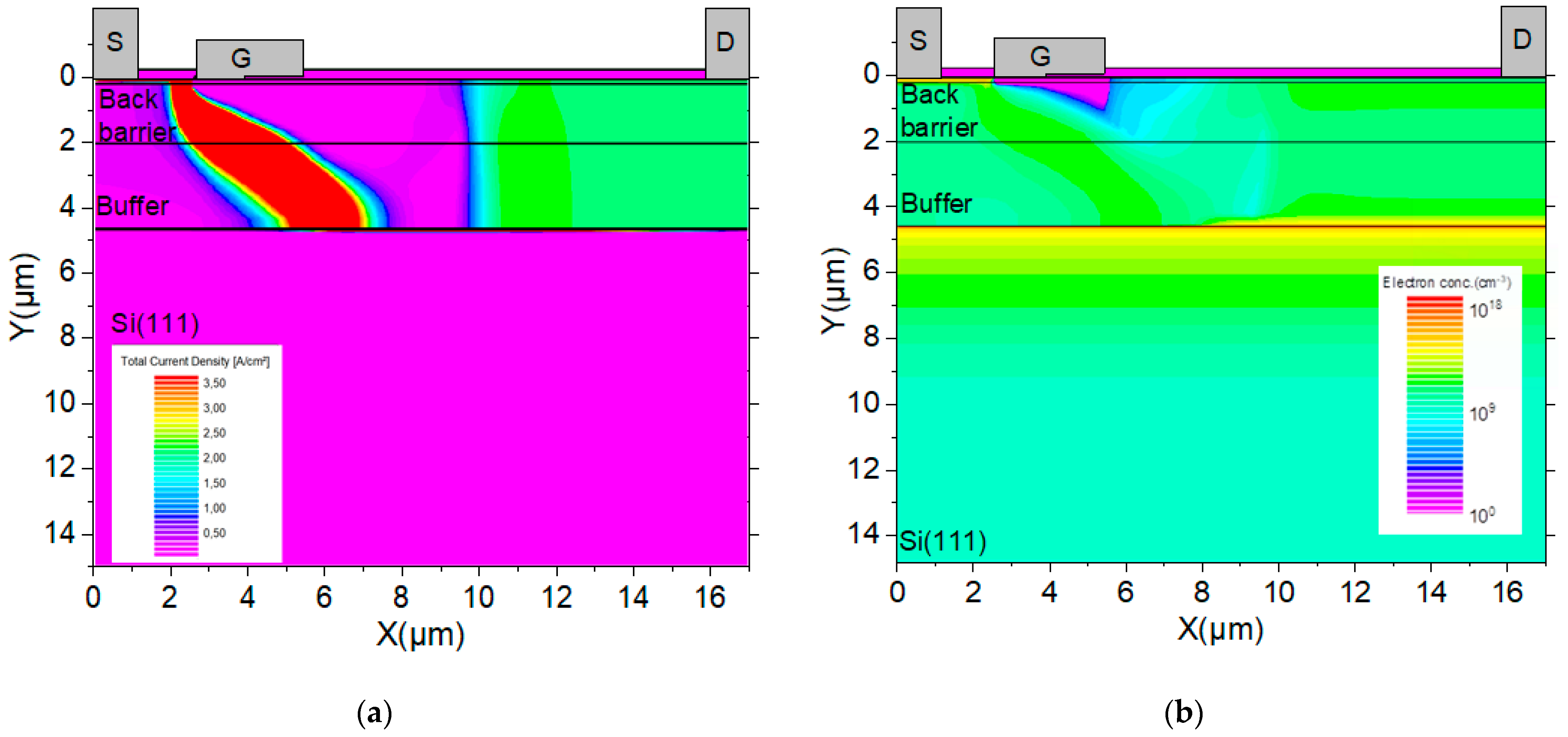
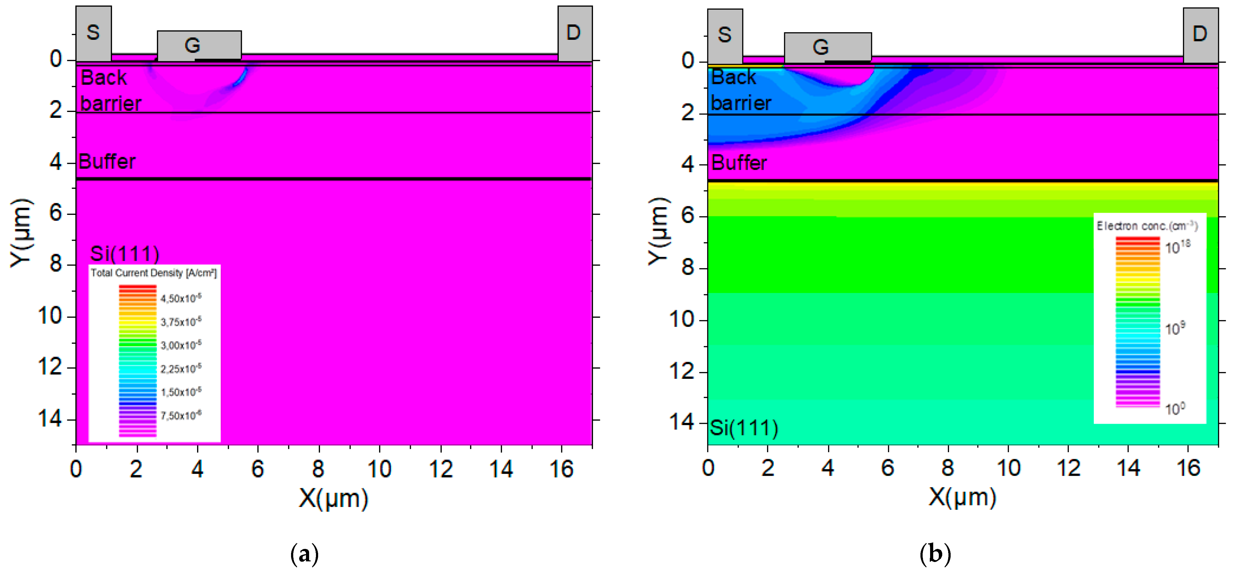
4. Discussion
4.1. Breakdown Origin
4.2. Breakdown Improvement
5. Conclusions
Author Contributions
Funding
Acknowledgments
Conflicts of Interest
References
- Rongming, C. GaN power switches on the rise: Demonstrated benefits and unrealized potentials. Appl. Phys. Lett. 2020, 116, 090502. [Google Scholar]
- Cordier, Y.; Semond, F.; Massies, J.; Leroux, M.; Lorenzini, P.; Chaix, C. Developments for the production of high-quality and high-uniformity AlGaN/GaN heterostructures by ammonia MBE. J. Cryst. Growth 2007, 301, 434–436. [Google Scholar] [CrossRef]
- Marchand, H.; Zhao, L.; Zhang, N.; Moran, B.; Coffie, R.; Mishra, U.K.; Speck, J.S.; DenBaars, S.P.; Freitas, J.A. Metalorganic chemical vapor deposition of GaN on Si(111): Stress control and application to field-effect transistors. J. Appl. Phys. 2001, 89, 7846. [Google Scholar] [CrossRef]
- Simoen, E.; Visalli, D.; van Hove, M.; Leys, M.; Borghs, G. A deep-level analysis of Ni–Au/AlN/(1 1 1) p+-Si metal–insulator–semiconductor capacitors. J. Phys. D Appl. Phys. 2011, 44, 475104. [Google Scholar] [CrossRef]
- Calleja, E.; Sanchez-Garcia, M.A.; Basak, D.; Sanchez, F.J.; Calle, F.; Youinou, P.; Munoz, E.; Serrano, J.J.; Blanco, J.M.; Villar, C.; et al. Effect of Ga/Si interdiffusion on optical and transport properties of GaN layers grown on Si(111) by molecular beam epitaxy. Phys. Rev. B 1998, 58, 1550. [Google Scholar] [CrossRef]
- As, D.J.; Potthast, S.; Fernandez, J.; Lischka, K.; Nagasawa, H.; Abe, M. Cubic GaN/AlGaN Schottky-barrier devices on 3C-SiC substrates. Microelectron. Eng. 2006, 83, 34–36. [Google Scholar] [CrossRef]
- Choi, F.S.; Griffiths, J.; Ren, C.; Lee, K.; Zaidi, Z.; Houston, P.; Guiney, I.; Humphreys, C.J.; Oliver, R.A.; Wallis, D.J. Vertical leakage mechanism in GaN on Si high electron mobility transistor buffer layers. J. Appl. Phys. 2018, 124, 055702. [Google Scholar] [CrossRef] [Green Version]
- Rowena, I.B.; Selvaraj, S.L.; Egawa, T. Buffer thickness contribution to suppress vertical leakage current with high breakdown field (2.3 MV/cm) for GaN on Si. IEEE Electron Device Lett. 2011, 32, 1534. [Google Scholar] [CrossRef]
- Akiyama, S.; Kondo, M.; Wada, L.; Horio, K. Analysis of breakdown voltage of field-plate AlGaN/GaN HEMTs as affected by buffer layer’s acceptor density. Jpn. J. Appl. Phys. 2019, 58, 068003. [Google Scholar] [CrossRef]
- Hideyuki, H.; Horio, K. Increase in breakdown voltage of AlGaN/GaN HEMTs with a high-k dielectric layer. Phys. Status Solidi 2014, 211, 784–787. [Google Scholar]
- Zagni, N.; Chini, A.; Puglisi, F.M.; Pavan, P.; Meneghini, M.; Meneghesso, G.; Zanoni, E.; Verzellesi, G. Trap dynamics model explaining the RON stress/recovery behavior in carbon-doped power AlGaN/GaN MOS-HEMTs. In Proceedings of the IEEE International Reliability Physics Symposium (IRPS), Dallas, TX, USA, 28 April–30 May 2020. [Google Scholar]
- Saito, W. Breakdown behaviour of high-voltage GaN-HEMTs. Microelectron. Reliab. 2015, 55, 1682–1686. [Google Scholar] [CrossRef]
- Longobardi, G.; Pagnano, D.; Udrea, F.; Sun, J.; Garg, R.; Imam, M.; Charles, A. Suppression technique of vertical leakage current in GaN-on-Si power transistors. Jpn. J. Appl. Phys. 2019, 58, SCCD12. [Google Scholar] [CrossRef]
- Li, X.; van Hove, M.; Zhao, M.; Bakeroot, B.; You, S.; Groeseneken, G.; Decoutere, S. Investigation on carrier transport through AlN nucleation layer from differently doped Si(111) substrates. IEEE Trans. Electron Devices. 2018, 65, 1721–1727. [Google Scholar] [CrossRef]
- Farahmand, M.; Garetto, C.; Bellotti, E.; Brennan, K.F.; Goano, M.; Ghillino, E.; Ghione, G.; Albrecht, J.D.; Ruden, P.P. Monte carlo simulation of electron transport in the III-nitride wurtzite phase materials system: Binaries and ternaries. IEEE Trans. Electron Devices 2001, 48, 535–542. [Google Scholar] [CrossRef] [Green Version]
- Honda, U.; Yamada, Y.; Tokuda, Y.; Shiojima, K. Deep levels in n-GaN doped with carbon studied by deep level and minority carrier transient spectroscopies. Jpn. J. Appl. Phys. 2012, 51, 04DF04. [Google Scholar] [CrossRef]
- Zanoni, E.; Meneghini, M.; Meneghesso, G.; Bisi, D.; Rossetto, I.; Stocco, A. Reliability and failure physics of GaN HEMT, MIS-HEMT and p-gate HEMTs for power switching applications: Parasitic effects and degradation due to deep level effects and time-dependent breakdown phenomena. In Proceedings of the IEEE 3rd Workshop on Wide Bandgap Power Devices and Applications (WiPDA), Blacksburg, VA, USA, 2–4 November 2015. [Google Scholar]
- Ghazi, H.E.L.; Jorio, A.; Zorkani, I.; Ouazzani-Jamil, M. Optical characterization of InGaN/AlGaN/GaN diode grown on silicon carbide. Opt. Commun. 2008, 281, 3314–3319. [Google Scholar] [CrossRef]
- Bulutay, C. Electron initiated impact ionization in AlGaN alloys. Semicond. Sci. Technol. 2002, 17, L59–L62. [Google Scholar] [CrossRef]
- Chakrabarti, P.; Gawarika, A.; Mehta, V.; Garg, D. Effect of TAT on the performance of homojunction Mid-Infrared photodetectors based on InAsSb. J. Microw. Optoelectron. Electromagn. Appl. 2006, 5, 1–14. [Google Scholar]
- Meneghesso, G.; Meneghini, M.; Rossetto, I.; Bisi, D.; Stoffels, S.; van Hove, M.; Decoutere, S.; Zanoni, E. Reliability and parasitic issues in GaN-based power HEMTs: A review. Semicond. Sci. Technol. 2016, 31, 093004. [Google Scholar] [CrossRef]
- Srivastava, P.; Das, J.; Visalli, D.; Derluyn, J.; Van Hove, M.; Malinowski, P.E.; Marcon, D.; Geens, K.; Cheng, K.; Degroote, S.; et al. Silicon substrate removal of GaN DHFETs for enhanced (<1100 V) breakdown voltage. IEEE Electron Device Lett. 2010, 31, 851–853. [Google Scholar] [CrossRef]
- Gamarra, P.; Lacam, C.; Tordjman, M.; Splettstösser, J.; Schauwecker, B.; di Forte-Poisson, M.A. Optimisation of a carbon doped buffer layer for AlGaN/GaN HEMT devices. J. Cryst. Growth 2015, 414, 232–236. [Google Scholar] [CrossRef]
- Dadgar, A.; Poschenrieder, M.; Reiher, A.; Bläsing, J.; Christen, J.; Krtschil, A.; Finger, T.; Hempel, T.; Diez, A.; Krost, A. Reduction of stress at the initial stages of GaN growth on Si(111). Appl. Phys. Lett. 2003, 82, 28–30. [Google Scholar] [CrossRef]
- Simoen, E.; Visalli, D.; van Hove, M.; Leys, M.; Favia, P.; Bender, H.; Borghs, G.; Nguyen, A.P.D.; Stesmans, A. Electrically active defects at AlN/Si interface studied by DLTS and ESR. Phys. Status Solidi 2012, 209, 1851–1856. [Google Scholar] [CrossRef]


| Physical Mechanism | Model | GaN | AlGaN(Back Barrier + Buffer) | AlN |
|---|---|---|---|---|
| Dimensions | - | 150 nm | 1.8 + 2.7 µm | 40 nm |
| Low field mobility | Farahmand’s Law | m1 = 295 (cm2·V−1s−1) | m1 = 132 (cm2·V−1s−1) | m1 = 297 (cm2·V−1s−1) |
| m2 = 1460 (cm2·V−1s−1) | m2 = 306 (cm2·V−1s−1) | m2 = 683 (cm2·V−1s−1) | ||
| a = 0.66 | a = 0.29 | a = 1.16 | ||
| b = −1.02 | b = −1.33 | b = −1.82 | ||
| d = −3.43 | d = −1.75 | d = −3.43 | ||
| g = 3.78 | g = 6.02 | g = 3.78 | ||
| E = 0.86 | E = 0.41 | E = 0.86 | ||
| Ncr = 1017 | Ncr = 1017 | Ncr = 1017 | ||
| High field mobility | Farahmand’s Law | Vsat = 1.9 × 10⁷ (cm/S) | Vsat = 1.27 × 10⁷ (cm/S) | Vsat = 2.167 × 107 cm/S) |
| Ecn = 220 (kV/cm) | Ecn = 365 (kV/cm) | Ecn = 447 (kV/cm) | ||
| N1 = 7.2044 | N1 = 5.3193 | N1 = 17.368 | ||
| N2 = 0.7857 | N2 = 1.0396 | N2 = 0.8554 | ||
| an = 6.1673 | an = 3.2332 | an = 8.7253 | ||
| Unintentional Doping | Trap Energy level (eV)/Density (cm−3) | E2 (Ec − 0.4)/1 × 1015 | E2 (Ec − 0.4)/1 × 1015 | |
| E4 (Ec − 0.74)/3.37 × 1015 | E4 (Ec − 0.74)/3.37 × 1015 | E1 (Ec − 0.6)/5 × 1016 | ||
| H1 (Ev + 0.86)/7.5 × 1015 | H1 (Ev + 0.86)/7.5 × 1015 |
Publisher’s Note: MDPI stays neutral with regard to jurisdictional claims in published maps and institutional affiliations. |
© 2021 by the authors. Licensee MDPI, Basel, Switzerland. This article is an open access article distributed under the terms and conditions of the Creative Commons Attribution (CC BY) license (https://creativecommons.org/licenses/by/4.0/).
Share and Cite
Khediri, A.; Talbi, A.; Jaouad, A.; Maher, H.; Soltani, A. Impact of III-Nitride/Si Interface Preconditioning on Breakdown Voltage in GaN-on-Silicon HEMT. Micromachines 2021, 12, 1284. https://doi.org/10.3390/mi12111284
Khediri A, Talbi A, Jaouad A, Maher H, Soltani A. Impact of III-Nitride/Si Interface Preconditioning on Breakdown Voltage in GaN-on-Silicon HEMT. Micromachines. 2021; 12(11):1284. https://doi.org/10.3390/mi12111284
Chicago/Turabian StyleKhediri, Abdelkrim, Abbasia Talbi, Abdelatif Jaouad, Hassan Maher, and Ali Soltani. 2021. "Impact of III-Nitride/Si Interface Preconditioning on Breakdown Voltage in GaN-on-Silicon HEMT" Micromachines 12, no. 11: 1284. https://doi.org/10.3390/mi12111284