Article

Physical and Electrical Analysis of Poly-Si Channel Effect on SONOS Flash Memory

Department of Electronics Engineering, Chungnam National University, Daejeon 305-764, Korea
*
Author to whom correspondence should be addressed.
Micromachines 2021, 12(11), 1401; https://doi.org/10.3390/mi12111401
Submission received: 17 September 2021 / Revised: 26 October 2021 / Accepted: 12 November 2021 / Published: 15 November 2021
(This article belongs to the Special Issue Miniaturized Memory Devices)

Abstract

:
In this study, polycrystalline silicon (poly-Si) is applied to silicon-oxide-nitride-oxide-silicon (SONOS) flash memory as a channel material and the physical and electrical characteristics are analyzed. The results show that the surface roughness of silicon nitride as charge trapping layer (CTL) is enlarged with the number of interface traps and the data retention properties are deteriorated in the device with underlying poly-Si channel which can be serious problem in gate-last 3D NAND flash memory architecture. To improve the memory performance, high pressure deuterium (D2) annealing is suggested as a low-temperature process and the program window and threshold voltage shift in data retention mode is compared before and after the D2 annealing. The suggested curing is found to be effective in improving the device reliability.

1. Introduction

As the nonvolatile memory market grows rapidly, a lot of research has been reported to improve the device performance and reliability. Especially, 3D silicon-oxide-nitride-oxide-silicon (SONOS) flash memory structure has been suggested to overcome the physical limitation in scaling down the feature size of the existing 2D structure [1,2,3,4,5]. Representative ones are the Stacked Memory Array Transistor (SMArT) by SK Hynix, the Pipe Bit Cost Scalable (P-BiCs) by Kioxia, and Terabit Cell Array Transistor (TCAT) by Samsung. One of the distinct changes in these 3D structures is that a crystalline silicon (c-Si) channel is replaced by a polycrystalline silicon (poly-Si). Poly-Si film is composed of crystalline grains with different crystallographic orientations and grain boundaries with highly defective interfaces [6]. The random mixed structure of grains and grain boundaries is known to cause rough surface compared to a c-Si, which can deteriorate the device performances. In addition, as the area and thickness of the cell decrease due to high integration, the polysilicon channel effect may become more severe. Among the 3D SONOS structures, the devices similar to TCAT structure are based on a gate-last process. That is, a poly-Si channel is first formed and then silicon nitride (Si3N4) as a charge trapping layer (CTL) is deposited. In this case, the characteristics of the CTL will be affected with the underlayer’s topology because thickness of the CTL is only a few nm. The memory window, date retention as well as program/erase speed of SONOS devices are most affected by trap properties of CTL [7,8,9]. Therefore, when the underlaying poly-Si has large surface roughness as discussed above, the mismatch between materials can be intensified causing larger interface traps and a problem in the device reliability.
In this study, the physical and electrical properties of SONOS device with poly-Si channel are analyzed. Atomic force microscope (AFM) to measure the surface roughness and x-ray photoelectron spectroscopy (XPS) to find out the bonding energy of CTL films with poly-Si underlayer were used. For the electrical analysis, threshold voltage (VTH) shift was extracted through the data retention measurements. Moreover, to improve the memory properties, high pressure deuterium (D2) annealing is suggested. D2 annealing has recently emerged to improve the reliability of MOSFET device by curing shallow traps [10,11]. The experimental results show that by D2 annealing the reliability of the SONOS device with poly-Si channel can be improved at low temperature.

2. Experiments

A SONOS structured capacitors were fabricated with c-Si and poly-Si as channels. Figure 1 shows the cross-sectional view and process flow of the device. Prime grade p-type c-Si was used as the substrate, and the thickness of tunneling oxide (TO, SiO2), CTL (Si3N4), and blocking oxide (BO, SiO2) was 7 nm, 15 nm and 15 nm, respectively. In the case of a poly-Si channel device, 200 nm of thermal SiO2 was grown to isolate c-Si and poly-Si, and 50 nm of poly-Si was deposited by low pressure chemical vapor deposition (LPCVD). For TO, c-Si channel device was grown using thermal oxidation and poly-Si channel device was deposited using LPCVD. Then, CTL and BO were deposited using LPCVD. For gate electrode, a 100 nm thick titanium (Ti) film was deposited by RF sputter. Table 1 shows the process conditions of SiO2 and Si3N4 deposited by LPCVD. In this study, high pressure D2 annealing is suggested as a passivation method of Si3N4. High pressure annealing has the advantage of reducing both processing temperature and time. After the gate formation, the annealing was performed at 450 °C, 10 atm, 1 h. The fabricated devices have a gate width by length of 100 μm/100 μm.

3. Results and Discussion

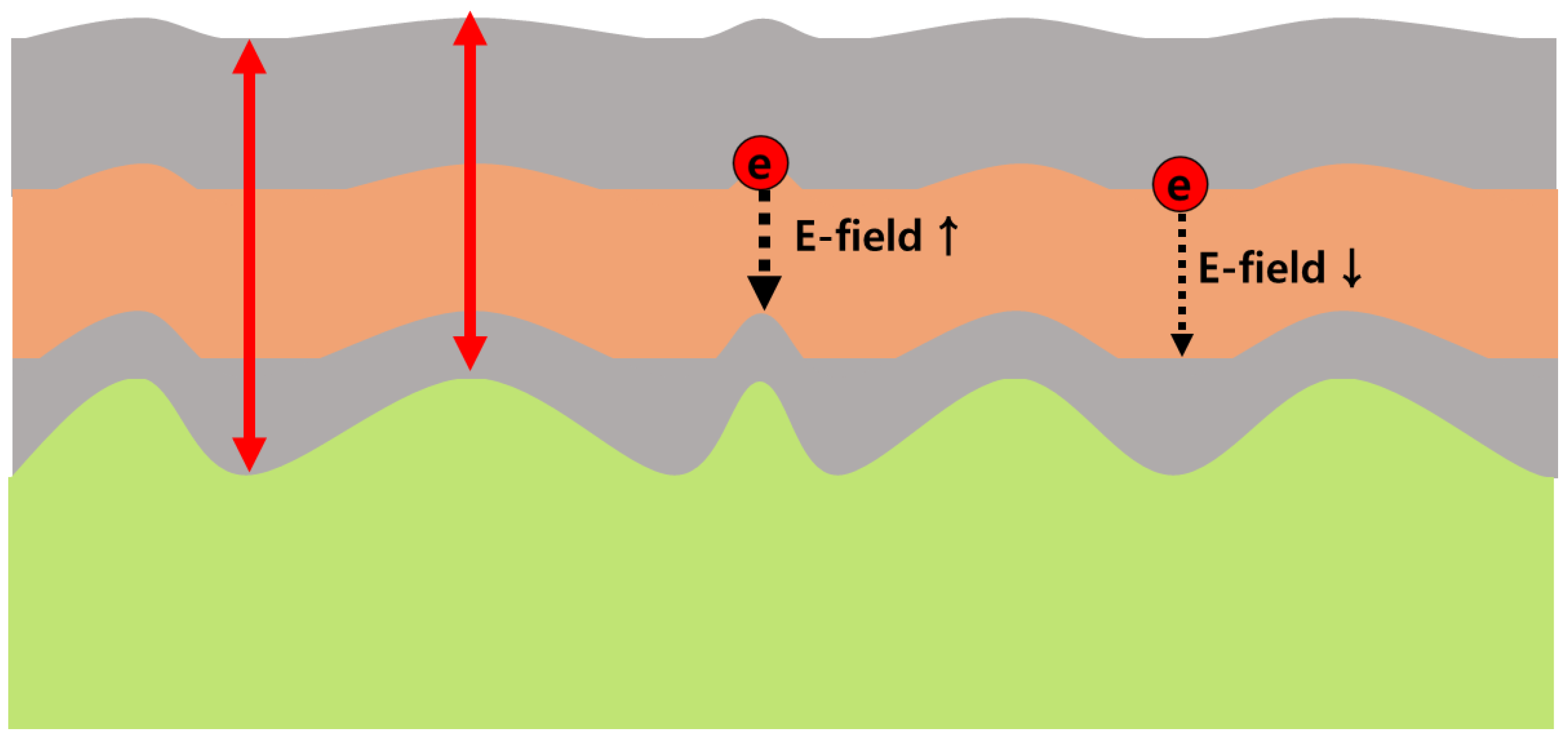
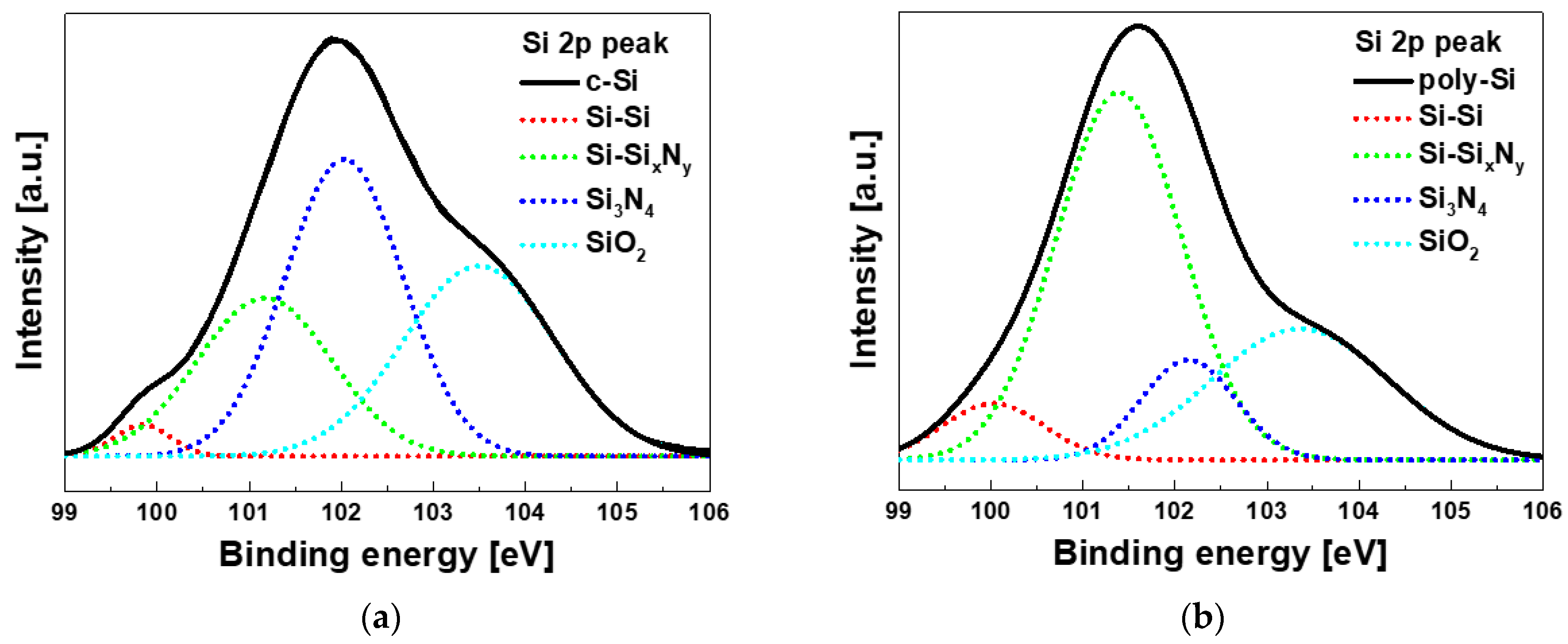
3.1. Physical Characteristic Analysis

AFM was used to compare the surface roughness of nitride-oxide (NO) stacked film on c-Si and poly-Si. Figure 2a,b shows the AFM images of NO on c-Si, poly-Si. As a reference, the surface roughness of poly-Si on Si substrate is presented in Figure 2c. From Figure 2a,b, it can be seen that Si3N4 has very rough surface on poly-Si. In Table 2, the extracted roughness values are summarized. From the results, it can be seen that the surface roughness of a film is affected by the underlayer.
From the AFM results, the cross section of the poly-Si device can be drawn as Figure 3, where the roughness of poly-Si causes poor coverage of TO and CTL resulting in the thickness and electric filed fluctuation in each layer. In this case, the electrical characteristics of device are deteriorated by the local increase of electric field in the thin area [12,13]. In addition, the interface roughness influences the interface defect formation by intensifying the lattice constant mismatch between the layers [14,15]. It is well known that the shallow interface traps between TO and CTL affects SONOS flash memory performance [16,17].

XPS Analysis

The depth profile analysis of XPS was performed to investigate the bonding structure of the TO and CTL interface according to the channel material change. Figure 4 shows the XPS multi-peak fitting results of Si 2p peak, which are corrected to 285.5 eV of C 1s. The Si 2p spectra can be fitted by 4 peaks using a Gaussian function. Si-Si peak is 99.9 ± 0.15 eV, Si-SixNy peak is 101.3 ± 0.15 eV, Si3N4 peak is 102.1 ± 0.1 eV, and SiO2 peak is 103.4 ± 0.1 eV [18,19]. Si-SixNy bonding represents a combination of Si3N4 that does not match the composition ratio. Table 3 shows the peak positions and ratios in each device. Ratio is the percentage of the area of each peak to the total area of the peak. The Si-Si and SiO2 ratios show similar percentages, but the SixNy and Si3N4 ratios show opposite results. The reason why the Si-SixNy bonding ratio is higher in poly-Si devices can be explained by the interface degradation as in AFM analysis. Si-SixNy bonding acts as trap in the CTL and affects the reliability of the memory.
Figure 5 shows the basic structure of Si3N4 and the trap model. In Si3N4, silicon vacancy (VSi) and nitrogen vacancy (VN) can be made, and their properties can be changed by atoms entering the vacancy. In general, interface traps have relatively shallower energy traps than bulk traps. As a characteristic of the SONOS structure, since the CTL is adjacent to the oxide layer, oxygen related defects may be formed by oxygen diffusion in the TO or BO. In particular, the bond by the O atom substituted with VN has a small energy level [20]. From the physical analysis, it was confirmed that the roughness deterioration of the underlayer formed more VSi and VN between the TO/BO and CTL, and the increase of the interface trap had a significant effect on the reliability of the memory [20,21,22].

3.2. Electrical Characteristic Analysis

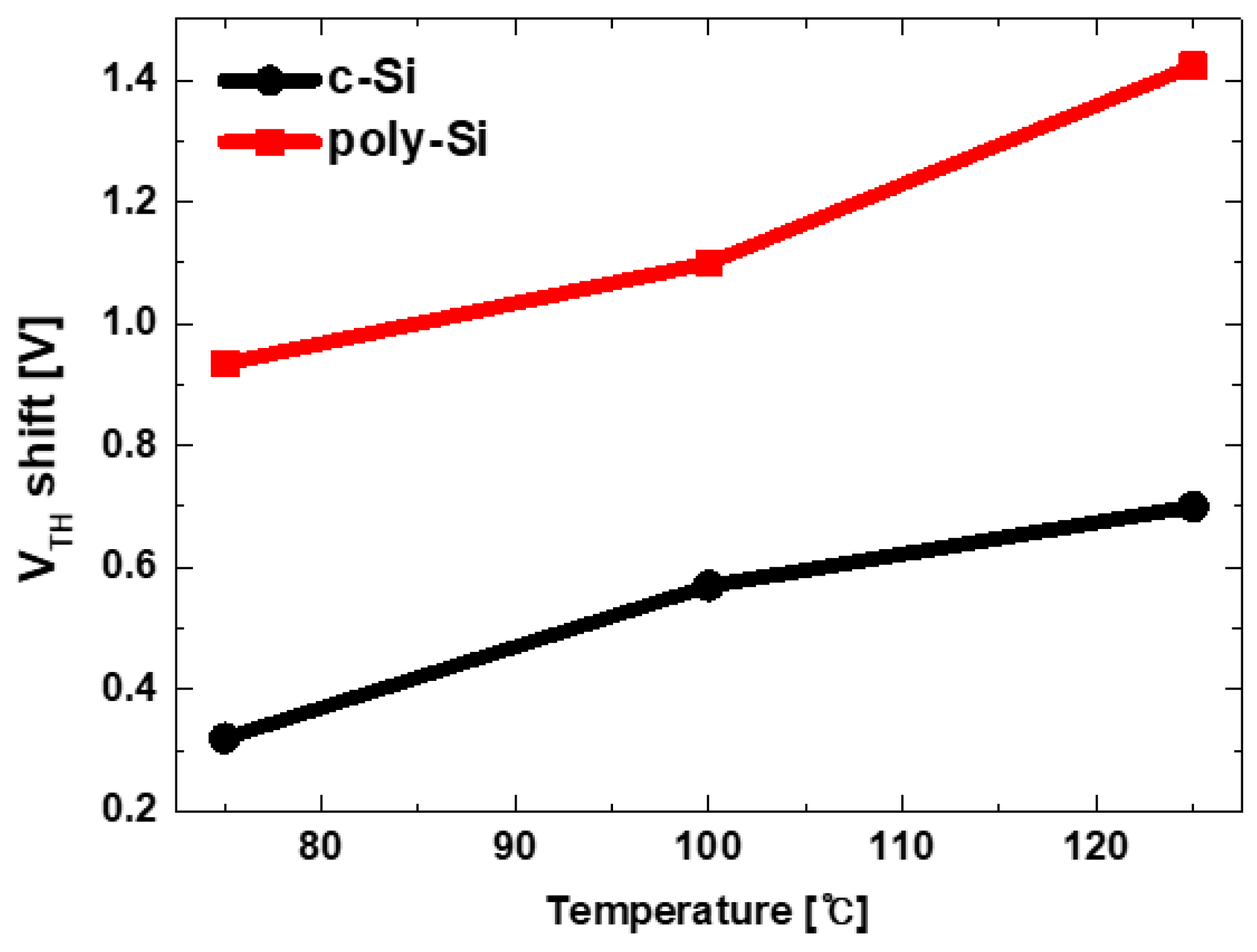
3.2.1. Data Retention Measurement

The program (PRG) and data retention behavior of the fabricated devices were measured as shown in Figure 6 and the charge loss in data retention mode was calculated. In data retention mode, C-V were measured after baking at 75~125 °C (25 °C step) for 1 h after programming. Poly-Si channel shows large program window (higher VTH shift) at the same program voltage than c-Si channel. However, larger VTH shift (ΔVTH) in the data retention meaning inferior reliability. Figure 7 shows ΔVTH in the data retention mode according to temperature. VTH was extracted as a gate voltage at 80% of the maximum capacitance. ΔVTH is much larger in all temperature conditions and the data retention characteristics are deteriorated in poly-Si devices. Considering shallow traps improves program windows with the traditional tradeoff in data retention properties, the experimental results show that more traps exist in the poly-Si channel device, which is same with the previous physical analysis.

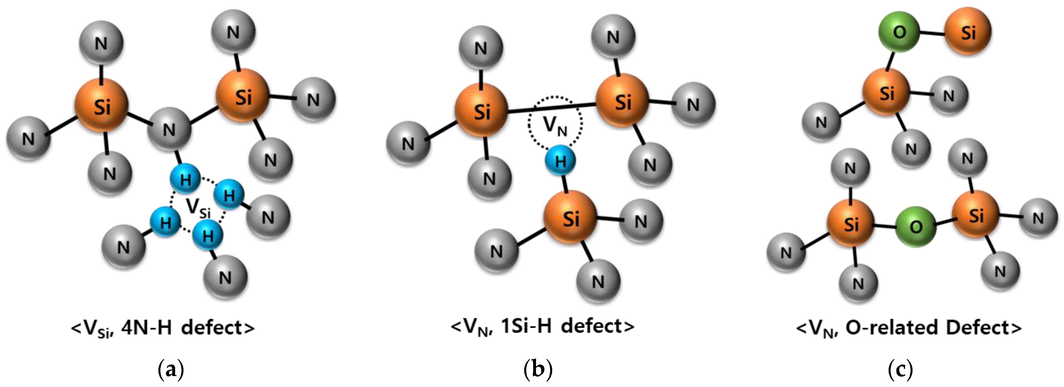
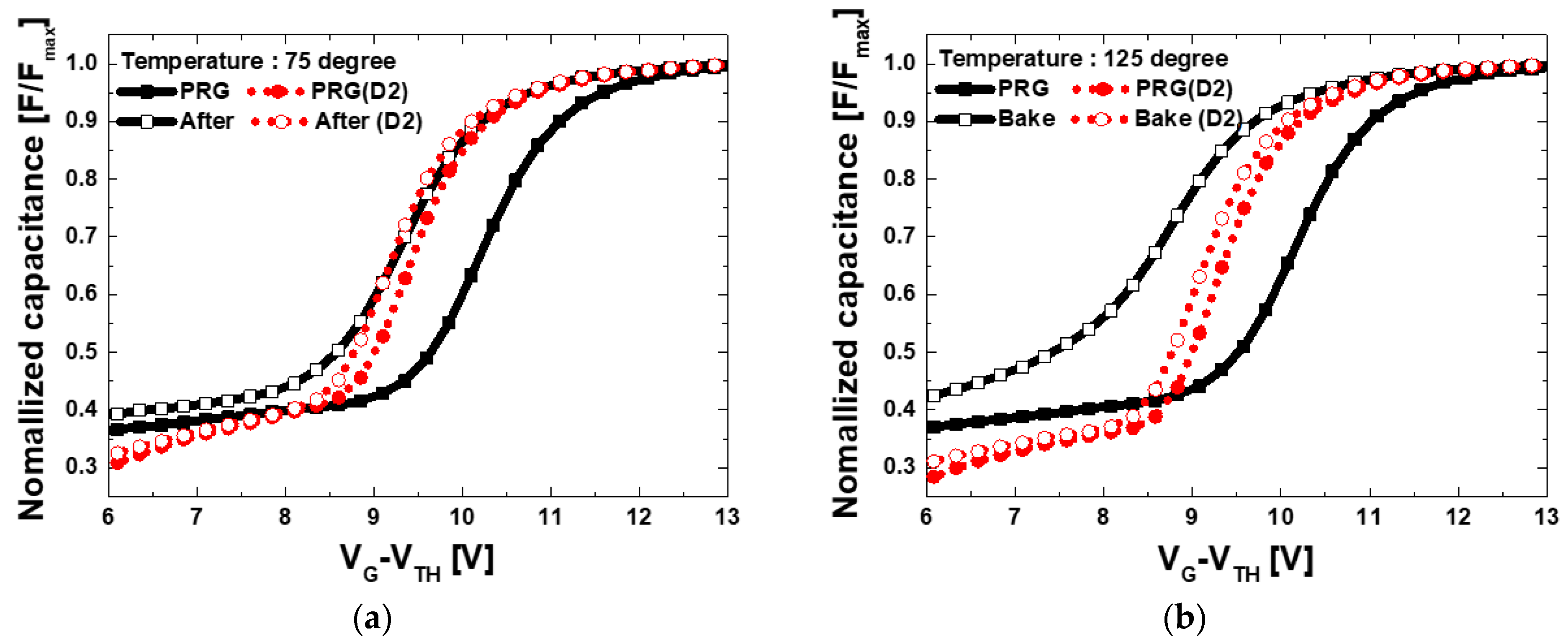
3.2.2. High Pressure D2 Annealing Effect

In this study, high pressure D2 annealing is suggested to make the device stable as a low temperature process method. Figure 8 shows trap models in Si3N4. Figure 8a shows 4N-H defect where hydrogen enters into VSi. This defect can be ignored because its energy level is not in the bandgap [23]. In Figure 8b, hydrogen enters into nitrogen vacancy (VN) and forms a 1Si-H defect and some Si-Si bonds [24,25]. Figure 8c shows O-related traps due to oxygen diffusion into VN [26], which is common near oxide film similar to TO/CTL or CTL/BO interface. In this experiment, to suppress O-related defects near TO/CTL or CTL/BO interface, passivation of VN is focused and high pressure D2 annealing is applied as stable curing method at low temperature.
Figure 9 shows the C-V data retention measurement results according to high pressure D2 annealing of a poly-Si channel device. Table 4 shows the VTH extracted according to the measurement temperature and high pressure D2 annealing. After D2 passivation through high pressure annealing, the memory window decreased, but the device reliability was greatly improved. These results are consistent with the previously predicted effect of shallow trap curing of Si3N4 by D2 annealing [27]. This result implies that even though the hydrogen can be dissociated during the post annealing period, some could form stable bondage with Si and N atoms. Furthermore, previous research had conducted D2 high pressure annealing even at 900 °C temperature [28].
For the physical analysis on the reduced shallow trap density, it is needed to detect the change in atomic bonding in Si3N4 by the deuterium bonding. FT-IR analysis can be employed for detecting and determining bond densities of light atoms such as H2 or D2 [29]. In this experiment, the results are not presented but Thermo-Nicolet 5700 FT-IR spectrometer is analyzed on the c-Si channel device with and without D2 treatment where the sample with D2 HPA with 600 °C annealing shows slightly increased absorbance in the rage of 2375 cm−1. It is difficult to detect the light atoms such as hydron quantitatively, more precise physical method should be studied.

4. Conclusions

In this study, the physical and electrical characteristics of the SONOS flash memory device with poly-Si channel were analyzed, and high pressure D2 annealing was suggested to improve the device performance. For physical analysis, surface roughness through AFM and trap of TO/CTL interface through XPS were analyzed. From the physical analysis, it was confirmed that underlaying poly-Si deteriorates the surface roughness of CTL and enlarges physical defects. For electrical analysis, ΔVTH was measured in data retention mode and larger in poly-Si devices as confirmed in the physical analysis. However, by high-pressure D2 annealing, the deteriorated memory characteristics can be improved. From the data retention measurement before and after D2 annealing, it was confirmed that the memory window slightly decreased due to the curing of the interface trap, but the ΔVTH significantly decreased. The results show a problem that appears when poly-Si channel is used in SONOS devices and indicate that high pressure D2 annealing is effective method to control the trap sites in interface of CTL.

Author Contributions

Methodology, formal analysis, investigation, writing—original draft, J.-K.J.; data curation, visualization, J.-Y.S., W.-S.K. and K.-R.N.; funding acquisition, resources, H.-D.L.; conceptualization, methodology, writing—review and editing, funding acquisition, supervision, G.-W.L. All authors have read and agreed to the published version of the manuscript.

Funding

This work was supported by the National Research Foundation of Korea (NRF) grant funded by the Korea government (MSIT) (NRF-2019M3F3A1A01074449, NRF-2019R1A2C1084717).

Data Availability Statement

Not applicable.

Conflicts of Interest

The authors declare no conflict of interest.

References

  1. Yang, S.D.; Oh, J.S.; Yun, H.J.; Jeong, K.S.; Kim, Y.M.; Lee, S.Y.; Lee, H.-D.; Lee, G.-W. The short channel effect immunity of silicon nanowire SONOS flash memory using TCAD simulation. Trans. Electr. Electron. Mater. 2013, 14, 139–142. [Google Scholar] [CrossRef]
  2. Xie, Q.; Lee, C.J.; Xu, J.; Wann, C.; Sun, J.Y.C.; Taur, Y. Comprehensive analysis of short-channel effects in ultrathin SOI MOSFETs. IEEE Trans. Electron. Devices 2013, 60, 1814–1819. [Google Scholar] [CrossRef]
  3. Bohara, P.; Vishvakarma, S.K. NAND flash memory device with ground plane in buried oxide for reduced short channel effects and improved data retention. J. Comput. Electron. 2019, 18, 500–508. [Google Scholar] [CrossRef]
  4. Endoh, T.; Kinoshita, K.; Tanigami, T.; Wada, Y.; Sato, K.; Yamada, K.; Yokoyama, T.; Takeuchi, N.; Tanaka, K.; Awaya, N.; et al. Novel ultrahigh-density flash memory with a stacked-surrounding gate transistor (S-SGT) structured cell. IEEE Trans. Electron. Devices 2003, 50, 945–951. [Google Scholar] [CrossRef]
  5. Kim, H.; Ahn, S.J.; Shin, Y.G.; Lee, K.; Jung, E. Evolution of NAND flash memory: From 2D to 3D as a storage market leader. In Proceedings of the 2017 IEEE International Memory Workshop (IMW), Monterey, CA, USA, 14–17 May 2017; IEEE: Monterey, CA, USA, 2017; pp. 1–4. [Google Scholar]
  6. Seager, C.H. Grain boundaries in polycrystalline silicon. Ann. Rev. Mater. Sci. 1985, 15, 271–302. [Google Scholar] [CrossRef]
  7. Yamashita, Y.; Asano, A.; Nishioka, Y.; Kobayashi, H. Dependence of interface states in the Si band gap on oxide atomic density and interfacial roughness. Phys. Rev. B 1999, 59, 15872. [Google Scholar] [CrossRef]
  8. Hong, S.B.; Park, J.H.; Lee, T.H.; Lim, J.H.; Shin, C.; Park, Y.W.; Kim, T.G. Variation of poly-Si grain structures under thermal annealing and its effect on the performance of TiN/Al2O3/Si3N4/SiO2/poly-Si capacitors. Appl. Surf. Sci. 2019, 477, 104–110. [Google Scholar] [CrossRef]
  9. Aozasa, H.; Fujiwara, I.; Nomoto, K.; Komatsu, H.; Koyama, K.; Kobayashi, T.; Oda, T. Effects of nitridation on the electrical properties of MONOS nonvolatile memories. J. Electrochem. Soc. 2007, 154, H798. [Google Scholar] [CrossRef]
  10. Kizilyalli, I.C.; Lyding, J.W.; Hess, K. Deuterium post-metal annealing of MOSFET’s for improved hot carrier reliability. IEEE Electron. Device Lett. 1997, 18, 81–83. [Google Scholar] [CrossRef]
  11. Cheng, K.; Hess, K.; Lyding, J.W. A new technique to quantify deuterium passivation of interface traps in MOS devices. IEEE Electron. Device Lett. 2001, 22, 203–205. [Google Scholar] [CrossRef]
  12. Yang, Y.L.; Purwar, A.; White, M.H. Reliability considerations in scaled SONOS nonvolatile memory devices. Solid State Electron. 1999, 43, 2025–2032. [Google Scholar] [CrossRef]
  13. Li, W.; Li, D.Y. On the correlation between surface roughness and work function in copper. J. Chem. Phys. 2005, 122, 064708. [Google Scholar] [CrossRef] [PubMed]
  14. Choi, Y.W.; Xie, K.; Kim, H.M.; Wie, C.R. Interface trap and interface depletion in lattice-mismatched GaInAs/GaAs heterostructures. J. Electron. Mater. 1991, 20, 545–551. [Google Scholar] [CrossRef]
  15. Huang, Z.C.; Wie, C.R.; Johnstone, D.K.; Stutz, C.E.; Evans, K.R. Effects of lattice mismatch and thermal annealing on deep traps and interface states in Ga0. 92In0. 08As (n+)/GaAs (p) heterojunctions. J. Appl. Phys. 1993, 73, 4362–4366. [Google Scholar] [CrossRef]
  16. Lee, J.D.; Choi, J.H.; Park, D.; Kim, K. Effects of interface trap generation and annihilation on the data retention characteristics of flash memory cells. IEEE Trans. Device Mater. Reliab. 2004, 4, 110–117. [Google Scholar] [CrossRef]
  17. Yang, S.D.; Jung, J.K.; Lim, J.G.; Park, S.G.; Lee, H.D.; Lee, G.W. Investigation of Intra-Nitride Charge Migration Suppression in SONOS Flash Memory. Micromachines 2019, 10, 356. [Google Scholar] [CrossRef] [PubMed] [Green Version]
  18. Park, Y.B.; Rhee, S.W. Bulk and interface properties of low-temperature silicon nitride films deposited by remote plasma enhanced chemical vapor deposition. J. Mater. Sci. Mater. Electron. 2001, 12, 515–522. [Google Scholar] [CrossRef]
  19. Huang, J.J.; Liu, C.J.; Lin, H.C.; Tsai, C.J.; Chen, Y.P.; Hu, G.R.; Lee, C.C. Influences of low temperature silicon nitride films on the electrical performances of hydrogenated amorphous silicon thin film transistors. J. Phys. D Appl. Phys. 2008, 41, 245502. [Google Scholar] [CrossRef]
  20. Wong, H.; Gritsenko, V.A. Defects in silicon oxynitride gate dielectric films. Microelectron. Reliab. 2002, 42, 597–605. [Google Scholar] [CrossRef]
  21. Lusky, E.; Shacham-Diamand, Y.; Shappir, A.; Bloom, I.; Eitan, B. Traps spectroscopy of the Si3Ni4 layer using localized charge-trapping nonvolatile memory device. Appl. Phys. Lett. 2004, 85, 669–671. [Google Scholar] [CrossRef]
  22. Perera, R.; Ikeda, A.; Hattori, R.; Kuroki, Y. Effects of post annealing on removal of defect states in silicon oxynitride films grown by oxidation of silicon substrates nitrided in inductively coupled nitrogen plasma. Thin Solid Film 2003, 423, 212–217. [Google Scholar] [CrossRef]
  23. Vianello, E.; Driussi, F.; Blaise, P.; Palestri, P.; Esseni, D.; Perniola, L.; Molas, G.; De Salvo, B.; Selmi, L. Explanation of the charge trapping properties of silicon nitride storage layers for NVMs—Part II: Atomistic and electrical modeling. IEEE Trans. Electron. Devices 2011, 58, 2490–2499. [Google Scholar] [CrossRef] [Green Version]
  24. Gritsenko, V.A.; Perevalov, T.V.; Orlov, O.M.; Krasnikov, G.Y. Nature of traps responsible for the memory effect in silicon nitride. Appl. Phys. Lett. 2016, 109, 062904. [Google Scholar] [CrossRef]
  25. Sonoda, K.I.; Tsukuda, E.; Tanizawa, M.; Yamaguchi, Y. Electron trap level of hydrogen incorporated nitrogen vacancies in silicon nitride. J. Appl. Phys. 2015, 117, 104501. [Google Scholar] [CrossRef]
  26. Yamaguchi, K.; Otake, A.; Kobayashi, K.; Shiraishi, K. Atomistic guiding principles for MONOS-type memories with high program/erase cycle endurance. In Proceedings of the 2009 IEEE International Electron Devices Meeting (IEDM), Baltimore, MD, USA, 7–9 December 2009; IEEE: Baltimore, MD, USA, 2009; pp. 1–4. [Google Scholar]
  27. Noguchi, M.; Isogai, T.; Yamashita, H.; Sawa, K.; Fujitsuka, R.; Yamanaka, T.; Okada, S.; Aoyama, T.; Aiso, F.; Abe, J.; et al. Formation of High Reliability Hydrogen-free MONOS Cells Using Deuterated Ammonia. In Proceedings of the 2019 IEEE International Electron Devices Meeting (IEDM), San Francisco, CA, USA, 7–11 December 2019; IEEE: San Francisco, CA, USA, 2019; pp. 30–32. [Google Scholar]
  28. Tanaka, M.; Saida, S.; Mitani, Y.; Mizushima, I.; Tsunashima, Y. Highly reliable MONOS Devices with optimized silicon nitride film having deuterium terminated charge traps. In Proceedings of the 2002 Digest. International Electron Devices Meeting, Washington, DC, USA, 2–5 December 2001; IEEE: San Francisco, CA, USA, 2003; pp. 237–240. [Google Scholar]
  29. Choi, S.; Baek, S.; Jang, M.; Jeon, S.; Kim, J.; Kim, C.; Hwang, H. Effects of High-Pressure Deuterium annealing on nonvolatile memory device with silicon nanocrystals embedded in silicon nitride. J. Electrochem. Soc. 2005, 152, G345. [Google Scholar] [CrossRef]
Figure 1. (a) The structures of a c-Si and poly-Si SONOS type capacitor devices, and (b) the process flow of the device fabrication.
Micromachines 12 01401 g001
Figure 2. AFM images of fabricated devices in a square region about 5 μm/5 μm. The device structures are (a) NO on c-Si, (b) NO on poly-Si, and (c) only poly-Si deposited on Si substrate, respectively.
Micromachines 12 01401 g002
Figure 3. Schematic cross section of a SONOS transistors with poly-Si channel. The roughness of poly-Si causes poor coverage of tunneling oxide and nitride resulting in large electric field fluctuation in each layer.
Micromachines 12 01401 g003
Figure 4. X-ray Photoelectron Spectroscopy (XPS) results of Si 2p multi peak fitting of tunneling oxide/charge trapping layer interface on (a) c-Si and (b) poly-Si channel device.
Micromachines 12 01401 g004
Figure 5. (a) Standard structure of the crystal Si3N4. Main defects (b) silicon vacancy and (c) nitrogen vacancy.
Micromachines 12 01401 g005
Figure 6. Measurement result of program and data retention characteristics of the fabricated devices. Here, the retention properties were measured after baking at 75~125 °C for 1 h.
Micromachines 12 01401 g006
Figure 7. ΔVTH of c-Si and poly-Si channel devices in data retention mode according to the temperature.
Micromachines 12 01401 g007
Figure 8. Trap model that can appear in the TO/CTL interface after high pressure D2 annealing. (a) VSi with substitutional H atom at Si site, (b) VN with substitutional H atom at N site or Si-Si bond form, and (c) VN with substitutional O atom at N site.
Micromachines 12 01401 g008
Figure 9. The result of measuring the program and data retention characteristics of the manufactured device according to the high pressure D2 annealing of the poly-Si channel device. Data retention measurement temperature (a) 75 °C and (b) 125 °C.
Micromachines 12 01401 g009
Table 1. Process conditions of SiO2 (BO or TO) and Si3N4 (CTL) deposited by LPCVD.
LPCVDTemperature (°C)Pressure (mTorr)Composition Ratio
SiO2800-Si(OC2H5)4
Si3N4720200SiH2Cl2:NH3 = 20:120
Table 2. AFM analysis results on surface roughness of NO stacked film on c-Si and poly-Si. In addition, poly-Si roughness is also measured for a reference which is expressed as “Only poly-Si” sample.
ConditionPeak to Valley (nm)Mean Height (nm)RMS Roughness (nm)
c-Si channel1.200.157
Poly-Si channel15.7150.4942.422
Only poly-Si12.6270.1582.660
Table 3. Extraction results of Si 2p peak parameters according to underlaying channel material.
c-SiSi-SiSixNySi3N4SiO2poly-SiSi-SiSixNySi3N4SiO2
Peak (eV)99.84101.17102.03103.49Peak (eV)100.02101.39102.14103.36
Ratio (%)2254033Ratio (%)7541128
Table 4. Extracted VTH based on data retention measurement according to temperature and high pressure D2 annealing.
Temperature (°C)75125
ConditionNo TreatmentD2 AnnealingNo TreatmentD2 Annealing
Program (V)10.759.8610.589.74
Bake (V)9.829.689.169.54
ΔVTH (V)0.930.181.420.20
Publisher’s Note: MDPI stays neutral with regard to jurisdictional claims in published maps and institutional affiliations.

