Article

Fabrication and Characterization of Nanonet-Channel LTPS TFTs Using a Nanosphere-Assisted Patterning Technique

1
Department of Electrical Engineering, Pohang University of Science and Technology, Pohang 37673, Korea
2
Division of IT Convergence Engineering, Pohang University of Science and Technology, Pohang 37673, Korea
*
Authors to whom correspondence should be addressed.
Micromachines 2021, 12(7), 741; https://doi.org/10.3390/mi12070741
Submission received: 20 May 2021 / Revised: 20 June 2021 / Accepted: 20 June 2021 / Published: 24 June 2021
(This article belongs to the Special Issue Thin Film Transistors: Material, Structure and Application)

Abstract

:
We present the fabrication and electrical characteristics of nanonet-channel (NET) low-temperature polysilicon channel (LTPS) thin-film transistors (TFTs) using a nanosphere-assisted patterning (NAP) technique. The NAP technique is introduced to form a nanonet-channel instead of the electron beam lithography (EBL) or conventional photolithography method. The size and space of the holes in the nanonet structure are well controlled by oxygen plasma treatment and a metal lift-off process. The nanonet-channel TFTs show improved electrical characteristics in terms of the ION/IOFF, threshold voltage, and subthreshold swing compared with conventional planar devices. The nanonet-channel devices also show a high immunity to hot-carrier injection and a lower variation of electrical characteristics. The standard deviation of VTH (σVTH) is reduced by 33% for a nanonet-channel device with a gate length of 3 μm, which is mainly attributed to the reduction of the grain boundary traps and enhanced gate controllability. These results suggest that the cost-effective NAP technique is promising for manufacturing high-performance nanonet-channel LTPS TFTs with lower electrical variations.

Graphical Abstract

1. Introduction

Polysilicon thin-film transistors (poly-Si TFTs) have been widely used in flat panel displays, image sensors, and 3D memory devices [1,2,3,4,5,6,7,8,9,10]. However, the inherent grain boundary (GB) in the poly-Si layer can significantly affect the electrical behaviors and reliability characteristics. The acceptor-like or donor-like traps in GBs can cause potential-barrier fluctuations and interrupt the carrier flow in the channel [11,12]. Another important issue is the non-uniformity of the electrical performance caused by the size, number, and quality of GBs varied from device to device and wafer to wafer [13,14]. In order to mitigate the effect of GB traps, a thermal post-annealing process and a modulated excimer-laser method were reported [15,16,17,18,19].
Recently, a macaroni channel structure demonstrated an improved performance for 3D memory devices. The core poly-Si channel was etched out and filled with a dielectric. The improved performance was mainly due to the reduced GB traps and the effect of the thin-body channel [20]. More recently, nanonet-channel TFTs were successfully demonstrated. Hexagonal holes with various pattern sizes and distances between patterns were formed in the poly-Si channel region using electron beam lithography (EBL). As a result of the effective reduction of grain boundary traps and enhanced gate controllability, the nanonet-channel TFTs showed a better subthreshold swing (SS), lower threshold voltage (VTH), and higher ON-OFF current ratio (ION/IOFF) compared with conventional planar TFTs [21,22]. However, for large-area applications of nanonet-channel devices, an alternative lithography method with a relatively cheap and high through-put is inevitably required.
Here, a nanosphere-assisted patterning (NAP) technique involving oxygen plasma treatment has been developed to form the nanonet structure. The NAP technique with the advantages of inexpensive equipment and the capability of large-area patterning, has been widely used to realize periodic photonic devices [23,24], solar cell [25], biological devices [26,27], and electrical sensors [28,29].
We demonstrated nanonet-channel low-temperature polysilicon (LTPS) thin-film transistors (TFTs) using the NAP technique. The DC performance and reliability were characterized and compared with those of conventional planar devices. The impact of the nanonet-channel on the variation of electrical characteristics was also investigated.

2. Experimental Details

Nanonet-channel LTPS TFTs (NET_TFTs) and conventional planar TFTs (CON_TFTs) were fabricated on an LTPS-on-glass substrate. The LTPS was prepared by depositing an amorphous Si using a low-pressure chemical vapor deposition (LPCVD) at 550 °C and a subsequent excimer laser annealing (ELA) process. The grain size and thickness of the poly-Si were about 200–400 nm and 50 nm, respectively [21,22]. Both devices underwent the same process steps, except for the nanonet structure formation processes. Figure 1 shows a schematic diagram of the process flow of the nanonet-channel devices using the NAP technique. First, a mask aligner and an inductively coupled plasma (ICP) dry etcher were used to define the source and drain (S/D) regions (Figure 1a). Next, a 20-nm SiO2 isolation layer was deposited by plasma-enhanced chemical vapor deposition (PECVD) (Figure 1b). A monolayer of polystyrene nanospheres (PNs) was uniformly formed on the isolation layer by a spin coating process, and then, the O2 plasma treatment was performed to control the size of the PNs (Figure 1c,d). Then, a perforated metal film with a nanohole pattern was formed by a lift-off process. A hard mask was formed on the S/D region using a mask aligner, and the isolation layer and LTPS were etched using an ICP etcher. All of the hard mask layers were then removed (Figure 1e–g). Next, a 100-nm SiO2 gate oxide layer was deposited using PECVD, and Mo was deposited as a gate electrode, followed by patterning using an ICP etcher. Next, the S/D regions were implanted with phosphorus (20 keV at 2 × 1015 cm−2), and rapid thermal annealing was performed (Figure 1h). Finally, Ti/Ag (500 nm/2000 nm) interconnection metal films were deposited and forming gas annealing was performed at 450 °C for 30 min.
Figure 2 shows the dependence of the diameter of the PNs on the O2 plasma treatment. The plasma parameters used were an RF power of 50 W, O2 flow rate of 50 sccm, and chamber pressure of 450 mTorr. The nanosphere size was adjusted by increasing the O2 plasma etching time. The diameter of the PNs decreased slowly and then rapidly after 1 min of etching time, which can determine the hole pattern size (WH) and distance between patterns (WD) in the nanonet-channel region. The plasma treatment time of 85 s was used to form the reproducible nanonet structures.
Both the NET_TFTs and CON_TFTs had gate lengths (LGATE) of 3, 6, or 10 μm and a width (WGATE) of 5 μm. In the NET_TFTs, the hole size (WH) and the distance between holes (WD) in the nanonet-channel region were fixed at 320 nm and 130 nm, respectively. The electrical characteristics and hot-carrier injection (HCI) were measured using a semiconductor parameter analyzer (Keithley 4200).

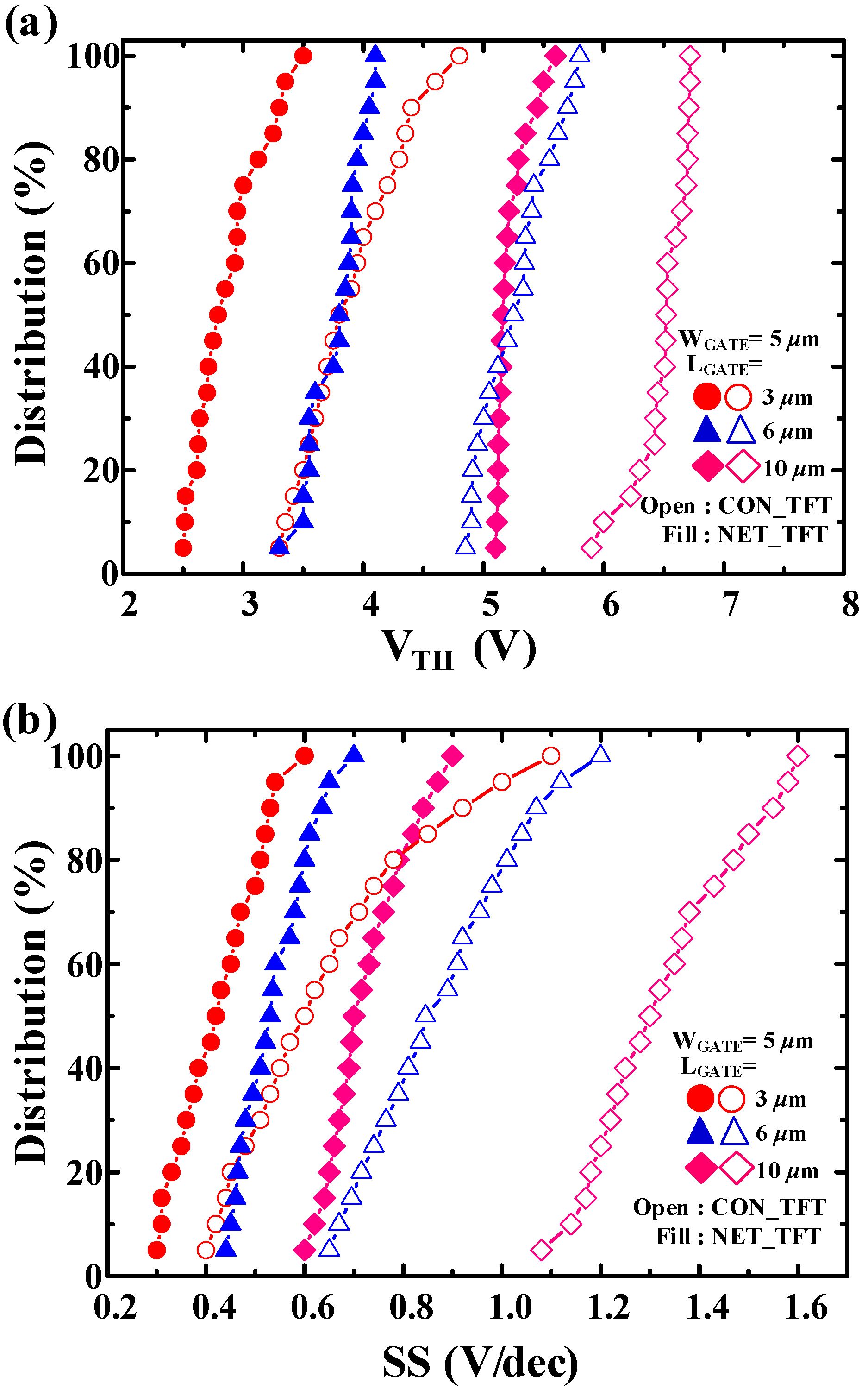
3. Results and Discussions

Figure 3a shows the scanning electron microscope (SEM) images of the spin-coated PNs on the substrate, where 450-nm PNs are uniformly arranged. After the NAP process (Figure 1g), nanonet patterns were successfully formed onto the LTPS layer with a WH of 320 nm and WD of 130 nm, as shown in Figure 3b.
The initial channel volume (WGATE × LGATE × Tsi) was the same in both CON_TFTs and NET_TFTs, as shown in Figure 4. The threshold voltage (VTH_CON) was dependent on the total number of traps related to the channel volume, as follows [20]:
V T H _ C O N V F B + 2 F + q N t r a p C O X ( W G A T E · L G A T E ) · T s i
where q is the electric charge, COX is the gate-oxide capacitance, Ntrap is the total number of traps per unit volume, and Tsi is the channel thickness.
The lowering of the threshold voltage (VTH_NET) using the nanonet channel is described as follows:
V T H _ N E T V F B + 2 F + q N t r a p C O X ( W G A T E · L G A T E N H · π R H ) · T s i
where NH is a number of holes in the nanonet channel and RH is a diameter of the hole.
Compared with the planar device, the nanonet-channel device can lower the threshold voltage by decreasing the total traps. Furthermore, the tri-gate effect between the holes in the nanonet channel can improve the electrical characteristics as a result of the enhanced gate controllability [21,22,30].
Figure 5 shows the measured DC characteristics of both NET_TFTs and CON_TFTs at room temperature. The ON-state current (ION) and the OFF-state minimum leakage current (IOFF) were measured at VG − VTH = 3 V and −5 V with VD = 1 V, respectively. The threshold voltage was extracted using the linear extrapolation method [31]. The subthreshold slope was calculated as [ d ( log 10 I D ) / d V G ] 1 . As LGATE decreased, both devices showed an improved performance mainly due to the lower GB traps at shorter channel lengths [32]. Compared with the CON_TFTs, NET_TFTs showed a higher ION/IOFF and μ*FE, and lower SS and VTH, which was similar to previous results obtained using EBL technique [21,22]. The mean drain-induced barrier lowering (DIBL) with LGATE = 3 μm was 130 mV/V for NET_TFTs and 230 mV/V for CON_TFTs, respectively. The mean μ*FE (≡μFE × WGATE/LGATE = gm⋅(COX⋅VD)−1) [21] and ION/IOFF of the NET_TFTs increased by ~18% and ~120% from LGATE = 10 μm to LGATE = 3 μm, respectively.
At LGATE = 3 μm, the mean SS and VTH of NET_TFTs were ~33% and 25% lower, respectively, than those of CON_TFTs. Moreover, for all of the channels, the NET_TFTs had a higher ION/IOFF and μ*FE, improved SS, and lower VTH compared with CON_TFTs.
The grain boundary trap density (NGB) and interface trap density (NIT) were extracted to verify the influence of the nanonet-channel structure on the trap level in the poly-Si channel [32,33,34,35]. At LGATE = 3 μm and WH = 320 nm, the extracted NGB and NIT values were 9.8 × 1011 cm2 and 1.7 × 1012 cm2 for CON_TFT, and 5.4 × 1011 cm2 and 1.01 × 1012 cm2 for NET_TFT, respectively. As a result of the enhanced gate controllability and effective reduction of GB traps, NET_TFTs could provide a better interface quality and improved electrical characteristics [21,22]. Figure 6 shows the degradation of VTH and SS under HCI conditions at VG − VTH = VD = 4 V. The degradation is generally caused by trap-generation in GBs and at the oxide/channel interface under HC stress conditions [36]. Similar to previous results, NET_TFTs showed a higher immunity to HCI stress than CON_TFTs because of the effective reduction of GB traps in the nanonet-channel [21].
The variation of the electrical characteristics of both devices were investigated at room temperature. Figure 7 shows the cumulative distribution of SS and VTH for NET_TFTs and CON_TFTs with LGATE = 3, 6, and 10 μm. The NET_TFTs showed lower variation compared with the CON_TFTs. The average and standard deviation of SS and VTH are shown in Table 1. As LGATE decreased, the standard deviation increased slightly for both devices, which is consistent with the results that the variation of electrical characteristics increased as the device shrank.
Figure 8 shows the standard deviation of VTH (σVTH) for both devices as a function of the device area ((LW)−1/2). σVTH can be expressed as follows [37]:
σ V T H = q C O X N E F F W d e p 3 L W
where NEFF is the effective concentration of channel doping, Wdep is the depletion width of the channel, L is the footprint length, and W (=5 μm) is the foot-print width.
As shown in Figure 8, σVTH is clearly proportional to ( L W ) 1 / 2 . The slope of the linear-regression line for NET_TFTs is lower than that of CON_TFTs. NEFF and Wdep are largely affected by the presence of GB traps. Thus, in the nanonet-channel structure, the effective reduction of GB traps and better gate controllability can lead to a thinner Wdep and lower NEFF. These results suggest that the nanonet-channel is very effective for reducing the variation of the device characteristics.

4. Conclusions

We successfully fabricated nanonet-channel LTPS TFTs using the NAP technique involving oxygen plasma treatment. The nanonet-channel TFTs demonstrated a lower SS and VTH, higher ON/OFF current ratio, and a high immunity to hot carrier stress. Moreover, the nanonet-channel devices achieved a lowered variation of electrical characteristics, which was mainly attributed to the effective reduction of GB traps and enhanced gate controllability. These results indicate that the nanonet-channel TFTs using the NAP technology could be a promising solution for realizing mass production of high-performance TFT applications with a lower electrical variation.

Author Contributions

Conceptualization, G.Y. and I.P.; investigation, D.K.; methodology, D.K.; Data curation, B.J.; writing—original draft preparation, G.Y., B.J. and J.-S.L.; writing—review & editing, G.Y. and J.-S.L.; supervision, J.-S.L. All authors have read and agreed to the published version of the manuscript.

Funding

This work was supported by the Korea Institute of Planning and Evaluation for Technology in Foog, Agriculture, Forestry, and Fisheries (IPET) through the Animal Disease Management Technology Develop-ment Program, which is funded by the Ministry of Agriculture, Food, and Rural Affairs (MAFRA)(120091-02-1-CG000) and by the Future Semiconductor Device Technology Development Program (10067739) funded by Ministry of Trade, Industry & Energy (MOTIE) and Korea Semiconductor Rsearch Consortium (KSRC).

Conflicts of Interest

The authors declare that they have no conflict of interest.

References

  1. Tai, Y.-H.; Kuo, Y.-F.; Lee, Y.-H. Photosensitivity Analysis of Low-Temperature Poly-Si Thin-Film Transistor Based on the Unit-Lux-Current. IEEE Trans. Electron. Devices 2009, 56, 50–56. [Google Scholar] [CrossRef]
  2. Shih-Ching, C.; Ting-Chang, C.; Po-Tsun, L.; Yung-Chun, W.; Po-Shun, L.; Bae-Heng, T.; Jang-Hung, S.; Sze, S.M.; Chun-Yen, C.; Chen-Hsin, L. A Novel Nanowire Channel Poly-Si TFT Functioning as Transistor and Nonvolatile SONOS Memory. IEEE Electron. Device Lett. 2007, 28, 809–811. [Google Scholar] [CrossRef]
  3. Goto, T.; Saito, K.; Imaizumi, F.; Hatanaka, M.; Takimoto, M.; Mizumura, M.; Gotoh, J.; Ikenoue, H.; Sugawa, S. LTPS Thin-Film Transistors Fabricated Using New Selective Laser Annealing System. IEEE Trans. Electron. Devices 2018, 65, 3250–3256. [Google Scholar] [CrossRef]
  4. Asano, A.; Kinoshita, T. 43.2: Low-Temperature Polycrystalline-Silicon TFT Color LCD Panel Made of Plastic Substrates. SID Symp. Dig. Tech. Pap. 2002, 33, 1196. [Google Scholar] [CrossRef]
  5. Farmakis, F.V.; Brini, J.; Kamarinos, G.; Angelis, C.T.; Dimitriadis, C.A.; Miyasaka, M. On-current modeling of large-grain polycrystalline silicon thin-film transistors. IEEE Trans. Electron. Devices 2001, 48, 701–706. [Google Scholar] [CrossRef]
  6. Tsai, C.-C.; Wei, K.-F.; Lee, Y.-J.; Chen, H.-H.; Wang, J.-L.; Lee, I.-C.; Cheng, H.-C. High-Performance Short-Channel Double-Gate Low-Temperature Polysilicon Thin-Film Transistors Using Excimer Laser Crystallization. IEEE Electron. Device Lett. 2007, 28, 1010–1013. [Google Scholar] [CrossRef]
  7. Nakajima, Y.; Kida, Y.; Murase, M.; Toyoshima, Y.; Maki, Y. 21.3: Invited Paper: Latest Development of “System-on-Glass” Display with Low Temperature Poly-Si TFT. SID Symp. Dig. Tech. Pap. 2004, 35, 864. [Google Scholar] [CrossRef]
  8. Stewart, M.; Howell, R.S.; Pires, L.; Hatalis, M.K. Polysilicon TFT technology for active matrix OLED displays. IEEE Trans. Electron. Devices 2001, 48, 845–851. [Google Scholar] [CrossRef]
  9. Son, S.W.; Byun, C.W.; Lee, Y.W.; Yun, S.J.; Takaloo, A.V.; Park, J.H.; Joo, S.K. Effect of Dopant Concentration in Lightly Doped Drain Region on the Electrical Properties of N-Type Metal Induced Lateral Crystallization Polycrystalline Silicon Thin Film Transistors. Jpn. J. Appl. Phys. 2013, 52, 10MC13. [Google Scholar] [CrossRef]
  10. Park, J.H.; Seok, K.H.; Kim, H.Y.; Chae, H.J.; Lee, S.K.; Joo, S.K. A Novel Design of Quasi-Lightly Doped Drain Poly-Si Thin-Film Transistors for Suppression of Kink and Gate-Induced Drain Leakage Current. IEEE Electron. Device Lett. 2015, 36, 351–353. [Google Scholar] [CrossRef]
  11. Yamauchi, N.; Hajjar, J.-J.J.; Reif, R. Polysilicon thin-film transistors with channel length and width comparable to or smaller than the grain size of the thin film. IEEE Trans. Electron. Devices 1991, 38, 55–60. [Google Scholar] [CrossRef]
  12. Watakabe, H.; Sameshima, T. Polycrystalline silicon thin-film transistors fabricated by defect reduction methods. IEEE Trans. Electron. Devices 2002, 49, 2217–2221. [Google Scholar] [CrossRef]
  13. Wang, A.W.; Saraswat, K.C. A strategy for modeling of variations due to grain size in polycrystalline thin-film transistors. IEEE Trans. Electron. Devices 2000, 47, 1035–1043. [Google Scholar] [CrossRef]
  14. Kouvatsos, D.N.; Voutsas, A.T.; Hatalis, M.K. High-performance thin-film transistors in large grain size polysilicon deposited by thermal decomposition of disilane. IEEE Trans. Electron. Devices 1996, 43, 1399–1406. [Google Scholar] [CrossRef]
  15. Wu, I.-W.; Huang, T.-Y.; Jackson, W.B.; Lewis, A.G.; Chiang, A. Passivation kinetics of two types of defects in polysilicon TFT by plasma hydrogenation. IEEE Electron. Device Lett. 1991, 12, 181–183. [Google Scholar] [CrossRef]
  16. Chang-Ho, O.; Matsumura, M. A proposed single grain-boundary thin-film transistor. IEEE Electron. Device Lett. 2001, 22, 20–22. [Google Scholar] [CrossRef]
  17. Yeh, M.-S.; Lee, Y.-J.; Hung, M.-F.; Liu, K.-C.; Wu, Y.-C. High-Performance Gate-All-Around Poly-Si Thin-Film Transistors by Microwave Annealing with NH3 Plasma Passivation. IEEE Trans. Nanotechnol. 2013, 12, 636–640. [Google Scholar] [CrossRef]
  18. Sposili, R.S.; Im, J.S. Sequential lateral solidification of thin silicon films on SiO2. Appl. Phys. Lett. 1996, 69, 2864–2866. [Google Scholar] [CrossRef]
  19. Wang, C.-L.; Lee, I.-C.; Wu, C.-Y.; Chou, C.-H.; Yang, P.-Y.; Cheng, Y.-T.; Cheng, H.-C. High-Performance Polycrystalline-Silicon Nanowire Thin-Film Transistors with Location-Controlled Grain Boundary via Excimer Laser Crystallization. IEEE Electron. Device Lett. 2012, 33, 1562–1564. [Google Scholar] [CrossRef]
  20. Fukuzumi, Y.; Katsumata, R.; Kito, M.; Kido, M.; Sato, M.; Tanaka, H.; Nagata, Y.; Matsuoka, Y.; Iwata, Y.; Aochi, H.; et al. Optimal Integration and Characteristics of Vertical Array Devices for Ultra-High Density, Bit-Cost Scalable Flash Memory. In Proceedings of the 2007 International Electron Devices Meeting, Washington, DC, USA, 10–12 December 2007; pp. 449–452. [Google Scholar]
  21. Lee, H.; Lee, J.; Baek, S.; Jeong, W.H.; Lee, Y.; Yang, T.; Lee, J.-S. Highly Enhanced Performance of Network Channel Polysilicon Thin-Film Transistors. IEEE Electron. Device Lett. 2017, 38, 187–190. [Google Scholar] [CrossRef]
  22. Lee, J.; Lee, H.; Jin, B.; Oh, H.; Baek, S.; Yoon, G.; Lee, Y.; Baek, R.-H.; Lee, J.-S. Impact of geometrical parameters on the electrical performance of network-channel polycrystalline silicon thin-film transistors. Jpn. J. Appl. Phys. 2018, 57, 104001. [Google Scholar] [CrossRef]
  23. Liou, J.-K.; Chen, C.-C.; Chou, P.-C.; Tsai, Z.-J.; Chang, Y.-C.; Liu, W.-C. Implementation of a High-Performance GaN-Based Light-Emitting Diode Grown on a Nanocomb-Shaped Patterned Sapphire Substrate. IEEE J. Quantum Electron. 2014, 50, 973–980. [Google Scholar] [CrossRef]
  24. Sun, S.; Lu, P.; Xu, J.; Xu, L.; Chen, K.; Wang, Q.; Zuo, Y. Fabrication of Anti-reflecting Si Nano-structures with Low Aspect Ratio by Nano-sphere Lithography Technique. Nano-Micro Lett. 2013, 5, 18–25. [Google Scholar] [CrossRef] [Green Version]
  25. Zhang, Y.; Geng, H.; Zhou, Z.; Wu, J.; Wang, Z.; Zhang, Y.; Li, Z.; Zhang, L.; Yang, Z.; Hwang, H. Development of Inorganic Solar Cells by Nano-technology. Nano-Micro Lett. 2012, 4, 124–134. [Google Scholar] [CrossRef] [Green Version]
  26. Purwidyantri, A.; Kamajaya, L.; Chen, C.-H.; Luo, J.-D.; Chiou, C.-C.; Tian, Y.-C.; Lin, C.-Y.; Yang, C.-M.; Lai, C.-S. A Colloidal Nanopatterning and Downscaling of a Highly Periodic Au Nanoporous EGFET Biosensor. J. Electrochem. Soc. 2018, 165, H3170–H3177. [Google Scholar] [CrossRef]
  27. Liang, X.; Dong, R.; Ho, J.C. Self-Assembly of Colloidal Spheres toward Fabrication of Hierarchical and Periodic Nanostructures for Technological Applications. Adv. Mater. Technol. 2019, 4, 1800541. [Google Scholar] [CrossRef] [Green Version]
  28. Valsesia, A.; Meziani, T.; Bretagnol, F.; Colpo, P.; Ceccone, G.; Rossi, F. Plasma assisted production of chemical nano-patterns by nano-sphere lithography: Application to bio-interfaces. J. Phys. D Appl. Phys. 2007, 40, 2341–2347. [Google Scholar] [CrossRef]
  29. Purwidyantri, A.; Chen, C.-H.; Hwang, B.-J.; Luo, J.-D.; Chiou, C.-C.; Tian, Y.-C.; Lin, C.-Y.; Cheng, C.-H.; Lai, C.-S. Spin-coated Au-nanohole arrays engineered by nanosphere lithography for a Staphylococcus aureus 16S rRNA electrochemical sensor. Biosens. Bioelectron. 2016, 77, 1086–1094. [Google Scholar] [CrossRef]
  30. Doyle, B.S.; Datta, S.; Doczy, M.; Hareland, S.; Jin, B.; Kavalieros, J.; Linton, T.; Murthy, A.; Rios, R.; Chau, R. High Performance Fully-Depleted Tri-Gate CMOS Transistors. IEEE Electron. Device Lett. 2003, 24, 263–265. [Google Scholar] [CrossRef]
  31. Krutsick, T.J.; White, M.H.; Hon-Sum, W.; Booth, R.V.H. An improved method of MOSFET modeling and parameter extraction. IEEE Trans. Electron. Devices 1987, 34, 1676–1680. [Google Scholar] [CrossRef]
  32. Ma, W.C.-Y.; Chiang, T.-Y.; Lin, J.-W.; Chao, T.-S. Oxide Thinning and Structure Scaling Down Effect of Low-Temperature Poly-Si Thin-Film Transistors. J. Disp. Technol. 2012, 8, 12–17. [Google Scholar] [CrossRef]
  33. Levinson, J.; Shepherd, F.R.; Scanlon, P.J.; Westwood, W.D.; Este, G.; Rider, M. Conductivity behavior in polycrystalline semiconductor thin film transistors. J. Appl. Phys. 1982, 53, 1193–1202. [Google Scholar] [CrossRef]
  34. Proano, R.E.; Misage, R.S.; Ast, D.G. Development and electrical properties of undoped polycrystalline silicon thin-film transistors. IEEE Trans. Electron. Devices 1989, 36, 1915–1922. [Google Scholar] [CrossRef]
  35. Chen, C.-Y.; Lee, J.-W.; Wang, S.-D.; Shieh, M.-S.; Lee, P.-H.; Chen, W.-C.; Lin, H.-Y.; Yeh, K.-L.; Lei, T.-F. Negative Bias Temperature Instability in Low-Temperature Polycrystalline Silicon Thin-Film Transistors. IEEE Trans. Electron. Devices 2006, 53, 2993–3000. [Google Scholar] [CrossRef]
  36. Kow, M.C.; Yuan, H.C.; Gin, M.L.; Chi, G.D.; Jian, H.L. Enhanced degradation in polycrystalline silicon thin-film transistors under dynamic hot-carrier stress. IEEE Electron. Device Lett. 2001, 22, 475–477. [Google Scholar]
  37. Takeuchi, K.; Tatsumi, T.; Furukawa, A. Channel engineering for the reduction of random-dopant-placement-induced threshold voltage fluctuations. In Proceedings of the 1996 International Electron Devices Meeting, Washington, DC, USA, 10 December 1997; pp. 841–844. [Google Scholar]
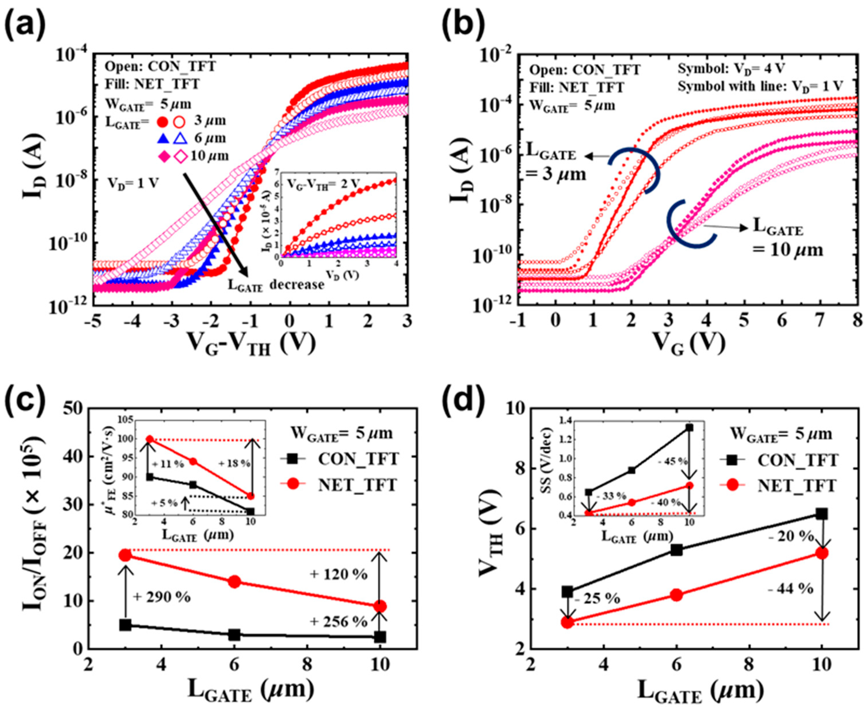
Figure 1. Schematic diagram of fabrication steps of nanonet-channel thin-film transistors (TFTs) using the nanosphere-assisted patterning (NAP) technique.
Micromachines 12 00741 g001
Figure 2. Size of the polystyrene nanosphere as a function of O2 plasma exposure time.
Micromachines 12 00741 g002
Figure 3. Top SEM images of (a) spin coated nanosphere after Figure 1c and (b) nanonet-channel after Figure 1g.
Micromachines 12 00741 g003
Figure 4. Top-view scheme of conventional planar TFTs (CON_TFTs) (left) and nanonet-channel low-temperature polysilicon TFTs (NET_TFTs) (right).
Micromachines 12 00741 g004
Figure 5. Comparison of the DC characteristics for NET_TFTs and CON_TFTs with different LGATE: (a) representative transfer curves (ID vs. VG-VTH), (b) representative transfer curves with VD = 1 and 4 V, (c) an average ON/OFF current ratio, and (d) an average VTH. Insets show the measured output curves (ID vs. VD), μ*FE, and SS as a function of LGATE.
Micromachines 12 00741 g005
Figure 6. Measured ΔVTH and ΔSS (inset) for NET_TFT and CON_TFT with LGATE = 3 μm under an HCI stress condition at VG − VTH = VD = 4 V during 0–1000 s.
Micromachines 12 00741 g006
Figure 7. Cumulative distribution of (a) VTH and (b) SS for NET_TFT and CON_TFT (20 devices).
Micromachines 12 00741 g007
Figure 8. Standard deviation of VTH (σVTH) as a function of LW1/2 for both CON and NET_TFTs.
Micromachines 12 00741 g008
Table 1. Average and standard deviation of VTH and SS for NET_TFTs and CON_TFTs with different LGATE.
Channel
Structure
LGATE
[μm]
AVG. VTH
[V]
STD VTH
[V]
AVG. SS
[V/dec]
STD SS
[V/dec]
conventional33.90.430.650.20
65.30.300.880.16
106.50.231.330.15
nanonet32.90.290.430.09
63.80.200.540.08
105.20.150.720.07
Publisher’s Note: MDPI stays neutral with regard to jurisdictional claims in published maps and institutional affiliations.

