Article

Investigation of a 4H-SiC Trench MOSFET with Back-Side Super Junction

1
College of Electronic and Information Engineering, Shenyang Aerospace University, Shenyang 110136, China
2
School of Integrated Circuits, Tsinghua University, Beijing 100084, China
*
Author to whom correspondence should be addressed.
Micromachines 2022, 13(10), 1770; https://doi.org/10.3390/mi13101770
Submission received: 28 September 2022 / Revised: 13 October 2022 / Accepted: 17 October 2022 / Published: 18 October 2022
(This article belongs to the Special Issue Semiconductor Power Devices: Reliability and Applications)

Abstract

:
In this paper, a 4H-SiC trench gate MOSFET, featuring a super junction layer located on the drain-region side, is presented to enhance the breakdown voltage and the figures of merit (FOM). The proposed structure is investigated and compared with the conventional structure with a 2D numerical simulator—ATLAS. The investigation results have demonstrated that the breakdown voltage in the proposed structure is enhanced by 21.2%, and the FOM is improved by 39.6%. In addition, the proposed structure has an increased short-circuit capability.

1. Introduction

Since the silicon carbide trench-gate metal oxide semiconductor field effect transistor (UMOSFET) was first reported in 1994 [1], researchers have paid significant attention to it due to the excellent material properties of SiC, including a higher critical electric field, a wider band gap and a higher electron saturation drift velocity, compared to silicon [2,3]. However, this reported structure has a serious problem because it cannot reflect the advantage of the silicon carbide material in the withstand voltage, owing to a high electric field existing in the corner of the trench gate oxide [4,5]. In order to overcome this problem, B. J. Baliga proposed a novel UMOSFET incorporated with a P+ shielding region at the bottom of the trench gate [6], which is used to protect the gate oxide from a high electric field. However, at the same time, this also increases the specific on-resistance and power loss of the device by introducing a parasitic JFET region, composed of the p-body, n-drift and P+ shielding region.
Since then, more research has been done on how to reduce the specific on-resistance and increase the breakdown voltage of the UMOSFET devices. The research findings show that there exists a tradeoff between the specific on-resistance and breakdown voltage. Particularly, the figures of merit (FOM) is utilized to indicate the compromise between the two performances, which is defined as FOM = BV2/Ron,sp. Moreover, based on the existing literature, there are two domination ways used to improve the device’s performances. One is to adopt a new structure [7,8,9,10,11,12,13,14,15,16,17,18], with a mechanism that reduces the JFET resistance. The other is adopting a new fabrication process for the gate oxide [19,20,21,22,23,24,25], which increases the channel’s electron mobility to achieve a reduction in the resistance. In this paper, a new trench gate MOSFET is investigated to improve the electrical characteristics of the device.
A 4H-SiC trench gate MOSFET with a back-side super junction layer (called as BSJ-UMOS) is investigated. Compared with a conventional trench gate, MOSFET (C-UMOS), the BSJ-UMOS has a p-type region on the drain-region side, forming a floating super junction, which modulates the electric field in the N-drift region and introduces an exact peak electric field at the p-pillar/n+ substrate region junction. A comparative study between BSJ-UMOS and C-UMOS is conducted in this paper based on a 2D numerical simulator—ATLAS [26]. This paper is organized as follows. The parameters related to the device structure and simulation condition are presented in Section 2. Section 3 presents an analysis and discussion on the simulation results. Finally, we draw a conclusion in Section 4.
Note that due to the limitation of our present experimental conditions, we are unable to provide experimental results, and the simulation tools are generally used for the optimization and development of various semiconductor device structures, in order to reduce the cost of the device manufacturability and development period and, hence, lower the risk of technology transfer in an industrial environment. Moreover, simulation tools are very useful to explore the novel device architectural concept for systems with different materials. So, the aim of the simulation work is to compare the electrical characteristics of two different structures on the same terms, while not revealing the physical devices’ features.

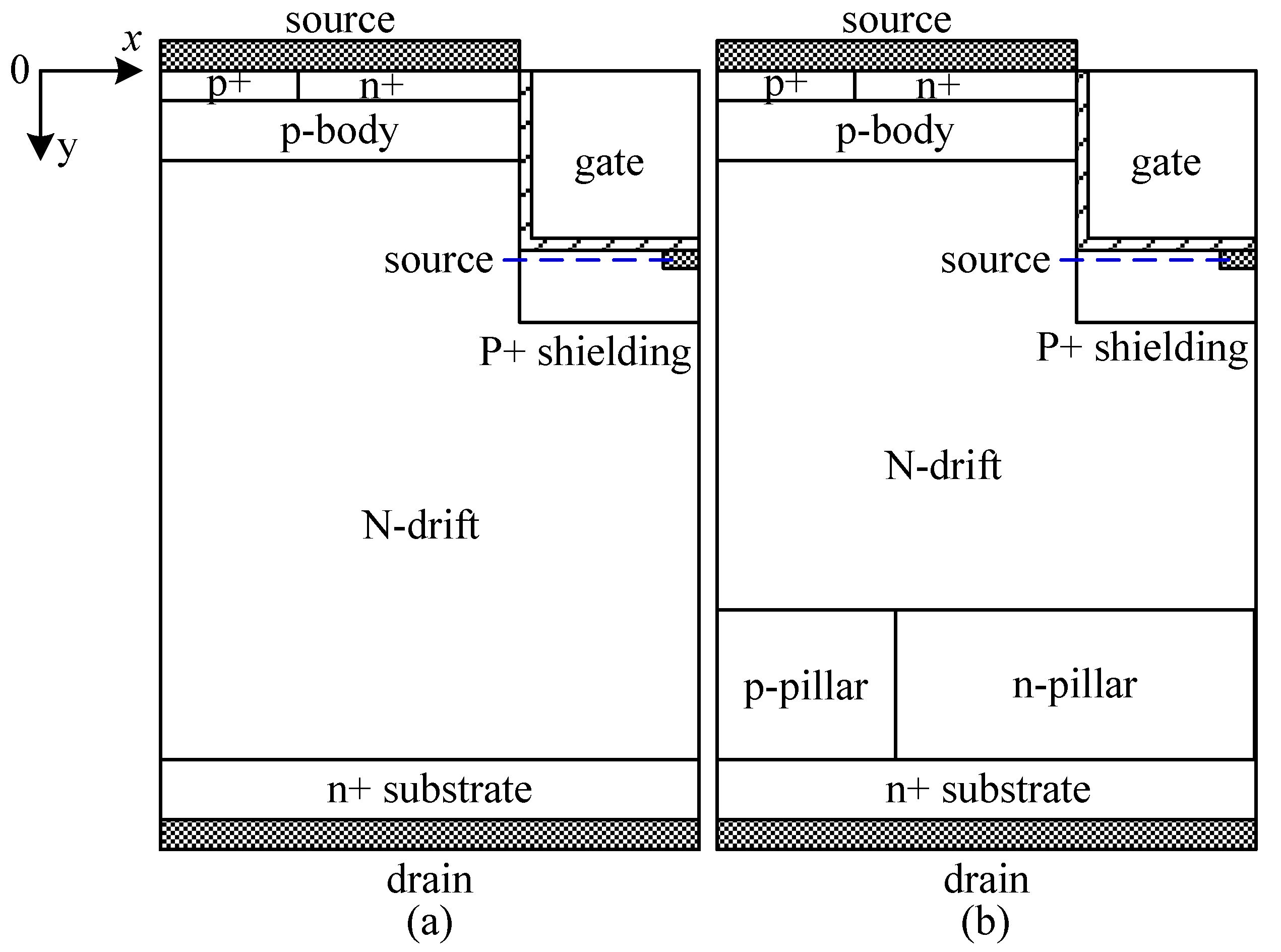
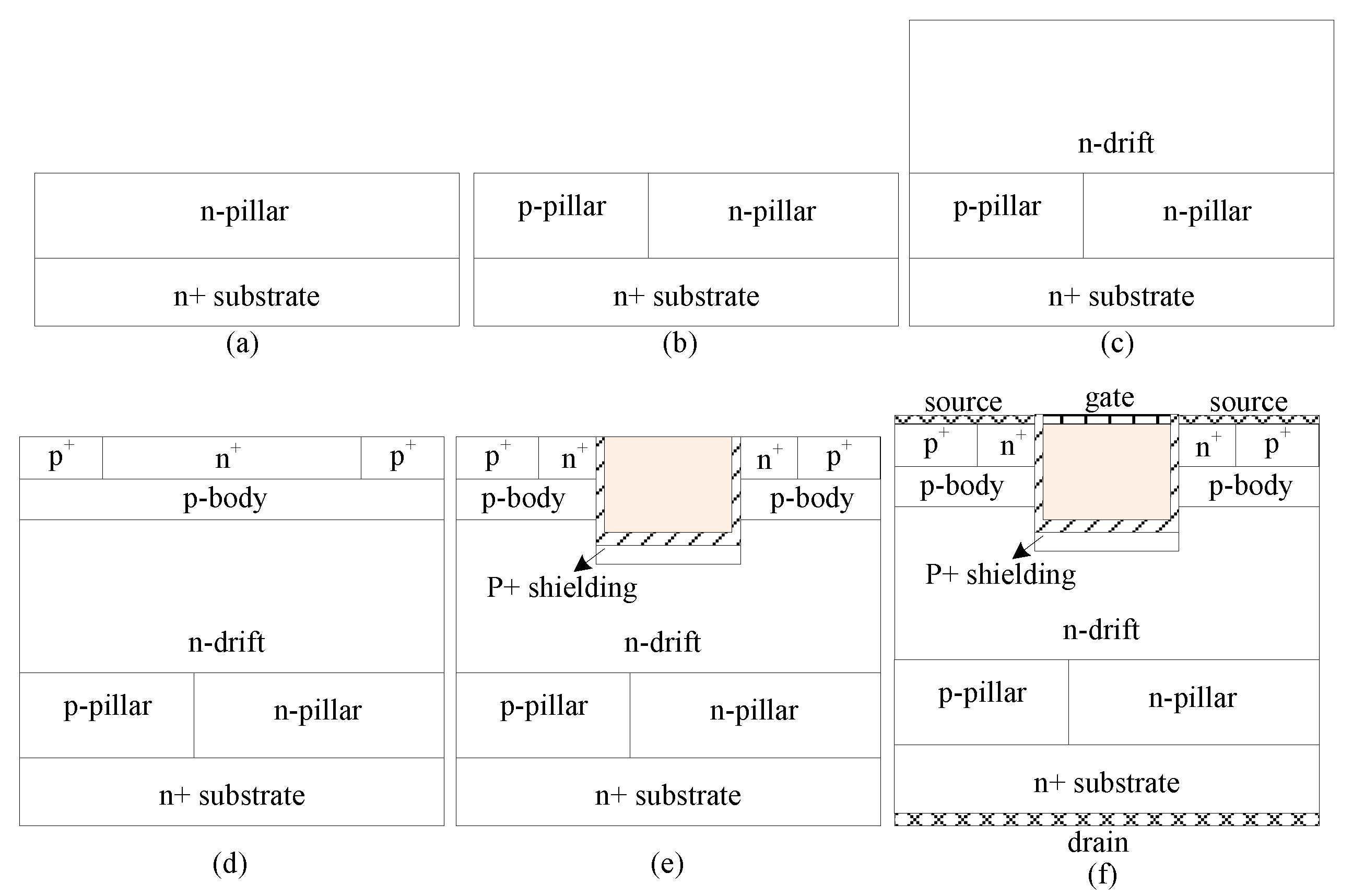
2. Device Structure and Simulation Setup

The 4H-SiC UMOS with a back-side super junction layer (BSJ-UMOS) is as shown in Figure 1b. The drift region of BSJ-UMOS consists of two parts, which are an N-drift region and a super junction layer, composed of the p-pillar and n-pillar. The super junction layer forms extra PN junctions on the drain-region side. As a result, a new electric field peak comes into being, which can modulate the original electric field distribution and improve the breakdown voltage.
Figure 1a shows a cross-sectional schematic of the conventional UMOS (C-UMOS). Note that all the simulation parameters of the two structures are identical, except that there is an extra PN junction at the back side of the proposed structure. The gate oxide thickness is 50 nm. The other simulation parameters are presented in Table 1.
A possible fabrication process for BSJ-UMOS is shown in Figure 2. The key fabrication steps are as follows: (a) forming the n-pillar layer on the n+ wafer by epitaxial growth technology; (b) forming the p-pillar layer by ion implantation; (c) growing the n-drift layer by epitaxial growth technology; (d) forming the p-body layer by epitaxial growth technology and growing the P+ contact region and n+ source region by ion implantation; (e) forming the trench gate structure with the mature silicon carbide fabrication process; (f) metalizing all contacts and forming the gate, source, and drain electrodes. Compared with C-UMOS, such fabrication of BSJ-UMOS would be more complex, as it requires two extra process steps—growing the epitaxial n-pillar layer on the n+ substrate and forming the p-pillar layer via ion implantation.
In this paper, the electrical characteristics of the proposed device are investigated in detail, with a 2D numerical simulator—ATLAS. Since the simulated n-channel IGBT is calibrated with an experimental IGBT [26] device in [27], and these physical models have earlier been applied for 4H-SiC devices [28,29], the simulation is conducted with the same physical models and parameters as [27]. During the simulation, the following models are considered: a bandgap narrowing model (BGN), AUGER and Shockley-Read-Hall (SRH) for recombination and carrier lifetime models and doping- and temperature-dependent field mobility models (ANALYTIC) [30]. Moreover, all simulations are carried out using Fermi Dirac statistics, and Selberherr’s impact ionization model is also utilized [30]. During the simulation, the carrier lifetime in the drift region is set to 1μs, and the channel inversion mobility is 30 cm2/V·s.

3. Analysis and Discussion of Simulation Results

In this section, a comparative investigation between BSJ-UMOS and C-UMOS is carried out for the on-state, off-state and short-circuit performances. The effect of the p-pillar’s parameters on the electrical characteristics is presented in depth.

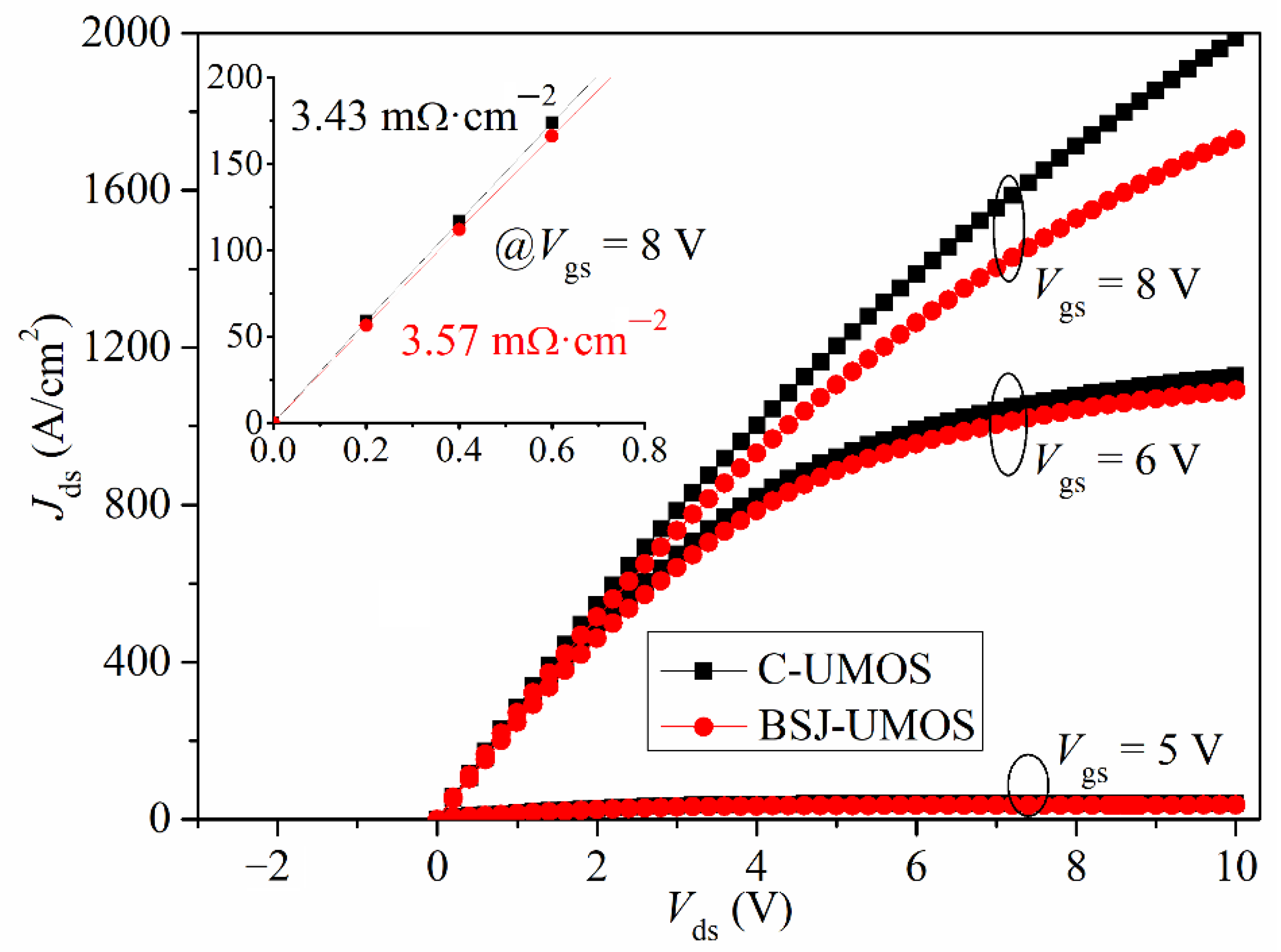
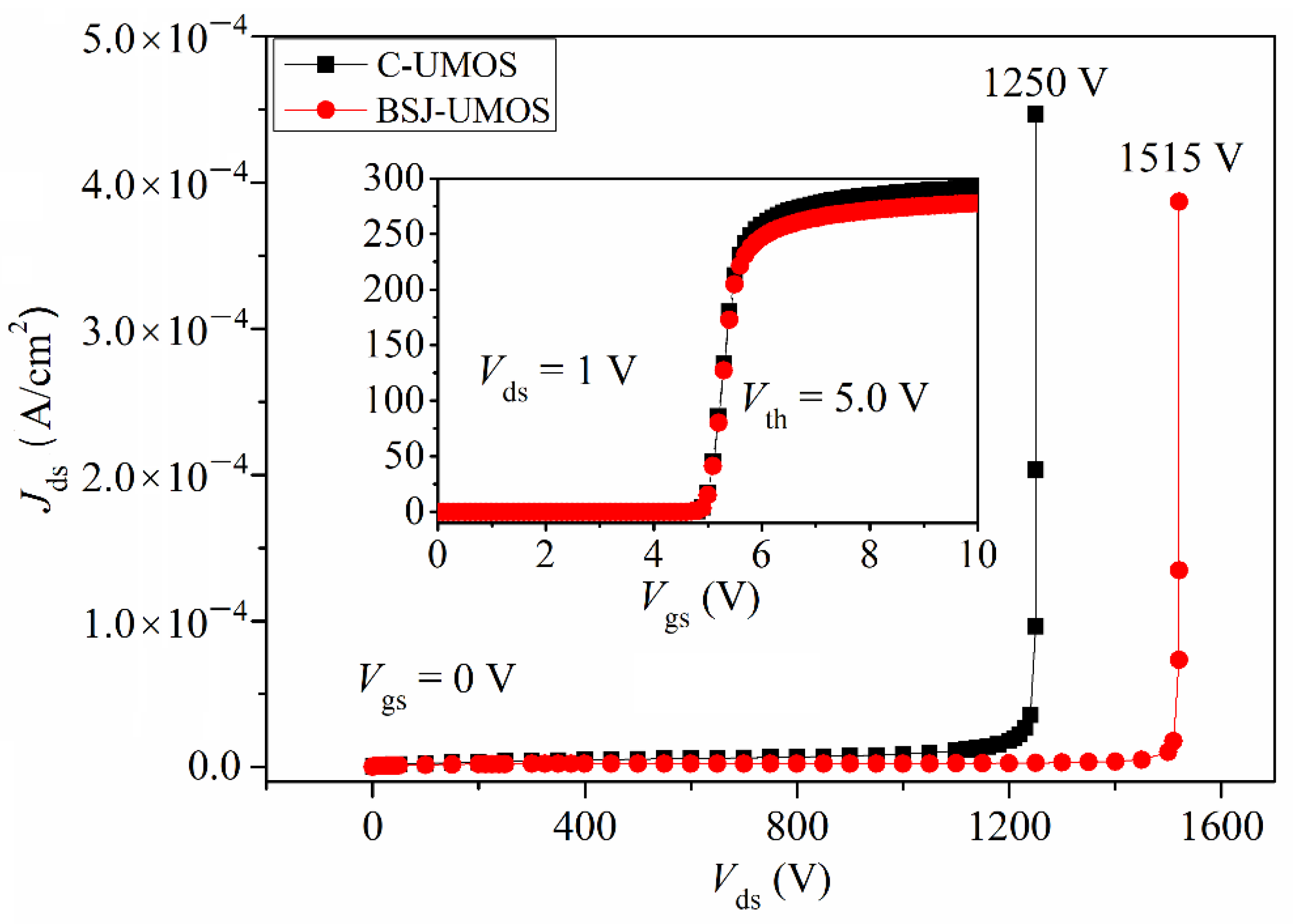
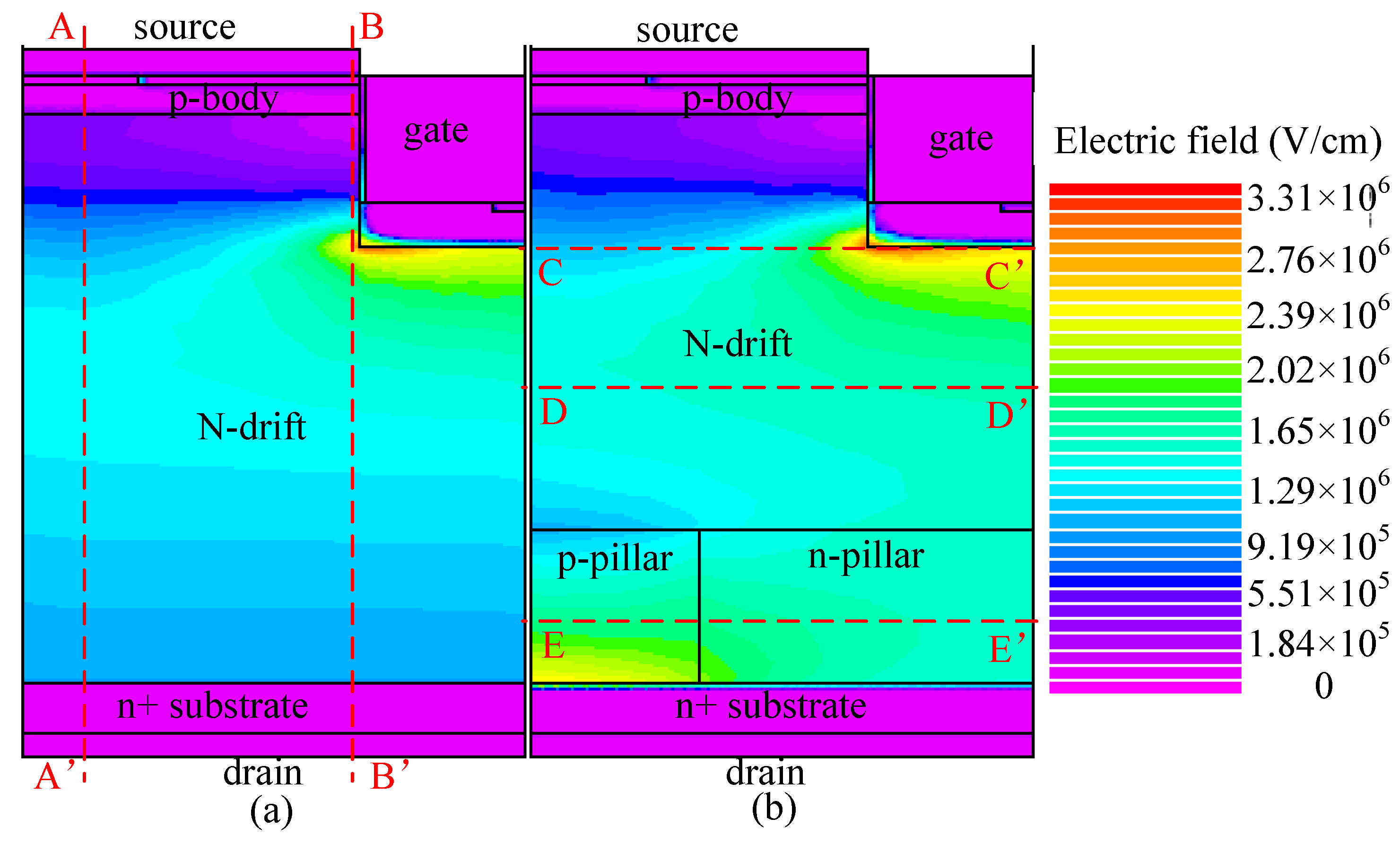
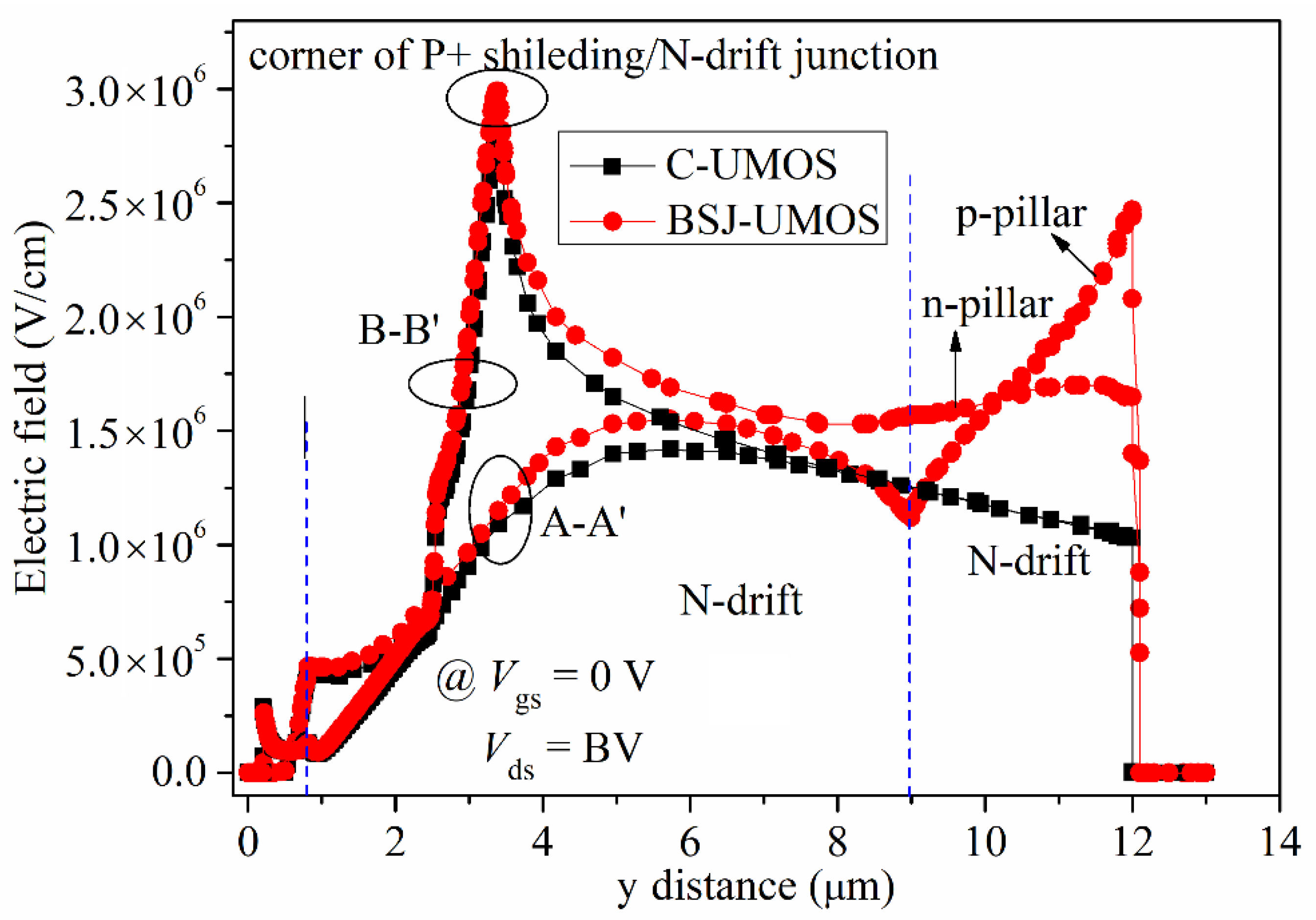
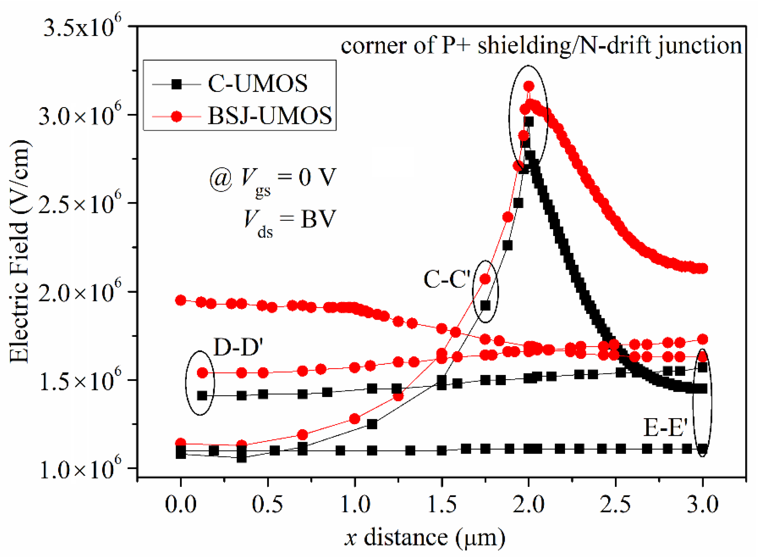
3.1. On and Off Characteristics

The comparison of the I-V characteristic between BSJ-UMOS and C-UMOS is shown in Figure 3. The I-V curves at Vgs = 8 V at the low drain voltage are also given in the inset of Figure 3. From this graph, it can be seen that the forward conduction performance of BSJ-UMOS is slightly degraded. At Jds = 100 A/cm2 and Vgs = 8 V, the specific on-resistance Ron,sp is 3.57 mΩ·cm2 for BSJ-UMOS and increases about 4.08% compared with that for C-UMOS (3.43 mΩ·cm2). The main factor responsible for this is that the existence of the p-pillar region forms a depletion layer in the n-pillar region and narrows down the current flow path. The distribution of the current flowlines in the two structures is shown in Figure 4. The bold red lines represent the depletion layer border, indicating that the current flow path close to the drain region is reduced in BSJ-UMOS.
The transfer characteristic at Vds = 1.0 V for BSJ-UMOS and C-UMOS is presented in the inset of Figure 5. Obviously, the two structures have the same threshold voltage, about 5.0 V. Moreover, it can be seen that BSJ-UMOS has a weak current drive capability because of the introduction of the p-pillar region, which narrows down the current flow path.
The breakdown characteristic is shown in Figure 5. The breakdown voltage is 1515 and 1250 V for BSJ-UMOS and C-UMOS, respectively. The breakdown voltage of BSJ-UMOS is enhanced by 21.2%. This is due to the introduction of the p-pillar/n-pillar junction, which modulates the electric field in the drift region. Figure 6 describes the electric field distribution in BSJ-UMOS and C-UMOS at Vgs = 0 V and Vds = BV. The back-side super junction, composed of the p-pillar and n-pillar region, has two effects on the electric field. One is that the electric field in the drift region of BSJ-UMOS is more well-distributed than in C-UMOS. The other is that there is an additional peak electric field at the p-pillar/n+ substrate junction. These two factors result in the enhancement of the breakdown voltage.
Figure 7 shows a comparison of the electric field distribution of BSJ-UMOS and C-UMOS in the vertical cross-section. From this graph, it can be seen that C-UMOS has only a peak electric field at the P+ shielding/N-drift region junction, and the electric field reduces from the source to the drain side. By contrast, BSJ-UMOS has a two peak electric field. One is almost the same as that of C-UMOS, and the other is at the p-pillar/n+ substrate junction. Moreover, due to the introduction of the p-pillar/n-pillar junction, the electric field intensity from the P+ shielding to the n+ substrate region is well-distributed in BSJ-UMOS. In addition, these lead to an improved breakdown characteristic.
The electric field distribution of BSJ-UMOS and C-UMOS in the lateral cross-section is shown in Figure 8. Due to the existence of the back-side super junction layer, the electric field in the lateral cross-section is significantly strengthened, especially in the p-pillar and n-pillar region, in which the electric field intensity is about double, effectively improving the breakdown voltage of the device.
Next, the performance of BSJ-UMOS and C-UMOS in terms of the FOM values is compared, which indicates the tradeoff between the off-state characteristic (BV) and on-state characteristic (Ron,sp). The FOM values are 652.24 and 467.12 MW/cm2 for BSJ-UMOS and C-UMOS, respectively. In addition, the FOM of BSJ-UMOS is improved by 39.6%, which indicates the significant influence of the back-side super junction layer on the devices’ performances.

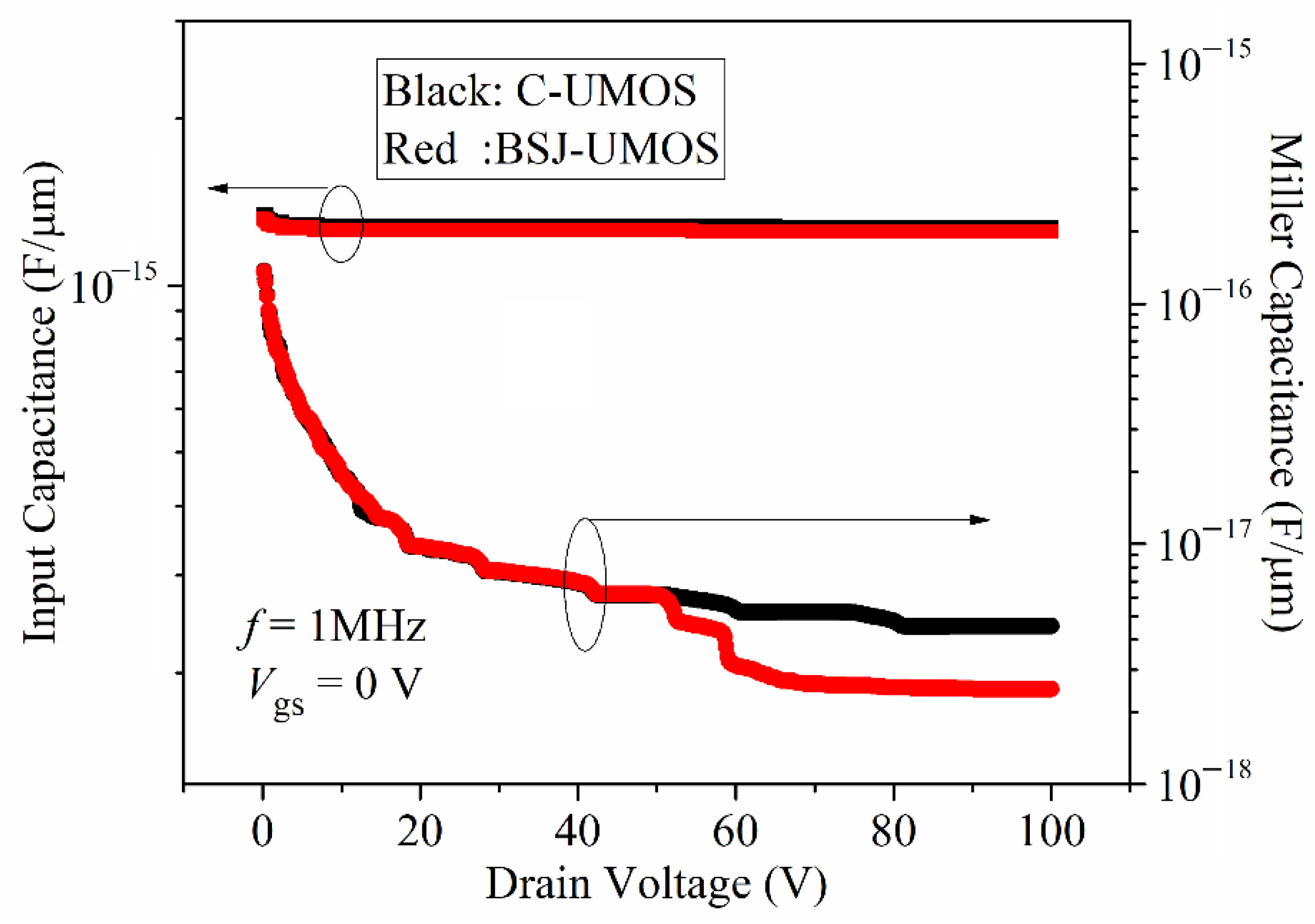
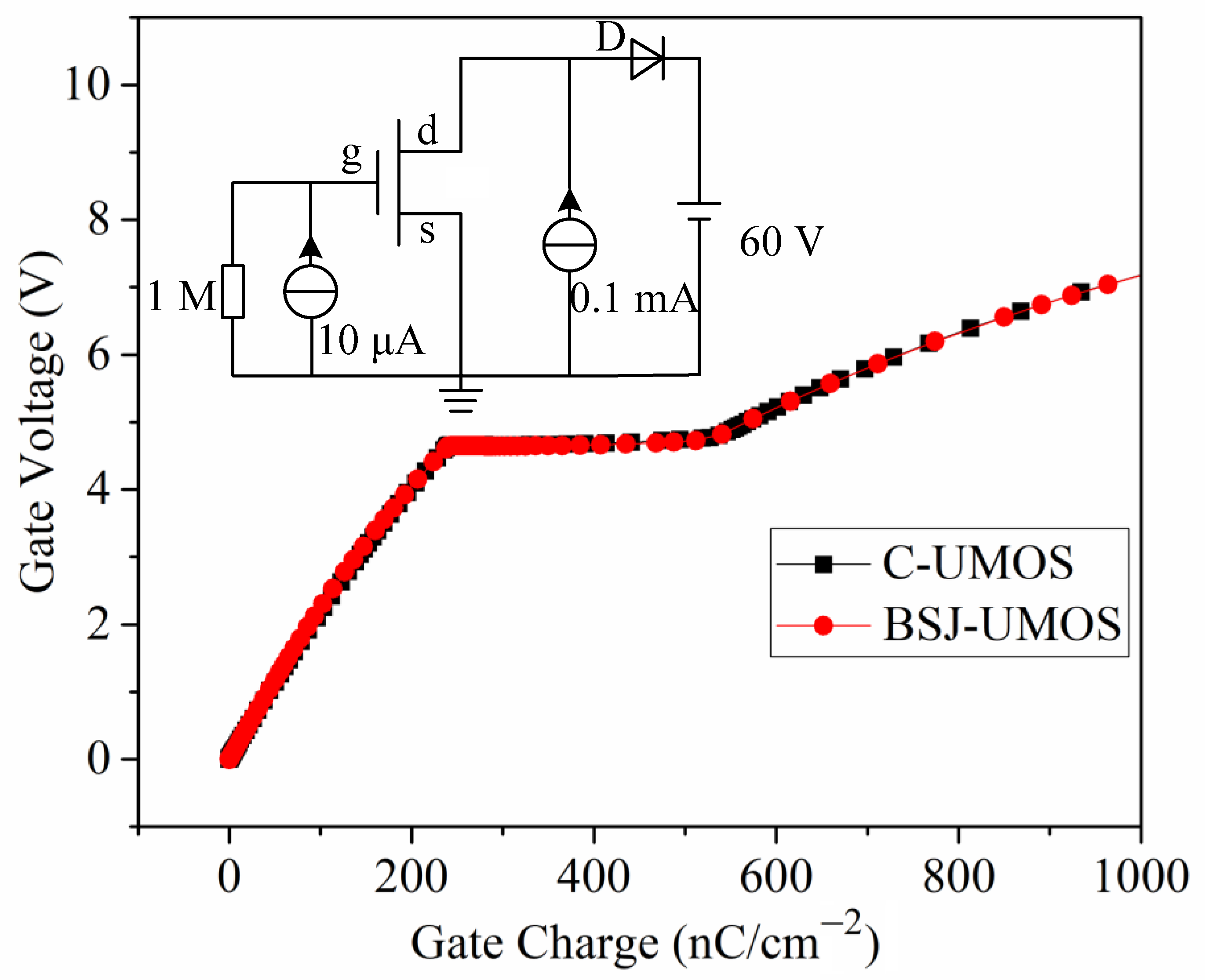
3.2. Other Performances

In this section, the other performances, gate charge and capacitance, are investigated.
Figure 9 plots the parasitic capacitance performance (input capacitance Cies and miller capacitance Cres), indicating that the two structures have almost identical parasitic capacitance when the drain voltage is lower than 60 V. However, when the drain voltage is larger, the BSJ-UMOS has lower miller capacitance, mainly due to the p-pillar making the depletion wider in the n-drift region, as shown in Figure 10. In addition, this is due to the p-pillar being accelerated the depletion of the n-drift region.
The gate charge characteristics and its test circuit are shown in Figure 11. From this, it can be seen that the two structures have an identical gate charge, because the gate charge is mainly dependent on the front structure, and the two structures have the same front structure and parameters.

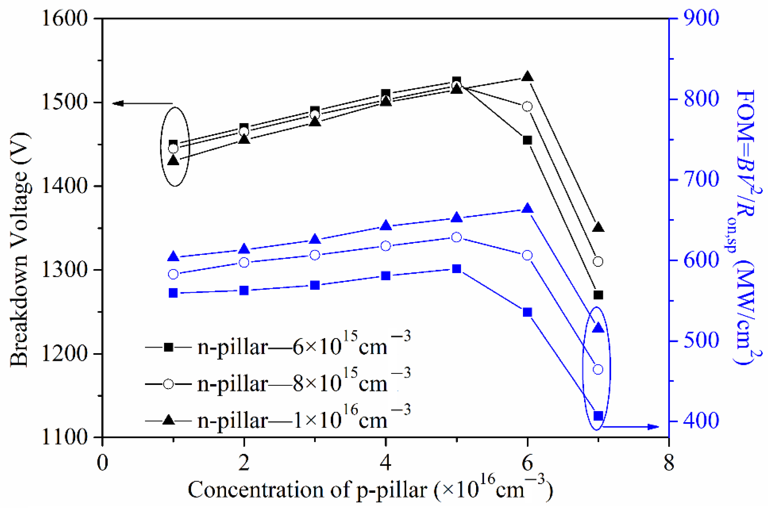
3.3. Parameter Influence

In this section, we investigate the effect of the concentration of the p-pillar and n-pillar on the electrical characteristics, mainly including the breakdown voltage, specific on-resistance and FOM.
Figure 12 shows the effect of the concentration of the p-pillar and n-pillar on the BV and Ron,sp. As we can see from this, with the increasing of the n-pillar’s concentration, the specific on-resistance Ron,sp decreases, and the breakdown voltage is almost unchanged when the p-pillar’s concentration is lower 6 × 1016 cm−3 and then increases. The increasing of the n-pillar’s concentration makes the depletion layer narrower and the current flow path wider, leading to a reduction in Ron,sp. With the increasing of the p-pillar’s concentration, the BV first increases to the maximum value and then decreases, while the Ron,sp is almost unchanged. This is due to the charge in the back-side super junction layer being gradually balanced and then imbalanced, with the increasing of the p-pillar’s concentration. As we can see from Figure 13, the FOM has the same changing trend as the BV, and the changing reason is also the same.

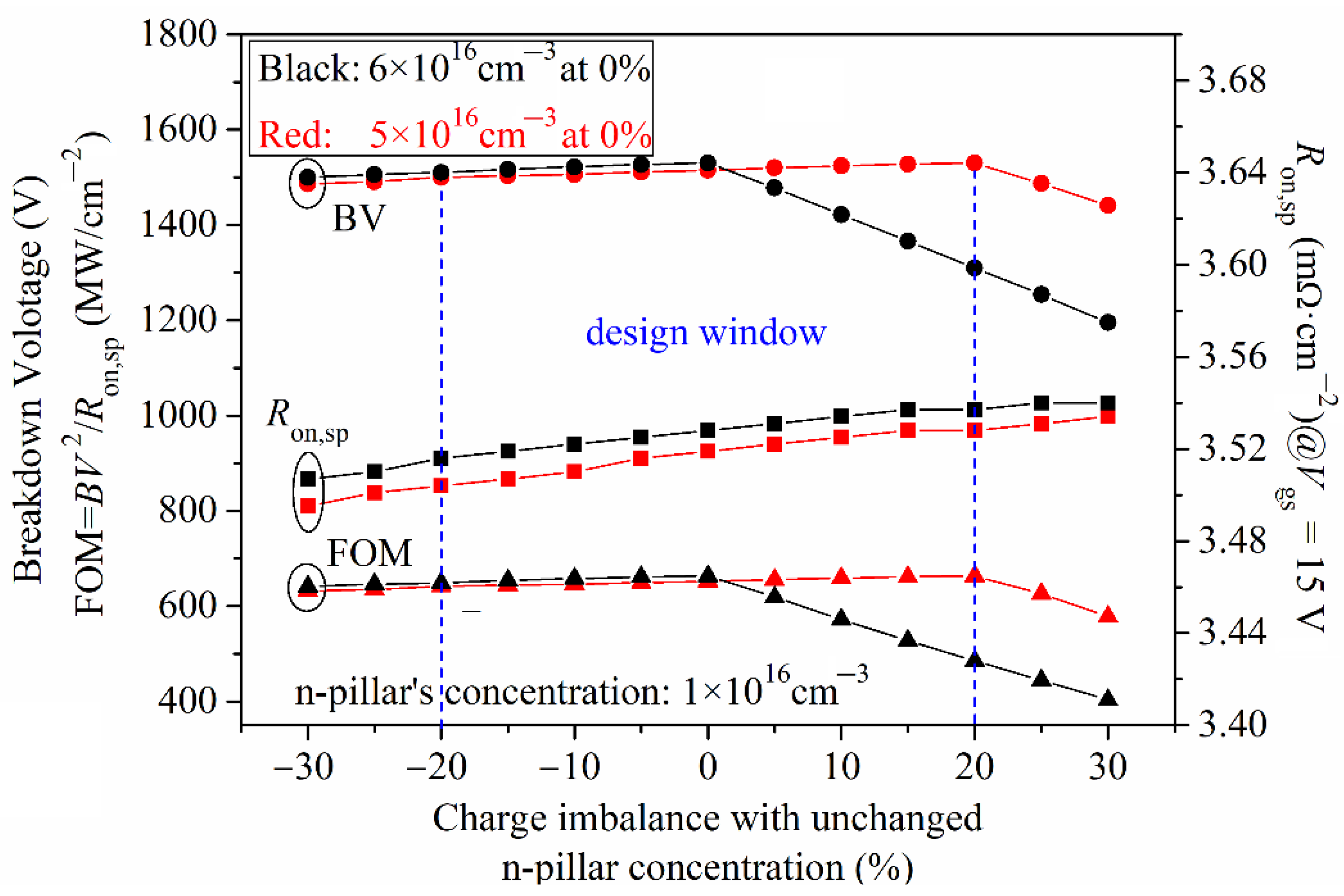
3.4. Charge Imbalance and Design Windows

For a super junction structure, the charge imbalance is unavoidable and is a serious problem that has to be mentioned, especially for silicon carbide device processing technology. Figure 14 shows the relationship curve of the BV, Ron,sp and FOM versus the charge imbalance in BSJ-UMOS. Ideally, the highest BV can be obtained when the charge is balanced. However, when the charge balance is broken, the breakdown voltage begins to decline from the highest value. A charge imbalance, changing from negative to positive, means that the p-pillar’s concentration increases, the depletion layer narrows down and, thus, the Ron,sp increases, as Figure 14 shows. From Figure 13, we can see that the highest BV and FOM are achieved when the concentrations of the p-pillar and n-pillar are 6 × 1016 cm−3 and 1 × 1016 cm−3, respectively. However, from Figure 14, it can be seen that the design window is wider when the concentration of the p-pillar is 5 × 1016 cm−3. In this design window, when the charge imbalance changes from –20% to 20%, the breakdown voltage is about 1500 V, and the FOM ranges from 642.12 to 663.52 MW/cm2, which is easy for the control of the process technology.

3.5. Short-Circuit Capability

The short-circuit case is defined as follows: when the 4H-SiC MOSFET operates in the conduction mode, the high-voltage source is directly biased at the drain electrode, due to the shorting of the load [31,32]. At the same time, a high drain current flows through the device with a high drain voltage, which generates a high power loss and makes the device’s temperature increase. From the I-V performance (shown in Figure 3), the BSJ-UMOS has a lower saturation current due to the introduction of the p-pillar, meaning an increased short-circuit capability. The test circuit of the short-circuit characteristic is shown in Figure 15, and the simulation results are presented in Figure 16, in which the drain current pulse is caused by the inductance load. As expected, compared with C-UMOS, BSJ-UMOS has a lower drain current and minimum lattice temperature during the short-circuit case, since the existence of the p-pillar shrinks the current flow path. Owing to the lower lattice temperature, BSJ-UMOS has an improved short-circuit capability.

4. Conclusions

A 4H-SiC trench gate MOSFET structure with a super junction layer (composed of the p-pillar and n-pillar) on the drain-region side is investigated in detail and compared with a conventional trench gate, MOSFET. The investigation results demonstrate that the proposed structure can significantly enhance the breakdown voltage, with a slight degradation of the specific on-resistance. The introduction of a back-side super junction layer can modulate the electric field in the drift region and introduce an exact peak electric field at the p-pillar/n+ substrate junction, resulting in a significant improvement in the FOM. Moreover, BSJ-UMOS has an increased short-circuit capability due to a lower saturation current.

Author Contributions

Conceptualization, L.Z. and Y.L. (Yanjuan Liu); investigation, L.Z., Y.L. (Yuxuan Liu) and J.F.; methodology, Y.L. (Yuxuan Liu) and Y.L. (Yanjuan Liu); software, L.Z., Y.L. (Yuxuan Liu), J.F. and Y.L. (Yanjuan Liu); validation, Y.L. (Yuxuan Liu), J.F. and Y.L. (Yanjuan Liu); writing—original draft, L.Z.; writing—review and editing, L.Z., Y.L. (Yuxuan Liu), J.F. and Y.L. (Yanjuan Liu) All authors have read and agreed to the published version of the manuscript.

Funding

This research was funded by a project of the Liaoning Provincial Department of Education, grant number LJKZ0174; the Natural Science Foundation of Liaoning Province, grant number 2021-BS-192; and by the Ph.D. research startup foundation of Shenyang Aerospace University, grant number 19YB47.

Institutional Review Board Statement

Not applicable.

Informed Consent Statement

Not applicable.

Data Availability Statement

Not applicable.

Conflicts of Interest

The authors declare no conflict of interest.

References

  1. Palmour, J.W.; Edmond, J.A.; Kong, H.; Charter, C. Vertical Power Devices in Silicon Carbide. In Silicon Carbide and Related Materials; Trans Tech Publications Ltd.: Zurich, Switzerland, 1994; pp. 499–502. [Google Scholar]
  2. Cooper, J.; Melloch, M.; Singh, R.; Agarwal, A.; Palmour, J. Status and Prospects for SiC Power MOSFETs. IEEE Trans. Electron. Devices 2004, 49, 658–664. [Google Scholar] [CrossRef]
  3. Östling, M.; Ghandi, R.; Zetterling, C. SiC Power Devices–Present Status, Applications and Future Perspective. In Proceedings of the 2011 IEEE 23rd International Symposium on Power Semiconductor Devices and ICs, San Diego, CA, USA, 23–26 May 2011; pp. 10–15. [Google Scholar]
  4. Friedrichs, P.; Burte, E.P.; Schorner, R. Dielectric Strength of Thermal Oxides on 6H-SiC and 4H-SiC. Appl. Phys. Lett. 1994, 65, 1665–1667. [Google Scholar] [CrossRef]
  5. Shenoy, J.N.; Das, M.K.; Cooper, J.A.; Melloch, M.R.; Palmour, J.W. Effort of Substrate Orientation and Crystal Anisotropy on the Thermally Oxidized SiO2/SiC Interface. J. Appl. Phys. 1996, 79, 3042–3045. [Google Scholar] [CrossRef]
  6. Baliga, B.J. Silicon Carbide Switching Device with Rectifying Gate. U.S. Patent 5 396 085, 7 March 1995. [Google Scholar]
  7. Zhang, Q.; Gomez, M.; Bui, C.; Hanna, E. 1600 V 4H-SiC UMOSFETs with Dual Buffer Layers. In Proceedings of the International Symposium on Power Semiconductor Devices and ICs, Santa Barbara, CA, USA, 23–26 May 2005; pp. 211–214. [Google Scholar]
  8. Nakano, Y.; Nakamura, R.; Sakairi, H.; Mitani, S.; Nakamura, T. 690 V, 1.00 mΩ·cm2 4H-SiC Double-Trench MOSFETs. Mater. Sci. Forum 2012, 717–720, 1069–1072. [Google Scholar] [CrossRef]
  9. Orouji, A.A.; Jozi, M.; Fathipour, M. High-Voltage and Low Specific On-Resistance Power UMOSFET Using P and N Type Columns. Mater. Sci. Semicond. Process. 2015, 39, 711–720. [Google Scholar] [CrossRef]
  10. Saitoh, Y.; Hiyoshi, T.; Wada, K.; Masuda, T.; Tsuno, T. 4H-SiC V-Groove Trench MOSFETs with The Buried P+ Regions. Sei Tech. Rev. 2015, 80, 75–80. [Google Scholar]
  11. Peyvast, N.; Fathipour, M. A Novel 4H-SiC UMOSFET_ACCUFET with Large Blocking Voltage. In Proceedings of the 1st International Symposium on Quality Electronic Design, Barcelona, Spain, 14–18 June 2009; pp. 35–38. [Google Scholar]
  12. Wang, Y.; Tian, K.; Hao, Y.; Yu, C.H.; Liu, Y.J. 4H–SiC Step Trench Gate Power Metal–Oxide–Semiconductor Field-Effect Transistor. IEEE Electron. Device Lett. 2016, 37, 633–635. [Google Scholar] [CrossRef]
  13. Song, Q.; Yang, S.; Tang, G.N.; Han, C.; Zhang, Y.; Tang, X.; Zhang, Y. 4H-SiC Trench MOSFETs with L Shaped Gate. IEEE Electron. Device Lett. 2016, 37, 463–466. [Google Scholar] [CrossRef]
  14. Wei, J.; Zhang, M.; Jiang, H.; Cheng, C.-H.; Chen, K.J. Low ON-Resistance SiC Trench/Planar MOSFET With Reduced OFF-State Oxide Field and Low Gate Charges. IEEE Electron. Device Lett. 2016, 37, 1458–1461. [Google Scholar] [CrossRef]
  15. Zhang, M.; Wei, J.; Jiang, H.; Chen, K.J.; Cheng, C.H. A New SiC Trench MOSFET Structure With Protruded p-Base for Low Oxide Field and Enhanced Switching Performance. IEEE Trans. Device Mater. Reliab. 2017, 17, 432–437. [Google Scholar] [CrossRef]
  16. Zhou, X.T.; Yue, R.F.; Zhang, J.; Dai, G.; Li, J.; Wang, Y. 4H-SiC Trench MOSFET With Floating/Grounded Junction Barrier-controlled Gate Structure. IEEE Trans. Electron. Devices 2017, 64, 4568–4574. [Google Scholar] [CrossRef]
  17. Bharti, D.; Islam, A. Optimization of SiC UMOSFET Structure for Improvement of Breakdown Voltage and ON-Resistance. IEEE Trans. Electron. Devices 2018, 65, 615–621. [Google Scholar] [CrossRef]
  18. Yang, T.T.; Wang, Y.; Yue, R.F. SiC Trench MOSFET with Reduced Switching Loss and Increased Short-circuit Capability. IEEE Trans. Electron. Devices 2020, 67, 3685–3690. [Google Scholar] [CrossRef]
  19. Chung, G.Y.; Tin, C.C.; Williams, J.R.; McDonald, K.; Chanana, R.K.; Weller, R.A.; Palmour, J.W. Improved Inversion Channel Mobility for 4H-SiC MOSFETs Following High Temperature Anneals in Nitric Oxide. IEEE Electron. Device Lett. 2001, 22, 176–178. [Google Scholar] [CrossRef]
  20. Constant, A.; Camara, N.; Montserrat, J.; Pausas, E.; Camassel, J.; Godignon, P. Oxidation Process by RTP for 4H-SiC MOSFET Gate Fabrication. Mater. Sci. Forum 2011, 679–680, 500–503. [Google Scholar] [CrossRef]
  21. Chanthaphan, A.; Hosoi, T.; Shimura, T.; Watanabe, H. Study of SiO2/4H-SiC Interface Nitridation by Post-Oxidation Annealing in Pure Nitrogen Gas. Aip Adv. 2015, 111, 097134. [Google Scholar] [CrossRef]
  22. Dai, O.; Yano, H.; Hirata, K.; Hatayama, T.; Fuyuki, T. Improved Inversion Channel Mobility in 4H-SiC MOSFETs on Si Face Utilizing Phosphorus-Doped Gate Oxide. IEEE Electron. Device Lett. 2010, 31, 710–712. [Google Scholar]
  23. Sledziewski, T.; Weber, H.B.; Krieger, M. Passivation and Generation of States at P-Implanted Thermally Grown and Deposited N-Type 4H-SiC/SiO2 Interfaces. Mater. Sci. Forum 2016, 858, 697–700. [Google Scholar] [CrossRef]
  24. Dai, O.; Sometani, M.; Harada, S.; Kosugi, R.; Yonezawa, Y.; Yano, H. Improved Channel Mobility in 4H-SiC MOSFETs by Boron Passivation. IEEE Electron. Device Lett. 2014, 35, 1176–1178. [Google Scholar]
  25. Cabello, M.; Soler, V.; Montserrat, J.; Rebollo, J.; Rafí, J.M.; Godignon, P. Impact of Boron Diffusion on Oxynitrided Gate Oxides in 4H-SiC Metal-Oxide-Semiconductor Field-Effect Transistors. Appl. Phys. Lett. 2017, 111, 321–337. [Google Scholar] [CrossRef]
  26. Ryu, S.H.; Capell, C.; Cheng, L.; Jonas, C.; Gupta, A.; Donofrio, M.; Bhattacharya, S. High performance, ultra high voltage 4H-SiC IGBTs. In 2012 IEEE Energy Conversion Congress and Exposition (ECCE); IEEE: Raleigh, North Carolina, 2012; pp. 3603–3608. [Google Scholar]
  27. Usman, M.; Nawaz, M. Device design assessment of 4H–SiC n-IGBT—A simulation study. Solid-State Electron. 2014, 92, 5–11. [Google Scholar] [CrossRef]
  28. Muhammad, N.; Chimento, F. On the assessment of temperature dependence of 10–20 kV 4H-SiC IGBTs using TCAD. Mater. Sci. Forum 2013, 740–742, 1085–1088. [Google Scholar]
  29. Buono, B.; Ghandi, R.; Domeij, M.; Malm, B.G.; Zetterling, C.M.; Ostling, M. Modeling and characterization of current gain versus temperature in 4H-SiC power BJTs. IEEE Trans. Electron. Devices 2010, 57, 704–711. [Google Scholar] [CrossRef]
  30. Silvaco Int. Two-Dimensional Device Simulation Program; Silvaco Int.: Santa Clara, CA, USA, 2012. [Google Scholar]
  31. Namai, M.; An, J.; Yano, H.; Iwamuro, N. Experimental and Numerical Demonstration and Optimized Methods for SiC Trench MOSFET Short-Circuit Capability. In Proceedings of the 2017 29th International Symposium on Power Semiconductor Devices and IC’s (ISPSD), Sapporo, Japan, 28 May–1 June 2017; Volume 3, pp. 7–10. [Google Scholar]
  32. Tanaka, R.; Kagawa, Y.; Fujiwara, N.; Sugawara, K.; Fukui, Y.; Miura, N.; Yamakawa, S. Impact of Grounding the Bottom Oxide Protection Layer on The Short-Circuit Ruggedness of 4H-SiC Trench MOSFETs. In Proceedings of the 2014 IEEE 26th International Symposium on Power Semiconductor Devices & IC’s (ISPSD), Waikoloa, HI, USA, 15–19 June 2014; pp. 75–78. [Google Scholar]
Figure 1. Cross-sectional schematic of a half-cell in (a) C-UMOS and (b) BSJ-UMOS.
Micromachines 13 01770 g001
Figure 2. A possible fabrication process for BSJ-UMOS (a) growth of the n-pillar layer on n+ substrate (b) growth of the p-pillar layer by ion implantation (c) growth of the n-drift layer (d) growth of the p-body, n+ source and p+ contact regions (e) forming the trench gate structure (f). metalizing all contacts.
Micromachines 13 01770 g002
Figure 3. Comparison of I-V characteristic curves.
Micromachines 13 01770 g003
Figure 4. Distributions of current flowlines at Jds = 100 A/cm2 in (a) C-UMOS and (b) BSJ-UMOS.
Micromachines 13 01770 g004
Figure 5. Comparisons of transfer and breakdown characteristics.
Micromachines 13 01770 g005
Figure 6. Electric field distributions at Vgs = 0 V and Vds = BV in (a) C-UMOS and (b) BSJ-UMOS.
Micromachines 13 01770 g006
Figure 7. Electric field distributions of the BSJ-UMOS and C-UMOS along the AA’ (x = 0.5 μm) and BB’ (x = 2.0 μm) lines, as shown in Figure 5a.
Micromachines 13 01770 g007
Figure 8. Electric field distributions of BSJ-UMOS and C-UMOS along CC’ (y = 3.4 μm), DD’ (y = 6.0 μm) and EE’ (y = 11 μm) lines, as shown in Figure 5b.
Micromachines 13 01770 g008
Figure 9. Comparisons of the parasitic capacitance in C-UMOS and BSJ-UMOS.
Micromachines 13 01770 g009
Figure 10. Depletion distributions of (a) C-UMOS and (b) BSJ-UMOS at Vds = 70 V and Vgs = 0 V.
Micromachines 13 01770 g010
Figure 11. Comparisons of the gate charge performances.
Micromachines 13 01770 g011
Figure 12. Effect of concentration of the p-pillar and n-pillar on the BV and Ron,sp.
Micromachines 13 01770 g012
Figure 13. Effect of the concentration of the p-pillar and n-pillar on the BV and FOM.
Micromachines 13 01770 g013
Figure 14. Relationship curves of BV, Ron,sp and FOM versus charge imbalance for BSJ-UMOS.
Micromachines 13 01770 g014
Figure 15. Test circuit of the short-circuit performance.
Micromachines 13 01770 g015
Figure 16. Maximum lattice temperature and drain current for the short-circuit case.
Micromachines 13 01770 g016
Table 1. Structural parameters of the simulated devices.
ParametersC-UMOSBSJ-UMOS
Concentration of n+/p+ region (cm−3) 1.0 × 10 19 1.0 × 10 19
Concentration of p-body region (cm−3) 1.0 × 10 17 1.0 × 10 17
Thickness of p-body region (μm) 0.6 0.6
Width of trench gate (μm) 1.0 1.0
Depth of trench gate (μm) 2.5 2.5
Concentration of P+ shielding region (cm−3) 1.0 × 10 18 1.0 × 10 18
Concentration of N-drift region (cm−3) 4.0 × 10 15 4.0 × 10 15
Thickness of N-drift region (μm) 11.2 8.2
Concentration of p-pillar (cm−3) - 5 × 10 16
Thickness of p-pillar region (μm) - 3
Width of p-pillar region (μm) - 1
Concentration of n-pillar region (cm−3) - 1 × 10 16
Thickness of n-pillar region (μm) - 3
Width of n-pillar region (μm) - 2
Concentration of n+ substrate region (cm−3) 1 × 10 19 1 × 10 19
Width of a half cell (μm) 3 3
Publisher’s Note: MDPI stays neutral with regard to jurisdictional claims in published maps and institutional affiliations.

