

Electrical Performance of 28 nm-Node Varying Channel-Width nMOSFETs under DPN Process Treatments

1
Department of Electronic Engineering, Minghsin University of Science and Technology, Hsinchu 30401, Taiwan
2
Department of Electrical Engineering, National University of Kaohsiung, Kaohsiung 81148, Taiwan
3
Department of Reliability Engineering, Chingis Technology Corporation, Hsinchu 30078, Taiwan
*
Authors to whom correspondence should be addressed.
Micromachines 2022, 13(11), 1861; https://doi.org/10.3390/mi13111861
Submission received: 29 August 2022
/
Revised: 20 October 2022
/
Accepted: 27 October 2022
/
Published: 29 October 2022
(This article belongs to the Special Issue III–V Compound Semiconductors and Devices)
Abstract
:The decoupled-plasma nitridation treatment process is an effective recipe for repairing the trap issues when depositing high-k gate dielectric. Because of this effect, electrical performance is not only increased with the relative dielectric constant, but there is also a reduction in gate leakage. In the past, the effect of nitridation treatment on channel-length was revealed, but a channel-width effect with that treatment was not found. Sensing the different nano-node channel-width n-channel MOSFETs, the electrical characteristics of these test devices with nitridation treatments were studied and the relationship among them was analyzed. Based on measurement of the VT, SS, Gm, ION, and IOFF values of the tested devices, the electrical performance of them related to process treatment is improved, including the roll-off effect of channel-width devices. On the whole, the lower thermal budget in nitridation treatment shows better electrical performance for the tested channel-width devices.
1. Introduction
With regard to the complexity increment of nano-node process manufacturing, each process recipe in the production line will greatly impact the yield or the throughput of integrated-circuit (IC) products [1,2]. Even though the hot 3-nm IC mass-production technology at the present stage adopts a fin metal-oxide-semiconductor field-effect transistor (fin MOSFET or FinFET) [3,4,5,6,7], providing the better gate controllability, the high-k gate dielectric [8,9] is still a useful material with which to increase the drive current, ION, related to the high-speed performance of ICs. Below 3-nm node process, the multi-nano-sheet field-effect transistors [10,11,12,13] with gate-all-around modality are more suitable candidates. Using the high-k dielectric is still a good choice for maintaining a higher drive current than that achieved with silicon dioxide or silicon nitride [14].
Because the high-k gate dielectric still supports an excellent k-value, more so than silicon dioxide, reducing the disadvantages of the high-k dielectric, such as the numerous traps in the atomic deposition of gate dielectric and the interface between channel surface and gate dielectric, is important. Using the thin interfacial layer is a feasible way of decreasing the interface state density and strengthening the bonding between the gate dielectric and the Si-based channel surface. Moreover, optimal nitridation treatment allows repair of the oxygen vacancy or bulk traps in the gate dielectric. Possible and cost-effective nitridation treatments include post-deposition annealing (PDA) and decoupled-plasma nitridation (DPN) processes [15,16]. According to the published literature [17], the PDA process in is more impressive in terms of cost, but the DPN process seems better in electrical performance due to the larger nitrogen free radicals fixing the traps more effectively. The major variables of DPN treatment processes in plasma systems include the radio-frequency power, nitrogen concentration, and treatment temperatures. Because the complementary MOSFET (CMOSFET), composed of an n-channel MOSFET (nMOSFET) and a p-channel MOSFET (pMOSFET), is the mainstay and foundation stone of logic, it has applications in data communication, data processing, and high-performance computing (HPC) IC products. The nano-node device model [18], a device with short-channel effect performance [19] and reliability [20,21], is more well suited to the development of electronic-design-automation (EDA) software [22]. Because the commercial EDA software is a good tool for IC designers, ultra-large-scale-integration ICs can be precisely designed and completed. However, few reports in the literature mention the nano-node channel-width effect after process variation. In this work, we aim to vary the nitrogen concentration and treatment temperatures impacting the electrical performance of channel-width devices after the deposition of high-k gate dielectric. These efforts will help to establish a set of precise device models with regard to channel-width after process variation.
The paper is organized as follows: In Section 2, an outline of semiconductor processes and a flow chart of electrical measurements are presented. In Section 3, the main sensing electrical results for each tested device and the analysis of nano-node channel-width performance are discussed. Moreover, the lower thermal budget of DPN treatment, on the whole, demonstrates better electrical performance among the three tested process groups. Finally, a summary of the precious findings and conclusions of this work is presented in Section 4.
2. Outline of Semiconductor Processes and Measurement Establishment
Although 28 nm-node processes have been gradually adopted at the mature process level, nitridation treatment in high-k gate dielectric can still be adopted for the novel 3 nm-node manufacturing process with FinFET format. The gate-last process [23,24] in the front-end level is more favored in integration consideration due to avoiding source/drain (S/D) diffusion after high-temperature annealing, impacting the metal gate instead of the poly-silicon electrode. Thus, substituting the traditional front-end process with the gate-last is necessary, and using low-resistance aluminum as the metal gate can improve the gate delay and power consumption. Incorporating the high-k HfO2, ZrO2, or sandwiched HfO2/ZrO2/HfO2 as the gate dielectric is a good way to increase the drive current and reduce the gate leakage, compared with silicon oxide at the equivalent oxide thickness [25]. In conventional planar MOSFET manufacturing, the active area (AA) must be defined first. The well and VT adjustment implants, forming the N- and P-wells and controlling the feasible VT values, are followed continuously. The sacrificial oxide is grown first and then removed. The true gate oxide is thermally grown. Furthermore, the poly-gate electrodes are produced using with chemical vapor deposition (CVD), dry etch technology and suitable photolithography. To reduce the hot-carrier effect, the S/D extension implant is used. The sidewall spacer shape is deposited and etched. After that, S/D implants and high-temperature annealing are used. The pre-metal dielectric, to provide device isolation, is deposited using low-temperature CVD technology. In addition, a contact mask is applied to form the gate contact (CT) and S/D CT. In addition, the first metal (M1) mask, made using with copper damascene [26,27] plus chemical-mechanical polishing, is used to gain the desired metal format. Finally, passivation and pad-window processes are completed to monitor the front-end device performance. For the gate-last processes, the poly-gate is treated as a dummy gate. The interfacial layer, SiOx, is deposited first with rapidly thermal oxidation process, before the 24 Å physical thickness of high-k dielectric deposition using an atomic-layer deposition process. This process is beneficial because it reduces the interface state density between the high-k gate dielectric and the channel surface and indirectly increases channel mobility. Generally, the hafnium dielectric is deposited early on in the flow, before a sacrificial poly-gate is created. After the high-temperature S/D and poly-silicide annealing cycles, the dummy gate is removed and Al-gate electrodes are deposited last. The remaining back-end processes with single damascene copper layer as the first metal layer were followed.
The overall complexity and process costs are slightly escalated, but the increase in electrical performance and decrease in power consumption is impressive. In this work, the tested wafers with gate-last processes were of an engineering type, the back-end metal was completed before the first metal (M1) plus passivation and pad window processes were begun, as shown in Figure 1. The abbreviations, W, L, SDE, and n+, in Figure 1 are channel-width, channel-length, source/drain extension implant [28], and heavily doped S/D implant, respectively. The dog-bone layout [29] has two advantages: eliminating the risk of gate-electrode peeling and avoiding the serious corner rounding in photolithography. After depositing the high-k gate dielectric, the nitridation treatment with the designed nitrogen concentration and annealing temperature was followed. In this work, three kinds of nitridation process splits are itemized as DPN-I, II, and III, respectively. The process information for the high-k gate dielectric with three DPN treatments is listed in Table 1. The nitrogen flow in terms of percentage (8–16%) in DPN process took place in an inert environment consisting of argon as a gas mixture.
With respect to the electrical measurement, the Keysight B1500A instrument was applied to assist the electrical parameter extraction. For the electrical characteristics of the tested devices, the threshold voltage (VT) with constant current metrology, drive current (ION), OFF-state current (IOFF), transconductance (Gm), and sub-threshold swing (SS) are more important. For the 28 nm-node logic processes, the supplied voltage VDD of the core device was 0.8 V. The measurement methods for extracting the electrical parameters are shown in Table 2.
The threshold voltage [30,31] without the body effect is a key to determining the switch capability of MOSFETs, which can be expressed as
where Φms is the work function difference (Φms = Φm − Φs for a metal gate on Si substrate), Qox is the total oxide charge, Cox is the inverse gate capacitance, Qd is the depletion charge (Qd = −[2 εs q Na 2ϕF]1/2), εs is the substrate dielectric constant, Na is the channel surface doping concentration and ϕF = (Ei − EF)/q, where q is the unit charge, Ei is the intrinsic-Fermi energy and EF is the Fermi energy.
The VT value of MOSFET can be extracted using the maximum Gm method or the constant IDS method [32]; when considering the testing speed in the manufacturing line, the latter is preferred. The constant current method to calculate the VT value at the subthreshold characteristics can be represented as
where μn is the channel mobility for nMOSFET, k is the Boltzmann’s constant, Cr = [1 + (Cd + Cit)/Cox], and Cit is the interface-state capacitance.
As the VG = VT and the VD = 50 mV, the IDS (nA) is close to 100·W/L [30]. For the drive current, it can be treated as the saturation current of nMOSFET, IDS_sat.
where λ is the channel length modulation parameter.
The drive current at the linear region, IDS_lin, can be given as
If the short-channel effect is considered, the drain-induced barrier lowering (DIBL) value is a good index by which to denote this phenomenon.
where VT_lin is the VT value at the linear region and VT_sat is the VT value at the saturation region.
3. Results and Discussion
The measured channel-width of the devices, at a fixed channel-length L = 0.07 μm, were 1.5, 1, 0.3, and 0.1 μm under different nitridation treatments. The other device, W/L = 1.5/0.09 (μm/μm), was treated as a reference. The measured performance was classified into three sub-sections to reveal the channel-width effect related to nitridation treatment.
3.1. ION and IOFF Parameters
The drive current, ION, strongly influences transistor speed, especially in high-performance computing ICs. After the electrical measurement, the electrical characteristics for four tested nMOSFETs, under three types of DPN treatments are shown in Figure 2 at VGS = 0.5 V, which is greater than VT value, lessening the channel-length modulation effect. The comparison between ION at VDS = 0.8 V and VGS = 0.5 V is shown in Table 3. With regard to ION values, the DPN-I process seems to provide a better contribution, especially as the channel width is narrowed down, except in the wide channel-width device. The reason for the higher drive current in the wide-channel-width device, under the three nitridation treatments, could be that the deposition of high-k gate dielectric must remove the dummy gate first; in this example, the gate electrode exhibits a shallow trench. The dense concentration of nitrogen free radicals has a greater chance of fixing the traps of the gate dielectric, but the probability of forming silicon nitride or oxy-nitride on the channel surface is raised only a little. Therefore, the drive current in this tested device as a whole is increased. However, as the channel width is decreased, the uniformity of implantation and repair is also reduced. The drive current maintaining the integrity of the channel surface is also lowered. As the annealing temperature at DPN-I and -III is the same, the drive current with the lower nitrogen concentration is better than that with the heavier. DPN-II treatment has the highest thermal budget, easily generating the nitrogen compounds degrading the channel surface roughness. Hence, the performance of drive current in these three treatments is not the best.
The biggest influence on the IOFF values, came from front-end device leakage, including gate leakage, S/D junction leakage, and channel punch-through effect if the channel length is small enough. In Figure 3, the IOFF curves with three treatments are shown at VG = VB = VS = 0 V. In terms of the measured characteristics, the characteristics of the W/L = 1.5/0.07 (μm/μm) device with the three, which we analyzed the branches of IG, IS, and IB current flows in detail and the IG value contributing to the leakage weight, is indeed larger, compared with the IB value. Table 4 is an example of IOFF values as VDS = 0.8 V and VGS = 0 V under three DPN treatments. The IS ratio usually cannot afford to be ignored due to the channel punch-through effect. If the channel width is shortened, all the IS values are also reduced.
3.2. VT and Gm Performance
The threshold voltage VT is a good index for the illustration of the controllability of the gate electrode in MOSFET. Based on the measured data, as shown in Figure 4, the VT values under VD biases with DPN-I treatment showed the better performance, indirectly illustrating the higher drive current with this treatment in Figure 2. As the channel width was shortened, most of the VT values of the tested devices went down, which means the smaller channel width, as channel length is fixed and is easily turned on. The nitrogen concentrations under DPN-I and II treatment were the same, as were VT distributions at the larger channel widths, but not at the shorter channel widths. At higher nitrogen concentration during treatment, the variation in VT distribution were apparent. The higher annealing temperature seemed to increase the VT values, especially for the wide channel-width device. A possible reason is that the larger gate area endures more channel interface degradation due to a thermal budget that is beneficial to the movement of nitrogen free radicals. These free radicals probably form nitrogen compounds, damaging the integrity of the channel interface. Additionally, the VT value was strongly related to the bulk traps and interface defects [17]. For the smaller device areas, the contribution of bulk traps to the VT value was distinctly reduced. Thus, the W/L = 0.1/0.07 (μm/μm) device always has a lower VT distribution. In Figure 4d, the roll-off effect of the channel-width devices at VD = 0.05 V and L = 0.07 μm can be observed and is consistent with the published literature [35,36] due to the edge-gate-oxide thinning at the corner of the AA zone. The results with DPN-I show a smoother distribution. The VT values with the three treatments and at VD = 0.05 V are shown at Table 5. It seems that the heavier N2 concentration contributes the higher VT than the lower.
The transconductance, Gm, can be represented as the change in the drain current divided by the small change in the gate/source voltage with a constant drain/source voltage. In the literature [33], typical values of Gm for a small-signal field-effect transistor with a submicron process area were less than 30 millisiemens (mS). However, this variable is also influenced by the ratio of W/L, channel mobility, and gate capacitance. Based on the measured results, as shown in Figure 5, the trends of Gm vs. VG under three DPN treatments were predictable. If the maximum Gm_max is extracted to do the comparison, all of the Gm_max values are less than 1 mS. If the measured Gm_max is normalized, based on a ratio of W/L = 1/0.07 (μm/μm), the contribution of the W/L ratio can roughly be ignored and the relationship between Gm_max and channel mobility plus gate capacitance can be understood, as shown at Table 6. The best Gm_max after normalization was located at W/L = 0.1/0.07 (μm/μm) with DPN-III. The worst belonged to the W/L = 1.5/0.07 (μm/μm) device with DPN-I. As the channel-width is reduced, the transconductance capability is increased in principle no matter what the treatment is. Nevertheless, the transconductance performance is not simply related to one or two variables. Because of entering nano-node manufacturing world, a slight variation of photolithography and etching technologies affects the accuracy of channel length and width. Therefore, the normalization applied to erase the effects of the variation in contribution from the preceding technologies is feasible but does not fully exclude a contribution to the Gm effect.
3.3. SS and DIBL Considerations
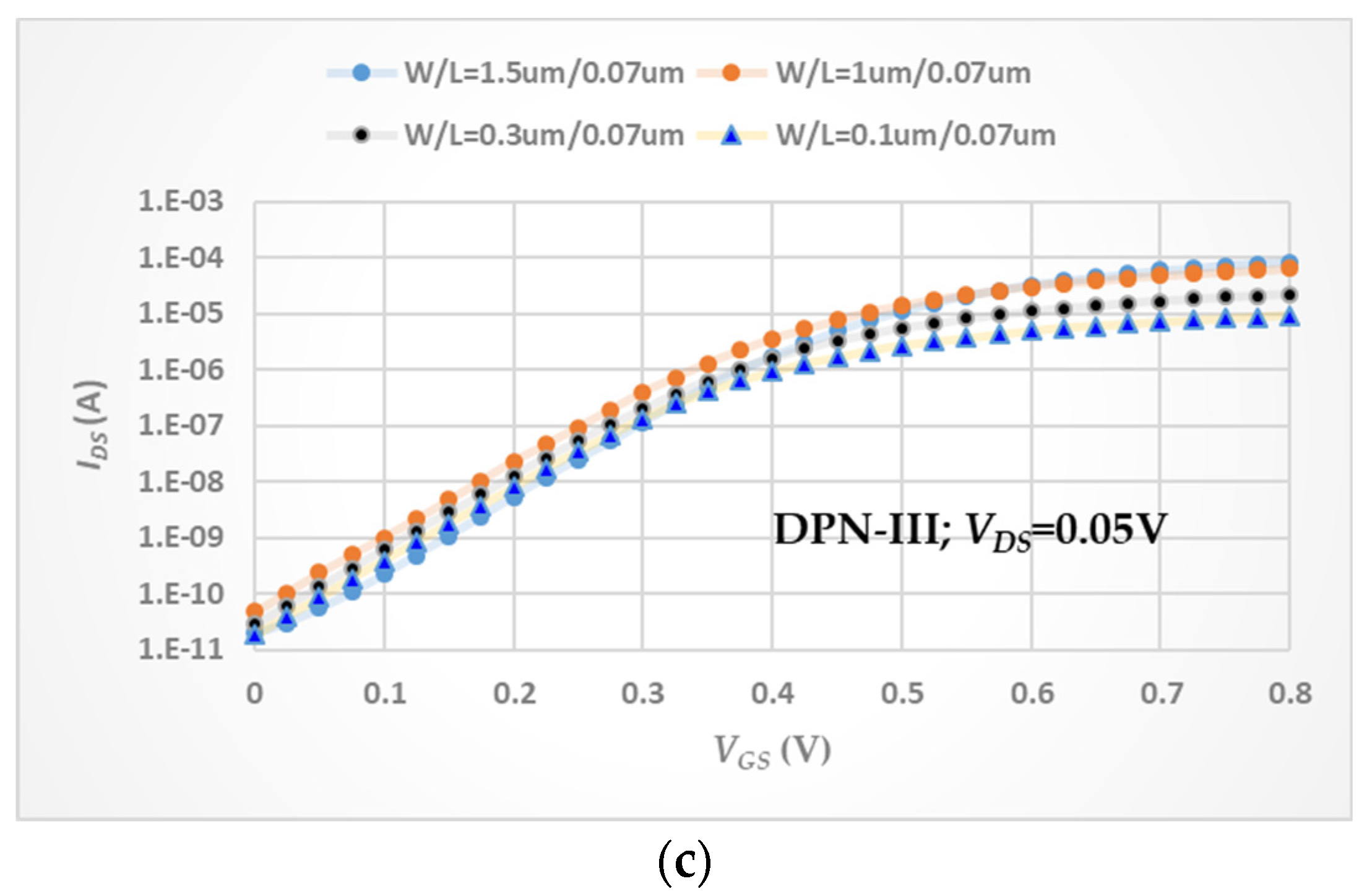
A smaller subthreshold swing indicates better channel control promoting ION/IOFF ratio, which usually means less leakage, and less power consumption. Furthermore, the subthreshold slope is a feature of a MOSFET’s current–voltage characteristics, as shown in Figure 6. In the subthreshold region, the drain current behavior controlled by the gate electrode is analogous to the exponentially decreasing current of a forward biased diode. Thus, a plot of drain current versus gate voltage at fixed drain, source, and bulk voltages will represent nearly a log linear action in this MOSFET operating regime. As described by Equation (6), the ideal minimum SS value is about 60 mV/decade. Thus, using a FinFET device in manufacturing is a feasible choice to achieve the smaller SS values, around 70 mV/decade, quoting from the Reference [9], with high-k gate dielectric. However, if the surface roughness was not well formed, the SS values were still somewhat enlarged with a SiO2/SiON gate dielectric, as described in the Reference [6]. The final consequences of SS values with different tested devices are exhibited in Table 7. The SS value is also a good index for explaining the degree of interfacial defects. A lower SS value means better interface integrity. Most of the SS values in the DPN-I treatment showed a larger SS value as the tested device is fixed and these values in DPN-I are greater than those in other two. In the overall results, the SS value of DPN-III at W/L = 1.5/0.07 (μm/μm) was the smallest. The hypothesis is that the higher nitrogen concentration provides more repair capability in bulk traps of high-k gate dielectric and relatively increases the gate capacitance [17]. This can be inferred from the ION current, as shown in Table 3.
For the DIBL effect, the desired value is as small as possible. As claimed by the published literature [37], a DIBL value close to 30 mV/V is more desirable, but a value of less than 100 mV/V still acceptable in logic circuit design. In terms of the calculated data, the higher DIBL values belong to the larger channel width (W = 1.5 μm) with DPN-II and DPN–III. The possible reason for this is that the higher thermal budget, or higher nitrogen concentration, degrades the surface interface integrity and partially enlarges the VT value at lower VD bias, as shown at Table 8. Because the channel length L is ranged at the nano scale, the DIBL effect is, of course, a bit serious to measure.
In circuit design, pursuing HPC ICs is a target for increasing execution speed and reducing power consumption. However, if the designers need the smaller drive current to retard the speed of circuit module, using the layout technology with narrow channel-width devices is a helpful approach. Hence, revealing the electrical characteristics of nano-node channel-width devices is necessary, especially for high-k/metal gate dielectric with nitrogen treatments. In light of these electrical analyses, electrical performance is strongly related to the geometric size of the gate terminal, allowing doping uniformity and repair performance in high-k dielectric, and to the thermal budget and the nitrogen concentration in the treatment. There is a minor contribution from the uniform controllability of the photolithography and etching technology when forming the desired W/L sizes. As a result, the trend of ION values in Table 3 does not fully follow the ratio of W/L due to the variation of the VT factor. The VT extraction with constant-current method shows the 100-nA coefficient, referred to as C. Hu’s recommendation [30]. In the view of commercial companies, this coefficient for nMOSFET or p-channel MOSFET is little tuned to fit the consideration of standby current in ICs. However, following the specially defined coefficient, the VT difference after data extraction between both transistors is less than 25 mV. For the extremely small VT value, this difference may be important, but for most devices, this difference can be ignored.
According to the electrical performance of the channel-width devices with DPN treatments, on the whole, DPN-I treatment, providing the smallest thermal budget, seems better than the others.
4. Conclusions
Most of the electrical variables for channel-width nMOSFETs at a fixed channel length reveal the electrical performance under different DPN treatments. Besides the top-view contour of gate size possibly influencing the uniformity of nitrogen doping concentration, and indirectly affecting the VT and SS value, the lower thermal budget in nitridation treatment seems to better benefit the major electrical performance. The heavier nitrogen concentration probably causes the worse integrity of channel surface interface, and indirectly increases the VT values as well as reduces the drive current. In the end, the roll-off effect of channel-width devices is also evident, to a small extent, due to oxide thinning at the corner of the AA zone. In the future work, the reliability of channel-width effect devices under nitridation treatments will be an important area of investigation for solid-device applications.
Author Contributions
Conceptualization, S.-Y.C.; methodology, W.-H.L.; formal analysis, all; data curation, Z.-W.Z.; writing—original draft preparation, M.-C.W.; writing—review and editing, S.-K.F.; project administration, M.-C.W. All authors have read and agreed to the published version of the manuscript.
Funding
This research received no external funding.
Acknowledgments
The authors sincerely thank UMC in Taiwan for providing 12” wafers and wish to express their gratitude for the financial support of the Ministry of Science and Technology of Republic of China under Contract MOST 110-2622-E-159-006-CC2.
Conflicts of Interest
The authors declare no conflict of interest.
References
- Ina, H.; Kasumi, K.; Kawakami, E.; Uda, K. Critical issues study of nano-imprint tool for semiconductor volume production. In Proceedings of the SPIE 6517, Emerging Lithographic Technologies XI, San Jose, CA, USA, 25 February–2 March 2007; Volume 6517. [Google Scholar] [CrossRef]
- New Way to Up Chip Yield from Semiconductor Wafer. Available online: https://scienceblog.com/528839/new-way-to-up-chip-yield-from-semiconductor-wafer (accessed on 12 July 2022).
- Unleashing the Future of Innovation. Available online: https://research.tsmc.com/assets/download/Chairman_2021_ISSCC.pdf (accessed on 22 June 2022).
- Moroz, V.; Huang, J.; Choi, M. FinFET/nanowire design for 5nm/3nm technology nodes: Channel cladding and introducing a “bottleneck” shape to remove performance bottleneck. In Proceedings of the IEEE Electron Devices Technology and Manufacturing Conference, Toyama, Japan, 28 February–2 March 2017. [Google Scholar] [CrossRef]
- New Transistor Structures at 3nm/2nm. Available online: https://semiengineering.com/new-transistor-structures-at-3nm-2nm// (accessed on 20 July 2022).
- Wang, M.; Hsieh, W.; Lin, C.; Chu, W.; Liao, W.; Lan, W. High-drain field impacting channel-length modulation effect for nano-node n-channel FinFETs. Crystals 2021, 11, 262. [Google Scholar] [CrossRef]
- Liaw, Y.; Liao, W.; Wang, M.; Lin, C.; Zhou, B.; Gu, H.; Li, D.; Zou, X. A high aspect ratio silicon-fin FinFET fabricated upon SOI wafer. Solid-State Electron. 2016, 126, 46–50. [Google Scholar] [CrossRef]
- Lee, J.C.; Cho, H.J.; Kang, C.S.; Rhee, S.; Kim, Y.H.; Choi, R.; Kang, C.Y.; Choi, C.; Abkar, M. High-k dielectrics and MOSFET characteristics. In Proceedings of the IEEE International Electron Devices Meeting, Washington, DC, USA, 8–10 December 2003. [Google Scholar] [CrossRef]
- Aditya, M.; Rao, K.S.; Sravani, K.G.; Guha, K. Simulation and drain current performance analysis of high-k gate dielectric FinFET. Silicon 2022, 14, 4075–4078. [Google Scholar] [CrossRef]
- Intel Introduces New RibbonFET and PowerVia Technologies. Available online: https://www.youtube.com/watch?v=Rt-7c9Wgnds/ (accessed on 20 July 2022).
- MBCFET—Multi-Bridge Channel FET. Available online: https://samsungatfirst.com/mbcfet/ (accessed on 12 June 2022).
- Seon, Y.; Chang, J.; Yoo, C.; Jeon, J. Device and circuit exploration of multi-nanosheet transistor for Sub-3 nm technology node. Electronics 2021, 10, 180. [Google Scholar] [CrossRef]
- Lee, K.-S.; Park, J.-Y. N-Type nanosheet FETs without ground plane region for process simplification. Micromachines 2022, 13, 432. [Google Scholar] [CrossRef]
- Chin, A.; Lin, B.C.; Chen, W.J.; Lin, Y.B.; Tsai, C. The effect of native oxide on thin gate oxide integrity. IEEE Electron Dev. Lett. 1988, 19, 426–428. [Google Scholar] [CrossRef] [Green Version]
- Chang, H.W.; Huang, P.K.; Yeh, J.W.; Davison, A.; Tsau, C.H.; Yang, C.C. Influence of substrate bias, deposition temperature and post-deposition annealing on the structure and properties of multi-principal-component (AlCrMoSiTi)N coatings. Surf. Coat. Technol. 2008, 202, 3360–3366. [Google Scholar] [CrossRef]
- Lim, S.W.; Luo, T.Y.; Jiang, J. Mechanism of silicon dioxide decoupled plasma nitridation. Jpn. J. Appl. Phys. 2006, 45, L413–L415. [Google Scholar] [CrossRef]
- Chen, C.-W.; Wang, S.-J.; Hsieh, W.-C.; Chen, J.-M.; Jong, T.; Lan, W.-H.; Wang, M.-C. Q-Factor performance of 28 nm-node high-k gate dielectric under DPN treatment at different annealing temperatures. Electronics 2020, 9, 2086. [Google Scholar] [CrossRef]
- Chao, S.-Y.; Huang, H.-S.; Huang, P.-R.; Lin, C.-Y.; Wang, M.-C. Channel mobility model of nano-node MOSFETs incorporating drain-and-gate electric fields. Crystals 2022, 12, 295. [Google Scholar] [CrossRef]
- Asif, R.M.; Rehman, S.U.; Rehman, A.U.; Bajaj, M.; Choudhury, S.; Dash, T.P. A Comparative Study of Short Channel Effects in 3-D FinFET with High-K Gate Di-electric. In Proceedings of the IEEE International Conference in Advances in Power, Signal, and Information Technology, Bhubaneswar, India, 8–10 October 2021. [Google Scholar] [CrossRef]
- Wang, S.J.; Wang, M.C.; Chen, S.Y.; Lan, W.H.; Yang, B.W.; Huang, L.S.; Liu, C.H. Heat stress exposing performance of deep-nano HK/MG nMOSFETs using DPN or PDA treatment. Microelectron. Reliab. 2015, 55, 2203–2207. [Google Scholar] [CrossRef]
- Xia, S.; Shi, Z.; Sun, L.; Sun, S.; Dastan, D.; Fan, R. Suppressing the loss and enhancing the breakdown strengths of high-k materials via constructing layered structure. Mater. Lett. 2022, 312, 131654–131657. [Google Scholar] [CrossRef]
- MacMillen, D.; Butts, M.; Camposano, R.; Hill, D.; Williams, T.W. An industrial view of electronic design automation. IEEE Trans. Comput.-Aided Des. Integr. Circuits Syst. 2000, 19, 1428–1448. [Google Scholar] [CrossRef] [Green Version]
- Xiao, H. Introduction to Semiconductor Manufacturing Technology, 2nd ed.; SPIE: Bellingham, DC, USA, 2012. [Google Scholar]
- Integrating High-k/Metal Gates: Gate-First or Gate-Last? Available online: https://sst.semiconductor-digest.com/2010/03/integrating-high-k/ (accessed on 12 June 2022).
- Wenger, C.; Lukosius, M.; Costina, I.; Sorge, R.; Dabrowski, J.; Müssig, H.J.; Pasko, S.; Lohe, C. Investigation of atomic vapour deposited TiN/HfO2/SiO2 gate stacks for MOSFET devices. Microelectron. Eng. 2008, 85, 1762–1765. [Google Scholar] [CrossRef]
- Dong, M.; Zhang, Y.; Hang, T.; Li, M. Structural effect of inhibitors on adsorption and desorption behaviors during copper electroplating for through-silicon vias. Electrochim. Acta 2021, 372, 137907. [Google Scholar] [CrossRef]
- Shie, K.-C.; Hsu, P.-N.; Li, Y.-J.; Tran, D.-P.; Chen, C. Failure Mechanisms of Cu–Cu Bumps under Thermal Cycling. Materials 2021, 14, 5522. [Google Scholar] [CrossRef]
- Kranti, A.; Armstrong, G.A. Source/Drain Extension Region Engineering in FinFETs for Low-Voltage Analog Applications. IEEE Electron Dev. Lett. 2007, 28, 139–141. [Google Scholar] [CrossRef]
- Jiang, L.; Wen, S.; Tai, W.; Lei, W.; Chang, L.; Cheng, Y. Device parameter variations of n-MOSFETS with dog-bone layouts in 65nm and 40nm technologies. In Proceedings of the IEEE 10th International Conference on ASIC, Shenzhen, China, 28–31 October 2013. [Google Scholar] [CrossRef]
- Hu, C. Modern Semiconductor Devices for Integrated Circuits, 1st ed.; Pearson: Hoboken, NJ, USA, 2010. [Google Scholar]
- Streetman, B.G.; Banerjee, S.K. Solid State Electronic Devices, 7th ed.; Pearson: Hoboken, NJ, USA, 2016. [Google Scholar]
- Bucher, M.; Makris, N.; Chevas, L. Generalized constant current method for determining MOSFET threshold voltage. IEEE Trans. Electron Dev. 2020, 67, 4559–4562. [Google Scholar] [CrossRef]
- Transconductance. Available online: https://en.wikipedia.org/wiki/Transconductance (accessed on 12 June 2022).
- Subthreshold Slope. Available online: https://en.wikipedia.org/wiki/Subthreshold_slope (accessed on 12 June 2022).
- Tsormpatzoglou, A.; Dimitriadis, C.A.; Clerc, R.; Pananakakis, G.; Ghibaudo, G. Threshold voltage model for short-channel undoped symmetrical double-gate MOSFETs. IEEE Trans. Electron Dev. 2008, 55, 2512–2516. [Google Scholar] [CrossRef]
- Hook, T.B.; Biesemans, S.; Slinkman, J. The dependence of channel length on channel width in narrow-channel CMOS devices for 0.35–0.13 μm technologies. IEEE Electron Dev. Lett. 2000, 21, 85–87. [Google Scholar] [CrossRef]
- Chen, X.; Ouyang, Q.; Wang, G.; Banerjee, S. Improved hot carrier and short channel performance in vertical nMOSFETs with graded channel doping. IBM Res. Rep. 2002, 49, 1962–1968. [Google Scholar]
Figure 1.
The schematic MOSFET with high-k/metal gate formation: (a) top-view layout as W1 > W2 > W3 and (b) cross-sectional profile.
Figure 1.
The schematic MOSFET with high-k/metal gate formation: (a) top-view layout as W1 > W2 > W3 and (b) cross-sectional profile.
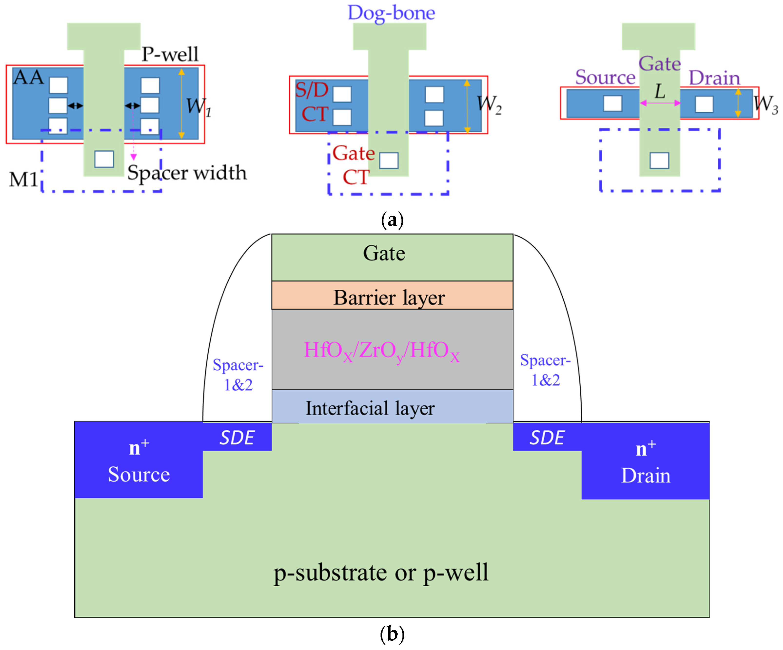
Figure 2.
Electrical performance of ID–VD curves for four tested nMOSFETs (a) with DPN-I treatment, (b) with DPN-II treatment, and (c) with DPN-III treatment.
Figure 2.
Electrical performance of ID–VD curves for four tested nMOSFETs (a) with DPN-I treatment, (b) with DPN-II treatment, and (c) with DPN-III treatment.

Figure 3.
Electrical characteristics of ID–VD curves exposing OFF-state current (a) with DPN-I treatment, (b) with DPN-II treatment, and (c) with DPN-III treatment.
Figure 3.
Electrical characteristics of ID–VD curves exposing OFF-state current (a) with DPN-I treatment, (b) with DPN-II treatment, and (c) with DPN-III treatment.

Figure 4.
VT variables under different VD operations (a) with DPN-I treatment, (b) with DPN-II treatment, (c) with DPN-III treatment and (d) with channel-width effect at VD = 0.05 V and L = 0.07 μm.
Figure 4.
VT variables under different VD operations (a) with DPN-I treatment, (b) with DPN-II treatment, (c) with DPN-III treatment and (d) with channel-width effect at VD = 0.05 V and L = 0.07 μm.
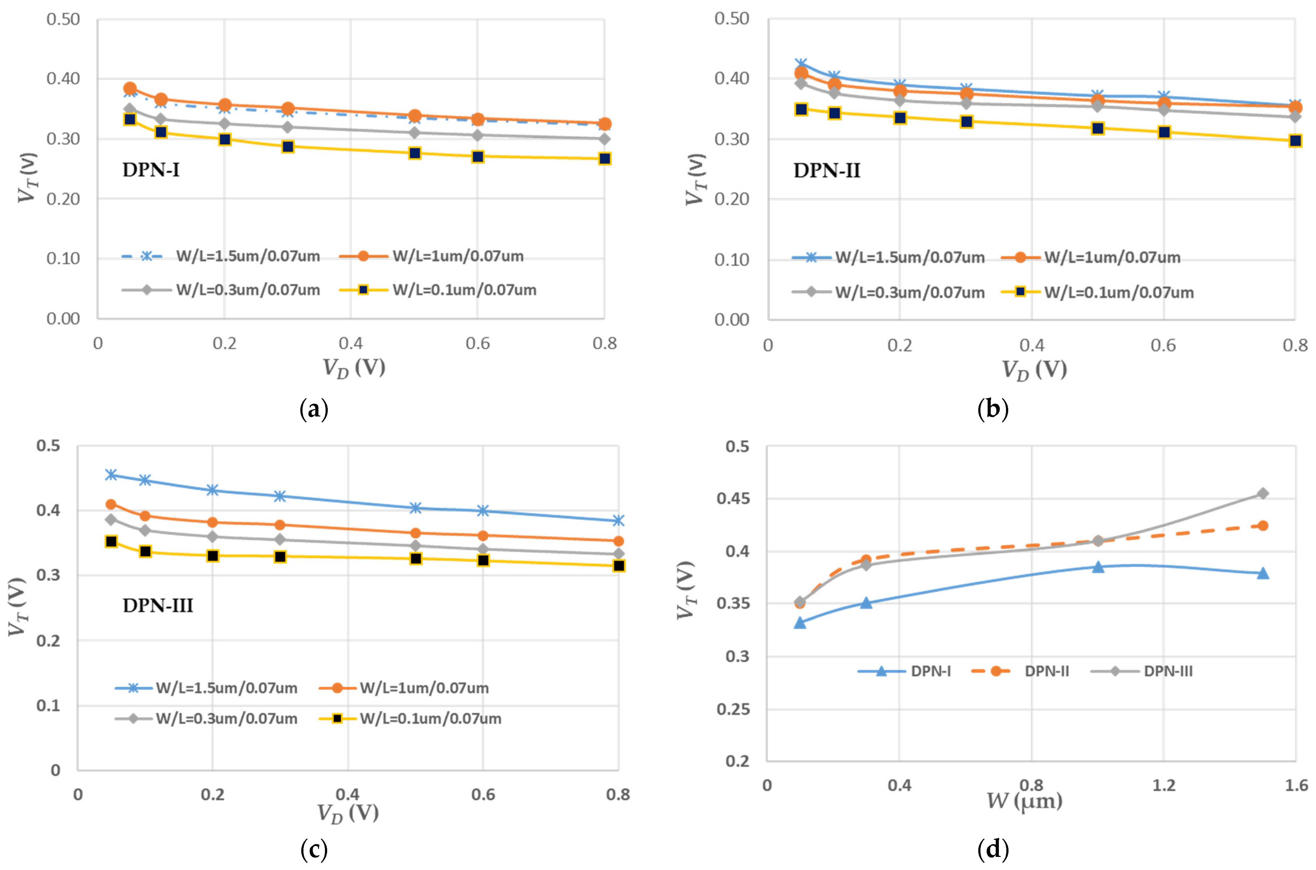
Figure 5.
Gm characteristics (a) with DPN-I treatment, (b) with DPN-II treatment, and (c) with DPN-III treatment.
Figure 5.
Gm characteristics (a) with DPN-I treatment, (b) with DPN-II treatment, and (c) with DPN-III treatment.

Figure 6.
IDS vs. VGS performance with log-scale and VDS = 0.05 V (a) under DPN-I treatment, (b) under DPN-II treatment, and (c) under DPN-III treatment.
Figure 6.
IDS vs. VGS performance with log-scale and VDS = 0.05 V (a) under DPN-I treatment, (b) under DPN-II treatment, and (c) under DPN-III treatment.


Table 1.
Variables and parameters of gate dielectric deposition with three nitridation treatments.
| No. Wafer | SiO2 (IL) | HfOX/ZrOX/HfOX (Cycle) | Anneal | N2 |
|---|---|---|---|---|
| DPN-I | 9~12 Å | 10/4/10 | 700 °C | 8% |
| DPN-II | 9~12 Å | 10/4/10 | 900 °C | 8% |
| DPN-III | 9~12 Å | 10/4/10 | 700 °C | 16% |
Table 2.
Valuable semiconductor parameters with sensing metrology.
| Parameter Extraction | Sensing Metrology |
|---|---|
| VT | Sensing IDS − VGS as fixed VDS = 50 mV. Extracting the VT value as the expected IDS (nA) = 100 × W/L. |
| ION | Measuring IDS − VDS as fixed VGS = VDD or (VGS−VT) = VDD. Choosing IDS as VDS = VDD. |
| IOFF | Sensing IDS − VDS as VG = VS = VB = 0 V. Recording ID, IG, IS, and IB as VDS = VDD. |
| Gm | Deriving IDS − VGS as fixed VDS = 50 mV. Extracting the maximum Gm_max. |
| SS | Deriving Log(IDS) − VGS as fixed VDS = 50 mV or VDD. Extracting the slope and taking the reciprocal. |
Table 3.
ION (μA) measured at VDS = 0.8 V and VGS = 0.5 V with three DPN treatments.
| Tested Device W/L (μm/μm) | DPN-I | DPN-II | DPN-III |
|---|---|---|---|
| 1.5/0.07 | 77.5 | 75.4 | 81.6 |
| 1/0.07 | 61.5 | 52.2 | 38.4 |
| 0.3/0.07 | 25.7 | 17.9 | 17.6 |
| 0.1/0.07 | 11.7 | 8.37 | 7.17 |
Table 4.
IOFF (pA) measured at VDS = 0.8 V and VGS = 0 V with three DPN treatments.
| Tested Device W/L (μm/μm) | DPN-I | DPN-II | DPN-III |
|---|---|---|---|
| 1.5/0.07 | 602 | 721 | 311 |
| 1/0.07 | 67.7 | 103 | 98.6 |
| 0.3/0.07 | 123 | 119 | 80.8 |
| 0.1/0.07 | 18 | 236 | 45.1 |
Table 5.
VT (V) measured at VDS = 0.05 V and VS = VB = 0 V with three DPN treatments.
| Tested Device W/L (μm/μm) | DPN-I | DPN-II | DPN-III |
|---|---|---|---|
| 1.5/0.07 | 0.380 | 0.425 | 0.455 |
| 1/0.07 | 0.386 | 0.410 | 0.410 |
| 0.3/0.07 | 0.351 | 0.392 | 0.387 |
| 0.1/0.07 | 0.333 | 0.350 | 0.352 |
| 1.5/0.09 | 0.368 | 0.362 | 0.396 |
Table 6.
Gm_max (μS) measured at VDS = 0.05 V and VS = VB = 0 V with three DPN treatments with normalization.
Table 6.
Gm_max (μS) measured at VDS = 0.05 V and VS = VB = 0 V with three DPN treatments with normalization.
| Tested Device W/L (μm/μm) | DPN-I | DPN-II | DPN-III | DPN-I Normalization | DPN-II Normalization | DPN-III Normalization |
|---|---|---|---|---|---|---|
| 1.5/0.07 | 190 | 274 | 267 | 127 | 183 | 178 |
| 1/0.07 | 149 | 175 | 179 | 149 | 175 | 179 |
| 0.3/0.07 | 52.3 | 53.1 | 59.2 | 174 | 177 | 197 |
| 0.1/0.07 | 22.0 | 20.8 | 23.2 | 220 | 208 | 232 |
| 1.5/0.09 | 204 | 235 | 123 | 175 | 202 | 105 |
Table 7.
SS (mV/decade) derived from ID–VG curves at VDS = 0.05 V and VS = VB = 0 V with three DPN treatments.
Table 7.
SS (mV/decade) derived from ID–VG curves at VDS = 0.05 V and VS = VB = 0 V with three DPN treatments.
| Tested Device W/L (μm/μm) | DPN-I | DPN-II | DPN-III |
|---|---|---|---|
| 1.5/0.07 | 85.4 | 81.5 | 74.5 |
| 1/0.07 | 84.8 | 74.9 | 81.8 |
| 0.3/0.07 | 83.9 | 78.9 | 82 |
| 0.1/0.07 | 83 | 82.4 | 79.7 |
| 1.5/0.09 | 84.9 | 83.5 | 80.6 |
Table 8.
DIBL (mV/V) exposing the VT difference at VDS = 0.05 V and VDD with three DPN treatments.
| Tested Device W/L (μm/μm) | DPN-I | DPN-II | DPN-III |
|---|---|---|---|
| 1.5/0.07 | 74.1 | 92.1 | 94.4 |
| 1/0.07 | 79.7 | 75.5 | 76.1 |
| 0.3/0.07 | 67.5 | 73.2 | 71.2 |
| 0.1/0.07 | 87.3 | 70.0 | 49.6 |
Publisher’s Note: MDPI stays neutral with regard to jurisdictional claims in published maps and institutional affiliations. |
© 2022 by the authors. Licensee MDPI, Basel, Switzerland. This article is an open access article distributed under the terms and conditions of the Creative Commons Attribution (CC BY) license (https://creativecommons.org/licenses/by/4.0/).
Share and Cite
MDPI and ACS Style
Chao, S.-Y.; Lan, W.-H.; Fan, S.-K.; Zhon, Z.-W.; Wang, M.-C. Electrical Performance of 28 nm-Node Varying Channel-Width nMOSFETs under DPN Process Treatments. Micromachines 2022, 13, 1861. https://doi.org/10.3390/mi13111861
AMA Style
Chao S-Y, Lan W-H, Fan S-K, Zhon Z-W, Wang M-C. Electrical Performance of 28 nm-Node Varying Channel-Width nMOSFETs under DPN Process Treatments. Micromachines. 2022; 13(11):1861. https://doi.org/10.3390/mi13111861
Chicago/Turabian StyleChao, Shou-Yen, Wen-How Lan, Shou-Kong Fan, Zi-Wen Zhon, and Mu-Chun Wang. 2022. "Electrical Performance of 28 nm-Node Varying Channel-Width nMOSFETs under DPN Process Treatments" Micromachines 13, no. 11: 1861. https://doi.org/10.3390/mi13111861
Note that from the first issue of 2016, this journal uses article numbers instead of page numbers. See further details here.