
A High-Sensitivity Vacuum Diode Temperature Sensor Based on Barrier-Lowering Effect

 ,
,  , ,
, ,
Abstract
:
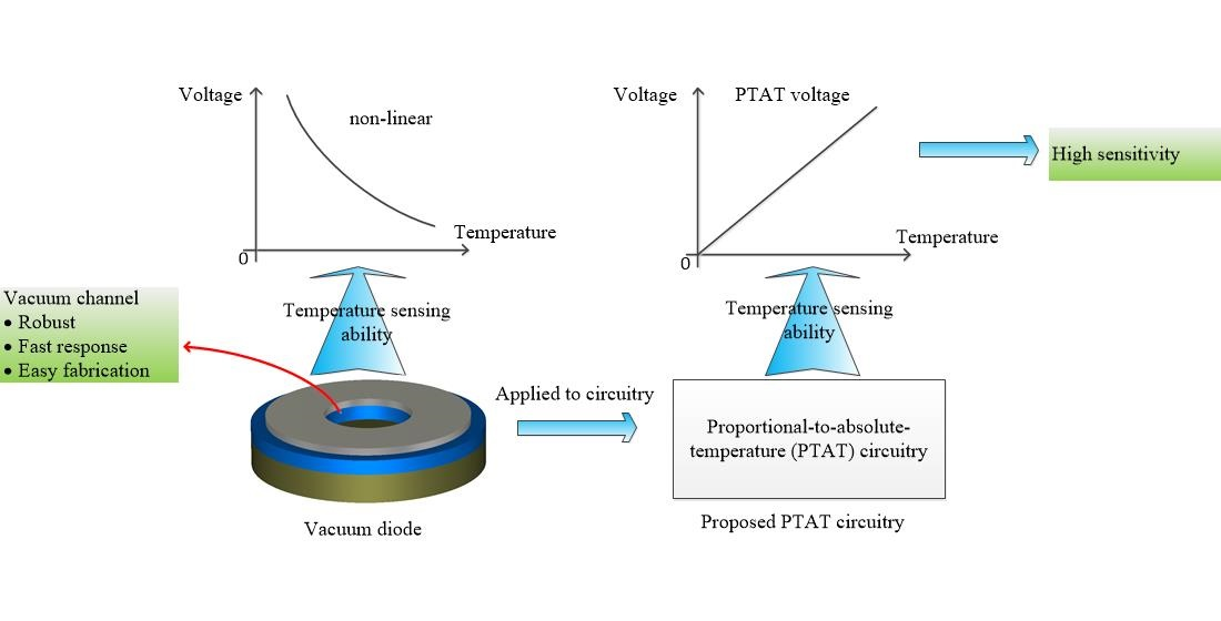
1. Introduction
2. Methods
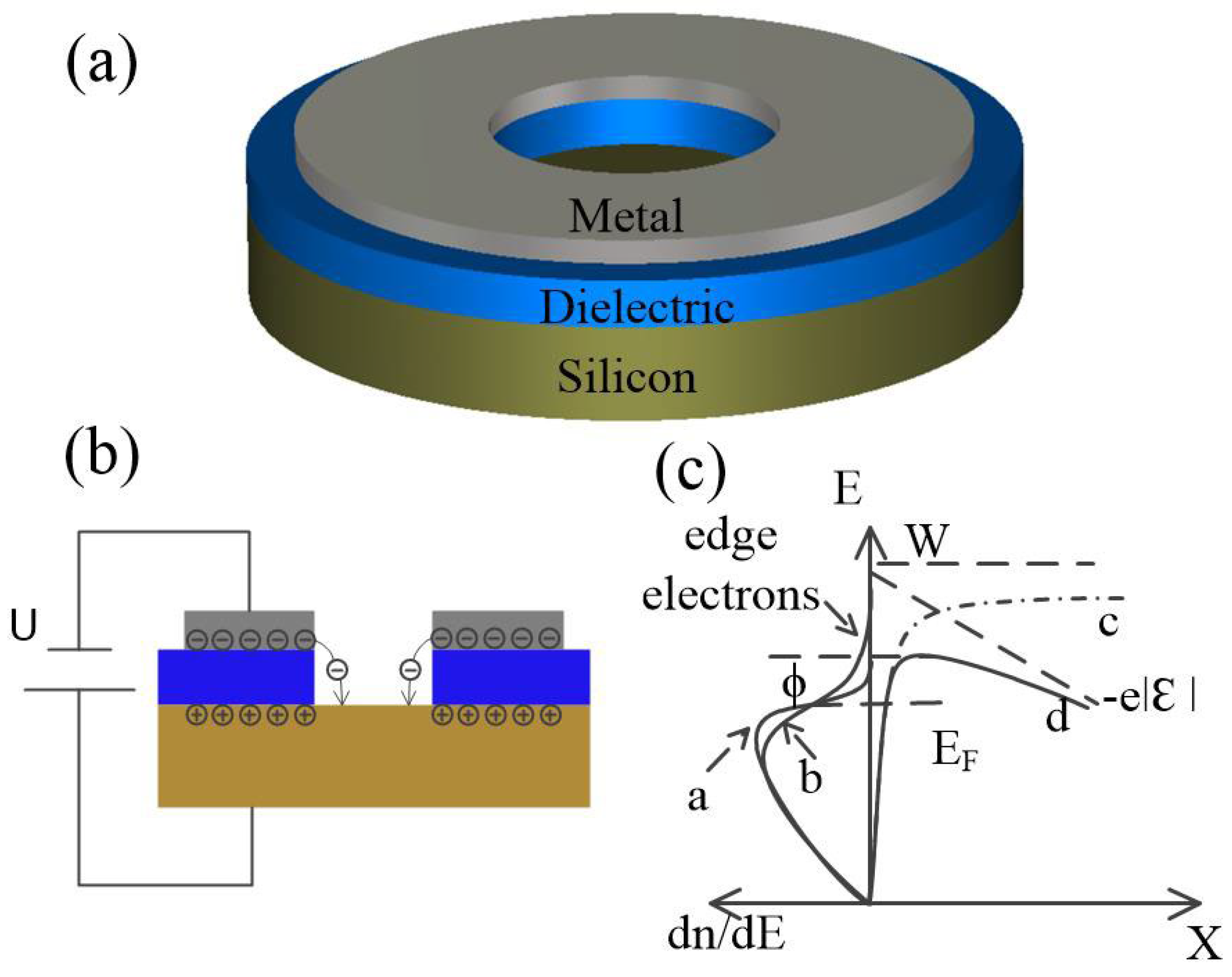
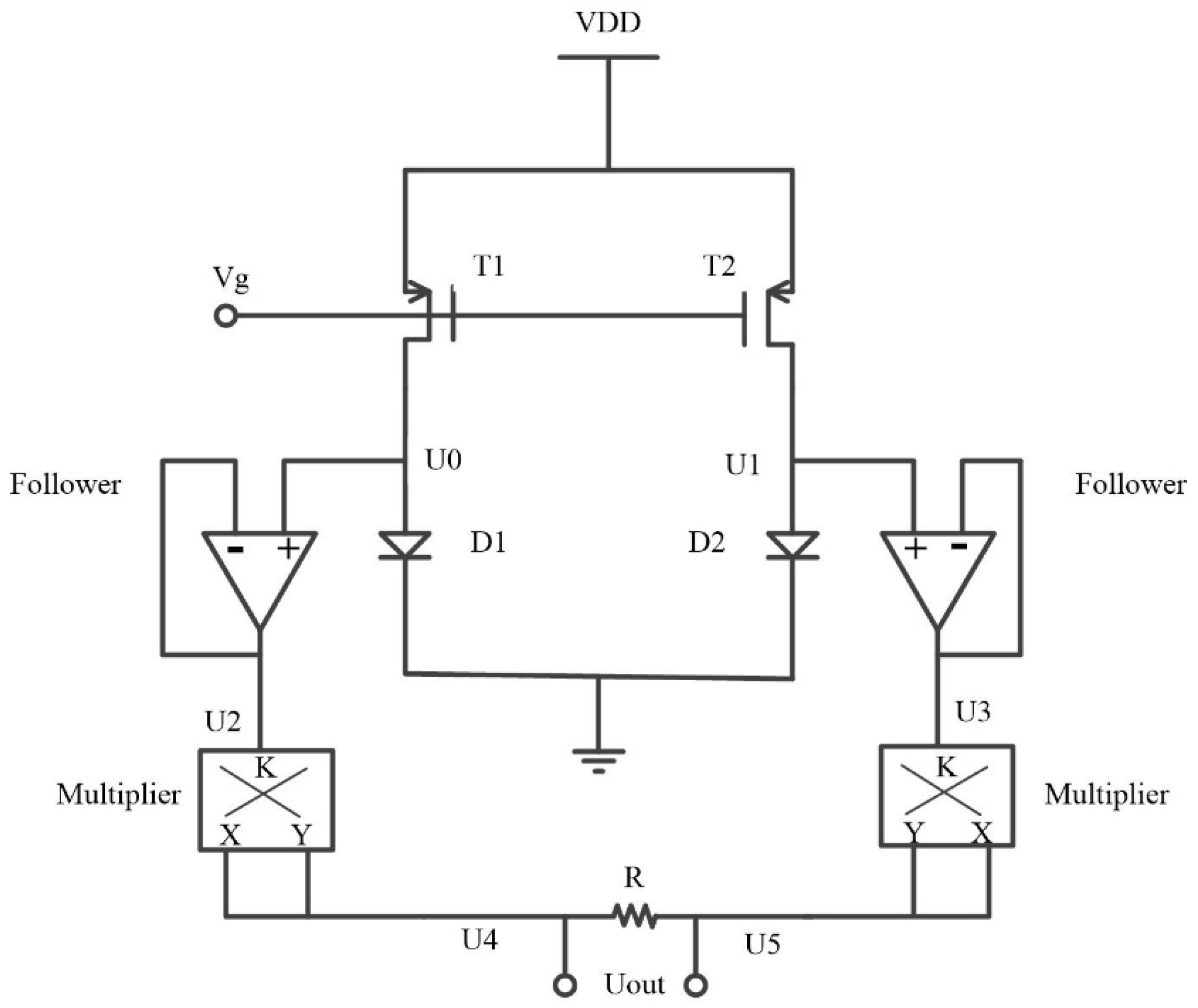
2.1. Device Structure and Working Principle
2.2. Simulation Technique
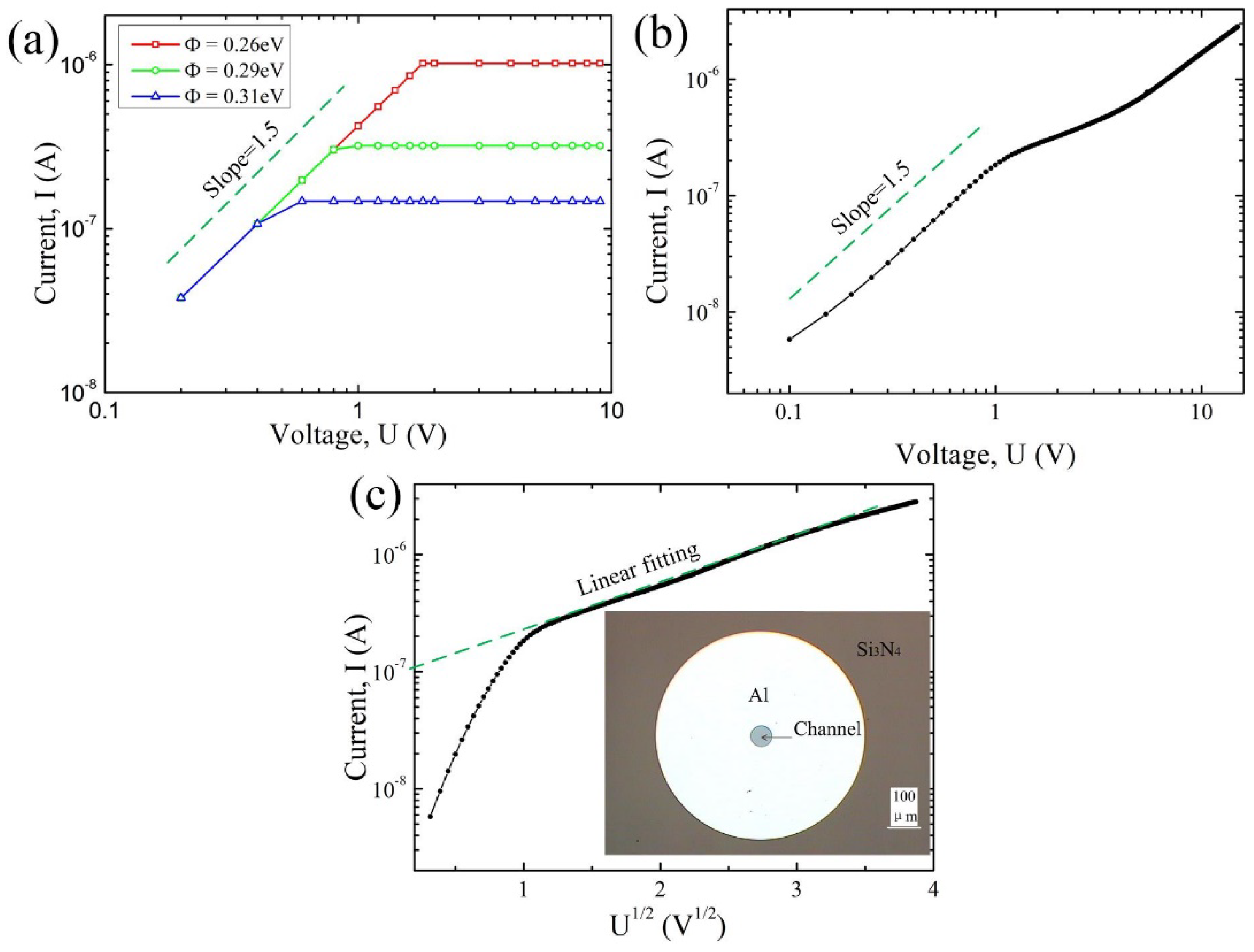
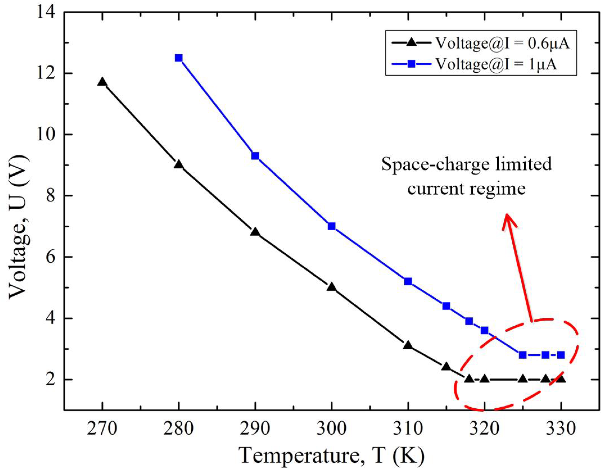
3. Results and Discussion
4. Conclusions
Author Contributions
Funding
Conflicts of Interest
References
- Alemdar, H.; Ersoy, C. Wireless sensor networks for healthcare: A survey. Comput. Netw. 2010, 54, 2688–2710. [Google Scholar] [CrossRef]
- Gungor, V.C.; Hancke, G.P. Industrial Wireless Sensor Networks: Challenges, Design Principles, and Technical Approaches. IEEE Trans. Ind. Electron. 2009, 56, 4258–4265. [Google Scholar] [CrossRef] [Green Version]
- Law, M.K.; Bermak, A.; Luong, H.C. A Sub-μm W Embedded CMOS Temperature Sensor for RFID Food Monitoring Application. IEEE J. Solid-State Circuits 2010, 45, 1246–1255. [Google Scholar] [CrossRef]
- Chen, C.-C.; Lu, W.-F.; Tsai, C.-C.; Chen, P. A time-to-digital-converter-based CMOS smart temperature sensor. IEEE J. Solid-State Circuits 2005, 40, 1642–1648. [Google Scholar] [CrossRef]
- Vroonhoven, C.; D’Aquino, D.; Makinwa, K. A thermal-diffusivity-based temperature sensor with an untrimmed inaccuracy of ±0.2 °C (3s) from −55 °C to 125 °C. In Proceedings of the 2010 IEEE International Solid-State Circuits Conference, San Francisco, CA, USA, 7–11 February 2010. [Google Scholar]
- Ge, G.; Cheng, Z.; Hoogzaad, G.; Makinwa, K. A single-trim CMOS bandgap reference with a 3σ inaccuracy of ±0.15% from −40 °C to 125 °C. In Proceedings of the 2010 IEEE International Solid-State Circuits Conference, San Francisco, CA, USA, 7–11 February 2010. [Google Scholar]
- Makinwa, K.; Snoeij, M.F. A CMOS temperature-to-frequency converter with an inaccuracy of less than ±0.5 °C (3σ) from −40 °C to 105 °C. IEEE J. Solid-State Circuits 2007, 41, 2992–2997. [Google Scholar] [CrossRef]
- Rao, S.; Pangallo, G.; Pezzimenti, F.; Della Corte, F.G. High-Performance Temperature Sensor Based on 4H-SiC Schottky Diodes. IEEE Electron Device Lett. 2015, 36, 720–722. [Google Scholar] [CrossRef]
- Basov, M. Schottky diode temperature sensor for pressure sensor. Sens. Actuators A Phys. 2021, 331, 112930. [Google Scholar] [CrossRef]
- Rao, S.; Benedetto, L.D.; Pangallo, G.; Rubino, A.; Bellone, S.; Della Corte, F.G. 85 K to 440 K Temperature Sensor Based on a 4H-SiC Schottky Diode. IEEE Sens. J. 2016, 16, 6537–6542. [Google Scholar] [CrossRef]
- Li, X.; Pu, T.; Li, X.; Li, L.; Ao, J.P. Correlation Between Anode Area and Sensitivity for the TiN/GaN Schottky Barrier Diode Temperature Sensor. IEEE Trans. Electron. Devices 2020, 67, 1171–1175. [Google Scholar] [CrossRef]
- Kumar, V.; Verma, J.; Maan, A.; Akhtar, J. Epitaxial 4H–SiC based Schottky diode temperature sensors in ultra-low current range. Vacuum 2020, 182, 109590. [Google Scholar] [CrossRef]
- Kumar, V.; Pawar, S.; Maan, A.S.; Akhtar, J. Diameter dependent thermal sensitivity variation trend in Ni/4H-SiC Schottky diode temperature sensors. J. Vac. Sci. Technol. B Nanotechnol. Microelectron. Mater. Processing Meas. Phenom. 2015, 33, 052207. [Google Scholar] [CrossRef]
- Kumar, V.; Maan, A.S.; Akhtar, J. Barrier height inhomogeneities induced anomaly in thermal sensitivity of Ni/4H-SiC Schottky diode temperature sensor. J. Vac. Sci. Technol. B Microelectron. Nanometer Struct. 2014, 32, 041203. [Google Scholar] [CrossRef]
- Zhang, N.; Lin, C.M.; Senesky, D.G.; Pisano, A.P. Temperature sensor based on 4H-silicon carbide pn diode operational from 20 °C to 600 °C. Appl. Phys. Lett. 2014, 104, 073504. [Google Scholar] [CrossRef]
- Shwarts, Y.M.; Borblik, V.L.; Kulish, N.R.; Venger, E.F.; Sokolov, V.N. Limiting characteristics of diode temperature sensors. Sens. Actuators A Phys. 2000, 86, 197–205. [Google Scholar] [CrossRef]
- Rao, S.; Pangallo, G.; Corte, F.D. Highly Linear Temperature Sensor Based on 4H-Silicon Carbide p-i-n Diodes. IEEE Electron Device Lett. 2015, 36, 1205–1208. [Google Scholar] [CrossRef]
- Rao, S.; Pangallo, G.; Corte, F.D. 4H-SiC p-i-n diode as Highly Linear Temperature Sensor. IEEE Trans. Electron Devices 2015, 63, 414–418. [Google Scholar] [CrossRef]
- Li, G.; Andre, N.; Chen, Q.; Wang, H.; Francis, L.A.; Zeng, Y.; Liao, L.; Flandre, D. Low-Power, High-Sensitivity Temperature Sensor Based on Ultrathin SOI Lateral p-i-n Gated Diode. Electron Devices. IEEE Trans. Electron Devices 2019, 66, 4001–4007. [Google Scholar] [CrossRef]
- Han, J.W.; Seol, M.L.; Meyyappan, M. Nanoscale vacuum field emission gated diode with an umbrella cathode. Nanoscale Adv. 2021, 3, 1725–1729. [Google Scholar] [CrossRef]
- Wang, X.; Xue, T.; Shen, Z.; Long, M.; Wu, S. Analysis of the electron emission characteristics and working mechanism of a planar bottom gate vacuum field emission triode with a nanoscale channel. Nanoscale 2021, 13, 14363–14370. [Google Scholar] [CrossRef]
- Liu, M.; Liang, S.; Shi, D.; Yang, S.; Lei, Y.; Li, T.; Wang, Y. An emission stable vertical air channel diode by a low-cost and IC compatible BOE etching process. Nanoscale 2021, 13, 5693–5699. [Google Scholar] [CrossRef] [PubMed]
- Zhou, S.; Chen, K.; Guo, X.; Cole, M.T.; Wu, Y.; Li, Z.; Zhang, S.; Li, C.; Dai, Q. Antenna-coupled vacuum channel nano-diode with high quantum efficiency. Nanoscale 2020, 12, 1495–1499. [Google Scholar] [CrossRef] [PubMed]
- Srisonphan, S.; Jung, Y.S.; Kim, H.K. Metal–oxide–semiconductor field-effect transistor with a vacuum channel. Nat. Nanotechnol. 2012, 7, 504–508. [Google Scholar] [CrossRef] [PubMed]
- Wu, G.; Wei, X.; Gao, S.; Chen, Q.; Peng, L.-M. Tunable graphene micro-emitters with fast temporal response and controllable electron emission. Nat. Commun. 2016, 7, 1–8. [Google Scholar] [CrossRef] [PubMed] [Green Version]
- Shen, Z.; Wang, X.; Wu, S.; Tian, J. A new kind of vertically aligned field emission transistor with a cylindrical vacuum channel. Vacuum 2017, 137, 163–168. [Google Scholar] [CrossRef]
- Ando, T.; Fowler, A.B.; Stern, F. Electronic properties of two-dimensional systems. Rev. Mod. Phys. 1982, 104, 073504. [Google Scholar] [CrossRef]
- Shen, Z.; Li, Q.; Wang, X.; Tian, J.; Wu, S. Nanoscale Vacuum Diode Based on Thermionic Emission for High Temperature Operation. Micromachines 2021, 12, 729. [Google Scholar] [CrossRef]

Publisher’s Note: MDPI stays neutral with regard to jurisdictional claims in published maps and institutional affiliations. |
© 2022 by the authors. Licensee MDPI, Basel, Switzerland. This article is an open access article distributed under the terms and conditions of the Creative Commons Attribution (CC BY) license (https://creativecommons.org/licenses/by/4.0/).
Share and Cite
Shen, Z.; Wang, X.; Li, Q.; Ge, B.; Jiang, L.; Tian, J.; Wu, S. A High-Sensitivity Vacuum Diode Temperature Sensor Based on Barrier-Lowering Effect. Micromachines 2022, 13, 286. https://doi.org/10.3390/mi13020286
Shen Z, Wang X, Li Q, Ge B, Jiang L, Tian J, Wu S. A High-Sensitivity Vacuum Diode Temperature Sensor Based on Barrier-Lowering Effect. Micromachines. 2022; 13(2):286. https://doi.org/10.3390/mi13020286
Chicago/Turabian StyleShen, Zhihua, Xiao Wang, Qiaoning Li, Bin Ge, Linlin Jiang, Jinshou Tian, and Shengli Wu. 2022. "A High-Sensitivity Vacuum Diode Temperature Sensor Based on Barrier-Lowering Effect" Micromachines 13, no. 2: 286. https://doi.org/10.3390/mi13020286