
Long-Term Accuracy Enhancement of Binary Neural Networks Based on Optimized Three-Dimensional Memristor Array

 ,
, 
Abstract
:1. Introduction
2. Experiment
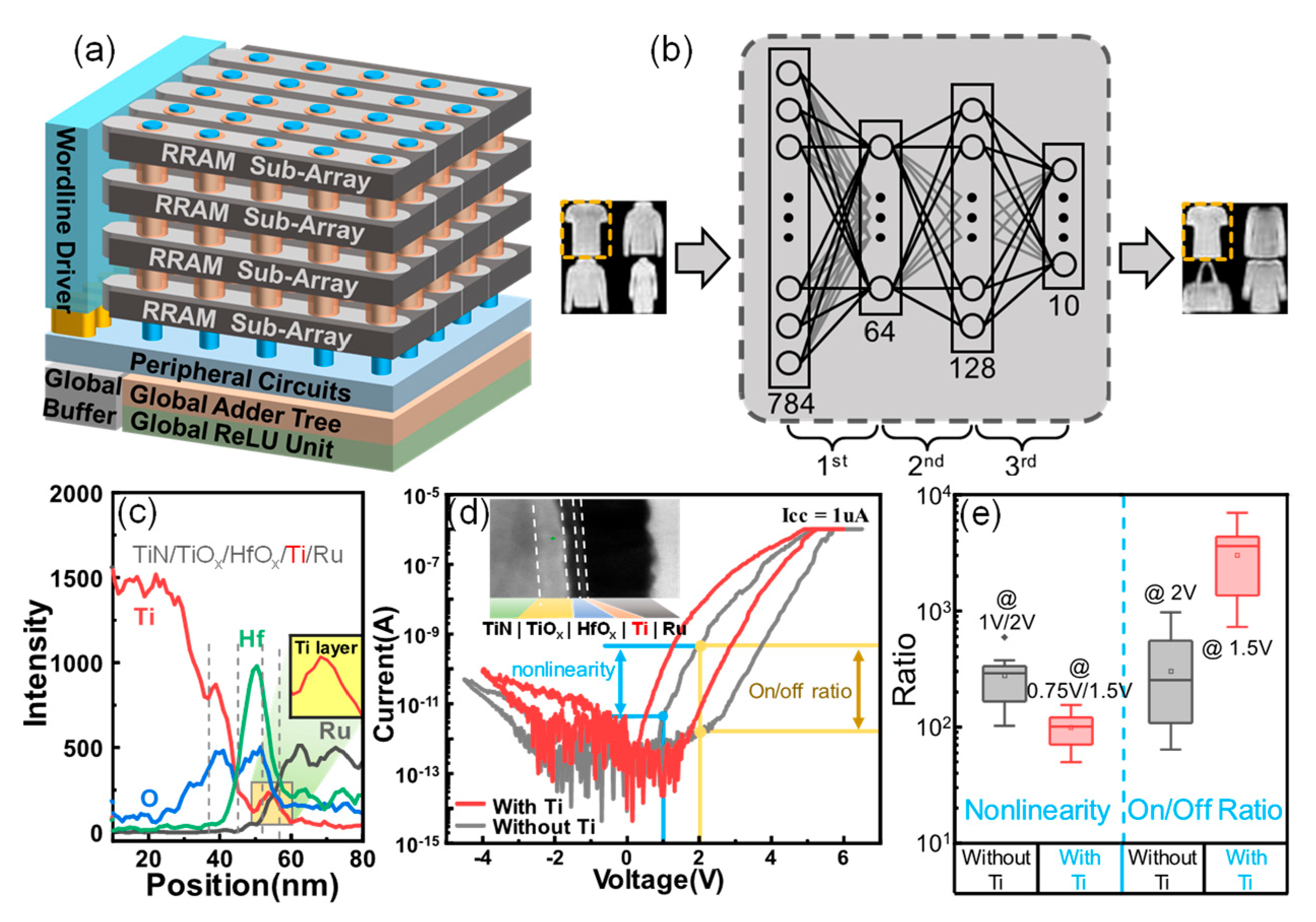
3. Results
4. Discussion
5. Conclusions
Author Contributions
Funding
Institutional Review Board Statement
Informed Consent Statement
Data Availability Statement
Conflicts of Interest
References
- Zhu, S.; Ota, K.; Dong, M. Energy efficient artificial intelligence of things with intelligent edge. IEEE Internet Things J. 2022. [Google Scholar] [CrossRef]
- Zhang, W.E.; Sheng, Q.Z.; Mahmood, A.; Zaib, M.; Hamad, S.A.; Aljubairy, A.; Alhazmi, A.A.F.; Sagar, S.; Ma, C. The 10 Research Topics in the Internet of Things. In Proceedings of the 2020 IEEE 6th International Conference on Collaboration and Internet Computing (CIC), Atlanta, GA, USA, 1–3 December 2020. [Google Scholar]
- Farhan, L.; Kharel, R.; Kaiwartya, O.; Quiroz-Castellanos, M.; Alissa, A.; Abdulsalam, M. A Concise Review on Internet of Things (Iot)—Problems, Challenges and Opportunities. In Proceedings of the 2018 11th International Symposium on Communication Systems, Networks & Digital Signal Processing (CSNDSP), Budapest, Hungary, 18–20 July 2018; pp. 1–6. [Google Scholar]
- Khayyam, H.; Javadi, B.; Jalili, M.; Jazar, R.N. Artificial Intelligence and Internet of Things for Autonomous Vehicles. In Nonlinear Approaches in Engineering Applications; Springer: Cham, Switzerland, 2020; pp. 39–68. [Google Scholar]
- Dananjaya, P.A.; Gopalakrishnan, R.; Lew, W.S. RRAM-based neuromorphic computing systems. In Emerging Non-Volatile Memory Technologies; Springer: Singapore, 2021; pp. 383–414. [Google Scholar]
- Xia, Q.; Yang, J.J. Memristive crossbar arrays for brain-inspired computing. Nat. Mater. 2019, 18, 309–323. [Google Scholar] [CrossRef] [PubMed]
- Sebastian, A.; Le Gallo, M.; Khaddam-Aljameh, R.; Eleftheriou, E. Memory devices and applications for in-memory computing. Nat. Nanotechnol. 2020, 15, 529–544. [Google Scholar] [CrossRef] [PubMed]
- Yao, P.; Wu, H.; Gao, B.; Tang, J.; Zhang, Q.; Zhang, W.Q.; Yang, J.J.; Qian, H. Fully hardware-implemented memristor convolutional neural network. Nature 2020, 577, 641–646. [Google Scholar] [CrossRef] [PubMed]
- Zidan, M.A.; Strachan, J.P.; Lu, W.D. The future of electronics based on memristive systems. Nat. Electron. 2018, 1, 22–29. [Google Scholar] [CrossRef]
- Xu, X.; Ding, Y.; Hu, S.X.; Niemier, M.; Cong, J.; Hu, Y.; Shi, Y. Scaling for edge inference of deep neural networks. Nat. Electron. 2018, 1, 216–222. [Google Scholar] [CrossRef]
- Zhao, M.; Wu, H.; Gao, B.; Zhang, Q.; Wu, W.; Wang, S.; Xi, Y.; Wu, D.; Deng, N.; Yu, S.; et al. Investigation of Statistical Retention of Filamentary Analog RRAM for Neuromorphic Computing. In Proceedings of the 2017 IEEE International Electron Devices Meeting (IEDM), San Francisco, CA, USA, 2–6 December 2017; Volume 39, pp. 4.1–4.4. [Google Scholar]
- Lammie, C.; Eshraghian, J.K.; Li, C.; Amirsoleimani, A.; Genov, R.; Lu, W.D.; Azghadi, M.R. Design space exploration of dense and sparse mapping schemes for rram architectures. arXiv 2022, arXiv:2201.06703. [Google Scholar]
- Courbariaux, M.; Hubara, I.; Soudry, D.; El-Yaniv, R.; Bengio, Y. Binarized neural networks: Training deep neural networks with weights and activations constrained to +1 or −1. arXiv 2016, arXiv:1602.02830. [Google Scholar]
- Kim, B.; Hanson, E.; Li, H. An efficient 3d reram convolution processor design for binarized weight networks. IEEE Trans. Circuits Syst. II Express Briefs 2021, 68, 1600–1604. [Google Scholar] [CrossRef]
- Zayer, F.; Lahbacha, K.; Dghais, W.; Belgacem, H.; de Magistris, M.; Maffucci, A.; Melnikov, A.V. Thermal and Signal Integrity Analysis of Novel 3d Crossbar Resistive Random Access Memories. In Proceedings of the 2019 IEEE 23rd Workshop on Signal and Power Integrity (SPI), Chambery, France, 18–21 June 2019; pp. 1–4. [Google Scholar]
- Chen, P.; Li, Z.; Yu, S. Design trade-offs of vertical RRAM-based 3-D cross-point array. IEEE Trans. Very Large Scale Integr. Syst. 2016, 24, 3460–3467. [Google Scholar] [CrossRef]
- Luo, Q.; Zhang, X.; Hu, Y.; Gong, T.; Xu, X.; Yuan, P.; Ma, H.; Dong, D.; Lv, H.; Long, S.; et al. Self-rectifying and forming-free resistive-switching device for embedded memory application. IEEE Electron Device Lett. 2018, 39, 664–667. [Google Scholar] [CrossRef]
- Wang, Z.; Kang, J.; Bai, G.; Zhong, G.; Wang, B.; Ling, Y.; Chen, Q.; Bao, L.; Wu, L.; Cai, Y.; et al. Self-selective resistive device with hybrid switching mode for passive crossbar memory application. IEEE Electron Device Lett. 2020, 41, 1009–1012. [Google Scholar] [CrossRef]
- Xu, X.; Luo, Q.; Gong, T.; Lv, H.; Long, S.; Liu, Q.; Chung, S.; Li, J.; Liu, M. Fully CMOS compatible 3D vertical RRAM with self-aligned self-selective cell enabling sub-5nm scaling. In Proceedings of the 2016 IEEE Symposium on VLSI Technology, Honolulu, HI, USA, 14–16 June 2016; pp. 1–2. [Google Scholar]
- Lee, S.; Lee, D.; Woo, J.; Cha, E.; Park, J.; Hwang, H. Engineering oxygen vacancy of tunnel barrier and switching layer for both selectivity and reliability of selector-less ReRAM. IEEE Electron Device Lett. 2020, 35, 1022–1024. [Google Scholar] [CrossRef]
- Lim, E.W.; Ismail, R. Conduction mechanism of valence change resistive switching memory: A survey. Electronics 2015, 4, 586–613. [Google Scholar] [CrossRef]
- Chen, A.; Zhang, W.; Dedon, L.R.; Chen, D.; Khatkhatay, F.; MacManus-Driscoll, J.L.; Wang, H.; Yarotski, D.; Chen, J.; Gao, X.; et al. Couplings of polarization with interfacial deep trap and Schottky interface controlled ferroelectric memristive switching. Adv. Funct. Mater. 2020, 30, 2000664. [Google Scholar] [CrossRef]


Publisher’s Note: MDPI stays neutral with regard to jurisdictional claims in published maps and institutional affiliations. |
© 2022 by the authors. Licensee MDPI, Basel, Switzerland. This article is an open access article distributed under the terms and conditions of the Creative Commons Attribution (CC BY) license (https://creativecommons.org/licenses/by/4.0/).
Share and Cite
Yu, J.; Zhang, W.; Dong, D.; Sun, W.; Lai, J.; Zheng, X.; Gong, T.; Li, Y.; Shang, D.; Xing, G.; et al. Long-Term Accuracy Enhancement of Binary Neural Networks Based on Optimized Three-Dimensional Memristor Array. Micromachines 2022, 13, 308. https://doi.org/10.3390/mi13020308
Yu J, Zhang W, Dong D, Sun W, Lai J, Zheng X, Gong T, Li Y, Shang D, Xing G, et al. Long-Term Accuracy Enhancement of Binary Neural Networks Based on Optimized Three-Dimensional Memristor Array. Micromachines. 2022; 13(2):308. https://doi.org/10.3390/mi13020308
Chicago/Turabian StyleYu, Jie, Woyu Zhang, Danian Dong, Wenxuan Sun, Jinru Lai, Xu Zheng, Tiancheng Gong, Yi Li, Dashan Shang, Guozhong Xing, and et al. 2022. "Long-Term Accuracy Enhancement of Binary Neural Networks Based on Optimized Three-Dimensional Memristor Array" Micromachines 13, no. 2: 308. https://doi.org/10.3390/mi13020308
APA StyleYu, J., Zhang, W., Dong, D., Sun, W., Lai, J., Zheng, X., Gong, T., Li, Y., Shang, D., Xing, G., & Xu, X. (2022). Long-Term Accuracy Enhancement of Binary Neural Networks Based on Optimized Three-Dimensional Memristor Array. Micromachines, 13(2), 308. https://doi.org/10.3390/mi13020308