
Flexible Quantum-Dot Color-Conversion Layer Based on Microfluidics for Full-Color Micro-LEDs

 ,
,  ,
, 
 ,
, 
Abstract
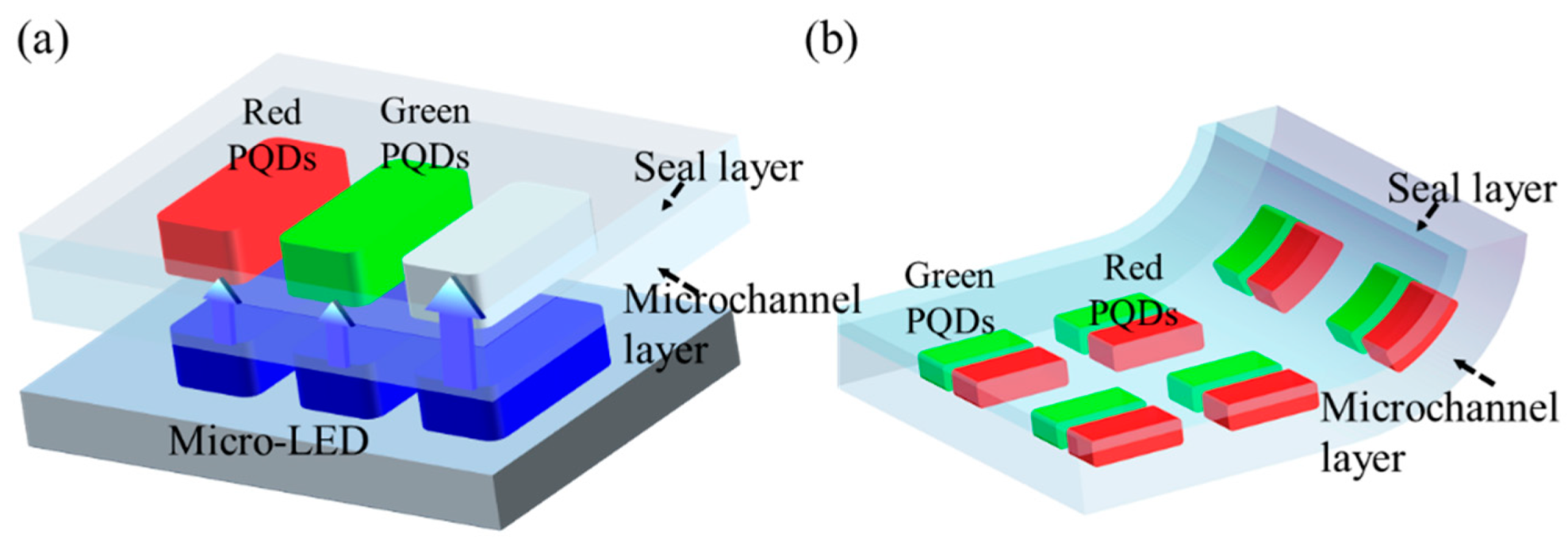
:1. Introduction
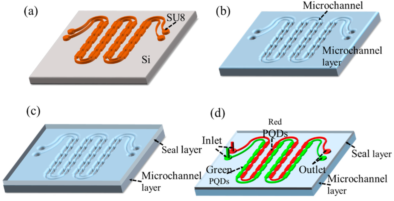
2. Materials and Methods
3. Results and Discussion
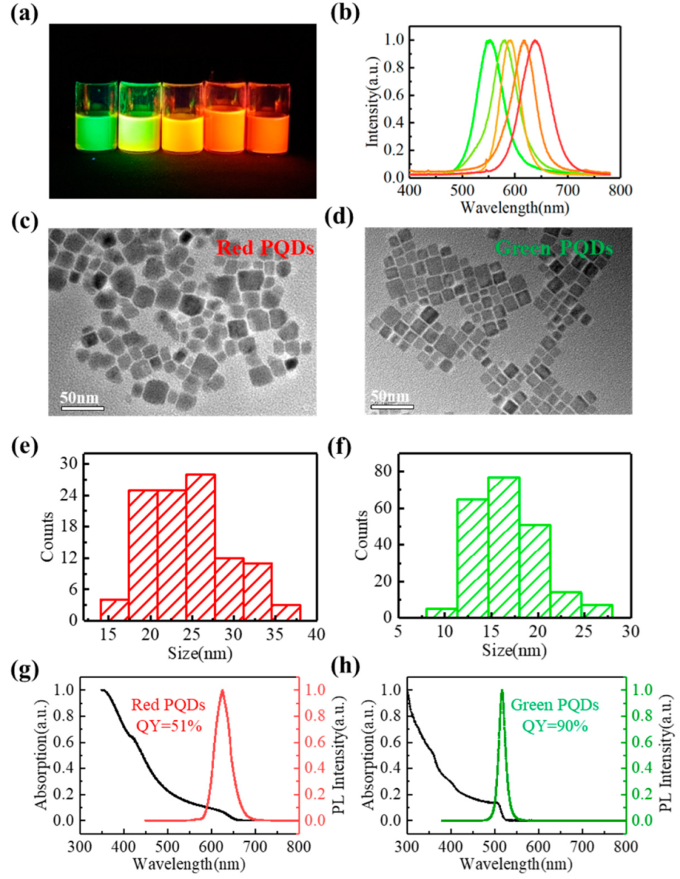
3.1. Preparation and Test of Perovskite Quantum Dots
3.2. Optical Image of FQCL
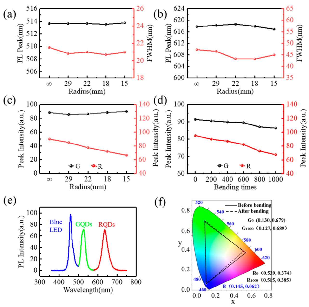
3.3. Bending Test of FQCL Chips
3.4. Temperature Test of FQCL Chips
4. Conclusions
Author Contributions
Funding
Data Availability Statement
Conflicts of Interest
References
- Liu, Z.J.; Chong, W.C.; Wong, K.M.; Lau, K.M. 360 PPI Flip-Chip Mounted Active Matrix Addressable Light Emitting Diode on Silicon (LEDoS) Micro-Displays. J. Disp. Technol. 2013, 9, 678–682. [Google Scholar] [CrossRef]
- Liu, Z.J.; Chong, W.C.; Wong, K.M.; Tam, K.H.; Lau, K.M. A Novel BLU-Free Full-Color LED Projector Using LED on Silicon Micro-Displays. IEEE Photonics Technol. Lett. 2013, 25, 2267–2270. [Google Scholar] [CrossRef]
- Zhang, L.; Ou, F.; Chong, W.C.; Chen, Y.; Li, Q. Wafer-scale monolithic hybrid integration of Si-based IC and III-V epi-layers-A mass manufacturable approach for active matrix micro-LED micro-displays. J. Soc. Inf. Disp. 2018, 26, 137–145. [Google Scholar] [CrossRef]
- Tian, P.; Xie, E.; Gong, Z.; Chen, Z.; Yu, T.; Sun, Y.; Qi, S.; Chen, Y.; Zhang, Y.; Calvez, S.; et al. Flexible vertical structure GaN-based light emitting diodes on an AuSn substrate. In Proceedings of the IEEE Photonic Society 24th Annual Meeting, Arlington, VA, USA, 9–13 October 2011; pp. 551–552. [Google Scholar] [CrossRef]
- Guan, N.; Dai, X.; Messanvi, A.; Zhang, H.; Yan, J.; Gautier, E.; Bougerol, C.; Julien, F.H.; Durand, C.; Eymery, J.; et al. Flexible White Light Emitting Diodes Based on Nitride Nanowires and Nanophosphors. ACS Photonics 2016, 3, 597–603. [Google Scholar] [CrossRef] [Green Version]
- Ren, A.; Wang, H.; Zhang, W.; Wu, J.; Wang, Z.; Penty, R.V.; White, I.H. Emerging light-emitting diodes for next-generation data communications. Nat. Electron. 2021, 4, 559–572. [Google Scholar] [CrossRef]
- Chun, H.; Rajbhandari, S.; Faulkner, G.; Tsonev, D.; Xie, E.; McKendry, J.J.D.; Gu, E.; Dawson, M.D.; O’Brien, D.C.; Haas, H. LED Based Wavelength Division Multiplexed 10 Gb/s Visible Light Communications. J. Light. Technol. 2016, 34, 3047–3052. [Google Scholar] [CrossRef] [Green Version]
- Zhao, L.; Zhu, S.; Wu, C.; Yang, C.; Yu, Z.; Yang, H.; Liu, L. GaN-based LEDs for light communication. Sci. China Ser. G Phys. Mech. Astron. 2016, 59, 107301. [Google Scholar] [CrossRef]
- Pulli, T.; Dönsberg, T.; Poikonen, T.; Manoocheri, F.; Kärhä, P.; Ikonen, E. Advantages of white LED lamps and new detector technology in photometry. Light. Sci. Appl. 2015, 4, e332. [Google Scholar] [CrossRef]
- Poher, V.; Grossman, N.; Kennedy, G.T.; Nikolic, K.; Zhang, H.X.; Gong, Z.; Drakakis, E.M.; Gu, E.; Dawson, M.D.; French, P.M.W.; et al. Micro-LED arrays: A tool for two-dimensional neuron stimulation. J. Phys. D Appl. Phys. 2008, 41, 094014. [Google Scholar] [CrossRef]
- Kim, T.-I.; McCall, J.G.; Jung, Y.H.; Huang, X.; Siuda, E.R.; Li, Y.; Song, J.; Song, Y.M.; Pao, H.A.; Kim, R.-H.; et al. Injectable, Cellular-Scale Optoelectronics with Applications for Wireless Optogenetics. Science 2013, 340, 211–216. [Google Scholar] [CrossRef] [Green Version]
- Huang, Y.; Hsiang, E.-L.; Deng, M.-Y.; Wu, S.-T. Mini-LED, Micro-LED and OLED displays: Present status and future perspectives. Light. Sci. Appl. 2020, 9, 105. [Google Scholar] [CrossRef] [PubMed]
- Wu, Y.; Ma, J.; Su, P.; Zhang, L.; Xia, B. Full-Color Realization of Micro-LED Displays. Nanomaterials 2020, 10, 2482. [Google Scholar] [CrossRef] [PubMed]
- Wang, R.; Nguyen, H.P.T.; Connie, A.T.; Lee, J.; Shih, I.; Mi, Z. Color-tunable, phosphor-free InGaN nanowire light-emitting diode arrays monolithically integrated on silicon. Opt. Express 2014, 22, A1768–A1775. [Google Scholar] [CrossRef] [PubMed]
- Masui, H.; Sonoda, J.; Pfaff, N.; Koslow, I.; Nakamura, S.; Denbaars, S. Quantum-confined Stark effect on photoluminescence and electroluminescence characteristics of InGaN-based light-emitting diodes. J. Phys. D Appl. Phys. 2008, 41, 165105. [Google Scholar] [CrossRef]
- Sekiguchi, H.; Kishino, K.; Kikuchi, A. Ti-mask Selective-Area Growth of GaN by RF-Plasma-Assisted Molecular-Beam Epitaxy for Fabricating Regularly Arranged InGaN/GaN Nanocolumns. Appl. Phys. Express 2008, 1, 124002. [Google Scholar] [CrossRef]
- Peng, D.; Zhang, K.; Chao, V.S.-D.; Mo, W.; Lau, K.M.; Liu, Z. Full-Color Pixelated-Addressable Light Emitting Diode on Transparent Substrate (LEDoTS) Micro-Displays by CoB. J. Disp. Technol. 2016, 12, 742–746. [Google Scholar] [CrossRef]
- Corbett, B.; Loi, R.; Zhou, W.; Liu, D.; Ma, Z. Transfer print techniques for heterogeneous integration of photonic components. Prog. Quantum Electron. 2017, 52, 1–17. [Google Scholar] [CrossRef]
- Cok, R.S.; Meitl, M.; Rotzoll, R.; Melnik, G.; Fecioru, A.; Trindade, A.J.; Raymond, B.; Bonafede, S.; Gomez, D.; Moore, T.; et al. Inorganic light-emitting diode displays using micro-transfer printing. J. Soc. Inf. Disp. 2017, 25, 589–609. [Google Scholar] [CrossRef]
- Liu, Z.; Lin, C.-H.; Hyun, B.-R.; Sher, C.-W.; Lv, Z.; Luo, B.; Jiang, F.; Wu, T.; Ho, C.-H.; Kuo, H.-C.; et al. Micro-light-emitting diodes with quantum dots in display technology. Light. Sci. Appl. 2020, 9, 83. [Google Scholar] [CrossRef]
- Shan, Q.; Wei, C.; Jiang, Y.; Song, J.; Zou, Y.; Xu, L.; Fang, T.; Wang, T.; Dong, Y.; Liu, J.; et al. Perovskite light-emitting/detecting bifunctional fibres for wearable LiFi communication. Light. Sci. Appl. 2020, 9, 163. [Google Scholar] [CrossRef]
- Han, H.-V.; Lin, H.-Y.; Lin, C.-C.; Chong, W.-C.; Li, J.-R.; Chen, K.-J.; Yu, P.; Chen, T.-M.; Chen, H.-M.; Lau, K.M.; et al. Resonant-enhanced full-color emission of quantum-dot-based micro LED display technology. Opt. Express 2015, 23, 32504–32515. [Google Scholar] [CrossRef] [PubMed]
- Lin, H.-Y.; Sher, C.-W.; Hsieh, D.-H.; Chen, X.-Y.; Chen, H.-M.P.; Chen, T.-M.; Lau, K.-M.; Chen, C.-H.; Lin, C.-C.; Kuo, H.-C. Optical cross-talk reduction in a quantum-dot-based full-color micro-light-emitting-diode display by a lithographic-fabricated photoresist mold. Photonics Res. 2017, 5, 411–416. [Google Scholar] [CrossRef]
- Chen, G.-S.; Wei, B.-Y.; Lee, C.-T.; Lee, H.-Y. Monolithic Red/Green/Blue Micro-LEDs With HBR and DBR Structures. IEEE Photonics Technol. Lett. 2017, 30, 262–265. [Google Scholar] [CrossRef]
- Guilhabert, B.; Elfström, D.; Kuehne, A.J.C.; Massoubre, D.; Zhang, H.X.; Jin, S.R.; Mackintosh, A.R.; Gu, E.; Pethrick, R.A.; Dawson, M. Integration by self-aligned writing of nanocrystal/epoxy composites on InGaN micro-pixelated light-emitting diodes. Opt. Express 2008, 16, 18933–18941. [Google Scholar] [CrossRef] [PubMed]
- Li, X.; Kundaliya, D.; Tan, Z.J.; Anc, M.; Fang, N.X. Projection lithography patterned high-resolution quantum dots/thiol-ene photo-polymer pixels for color down conversion. Opt. Express 2019, 27, 30864–30874. [Google Scholar] [CrossRef] [PubMed]
- Bianco, V.; Mandracchia, B.; Marchesano, V.; Pagliarulo, V.; Olivieri, F.; Coppola, S.; Paturzo, M.; Ferraro, P. Endowing a plain fluidic chip with micro-optics: A holographic microscope slide. Light. Sci. Appl. 2017, 6, e17055. [Google Scholar] [CrossRef]
- Whitesides, G.M. The origins and the future of microfluidics. Nature 2006, 442, 368–373. [Google Scholar] [CrossRef]
- Dai, X.; Messanvi, A.; Zhang, H.; Durand, C.; Eymery, J.; Bougerol, C.; Julien, F.H.; Tchernycheva, M. Flexible Light-Emitting Diodes Based on Vertical Nitride Nanowires. Nano Lett. 2015, 15, 6958–6964. [Google Scholar] [CrossRef] [Green Version]
- Tian, P.; McKendry, J.; Gu, E.; Chen, Z.; Sun, Y.; Zhang, G.; Dawson, M.; Liu, R. Fabrication, characterization and applications of flexible vertical InGaN micro-light emitting diode arrays. Opt. Express 2016, 24, 699–707. [Google Scholar] [CrossRef] [Green Version]
- Wang, X.; Bao, Z.; Chang, Y.-C.; Liu, R.-S. Perovskite Quantum Dots for Application in High Color Gamut Backlighting Display of Light-Emitting Diodes. ACS Energy Lett. 2020, 5, 3374–3396. [Google Scholar] [CrossRef]
- Dohnalová, K.; Poddubny, A.N.; Prokofiev, A.A.; De Boer, W.D.; Umesh, C.P.; Paulusse, J.M.; Zuilhof, H.; Gregorkiewicz, T. Surface brightens up Si quantum dots: Direct bandgap-like size-tunable emission. Light. Sci. Appl. 2013, 2, e47. [Google Scholar] [CrossRef]
- Zhu, X.; Bian, L.; Fu, H.; Wang, L.; Zou, B.; Dai, Q.; Zhang, J.; Zhong, H. Broadband perovskite quantum dot spectrometer beyond human visual resolution. Light. Sci. Appl. 2020, 9, 73. [Google Scholar] [CrossRef] [PubMed]
- Castañeda, J.A.; Nagamine, G.; Yassitepe, E.; Bonato, L.G.; Voznyy, O.; Hoogland, S.; Nogueira, A.F.; Sargent, E.H.; Cruz, C.H.B.; Padilha, L.A. Efficient Biexciton Interaction in Perovskite Quantum Dots Under Weak and Strong Confinement. ACS Nano 2016, 10, 8603–8609. [Google Scholar] [CrossRef] [PubMed]
- Su, Y.; Chen, X.; Ji, W.; Zeng, Q.; Ren, Z.; Su, Z.; Liu, L. Highly Controllable and Efficient Synthesis of Mixed-Halide CsPbX3 (X = Cl, Br, I) Perovskite QDs toward the Tunability of Entire Visible Light. ACS Appl. Mater. Interfaces 2017, 9, 33020–33028. [Google Scholar] [CrossRef]
- Wang, H.-C.; Lin, S.-Y.; Tang, A.-C.; Singh, B.P.; Tong, H.-C.; Chen, C.-Y.; Lee, Y.-C.; Tsai, T.-L.; Liu, R. Mesoporous Silica Particles Integrated with All-Inorganic CsPbBr3 Perovskite Quantum-Dot Nanocomposites (MP-PQDs) with High Stability and Wide Color Gamut Used for Backlight Display. Angew. Chem. Int. Ed. 2016, 55, 7924–7929. [Google Scholar] [CrossRef]


Publisher’s Note: MDPI stays neutral with regard to jurisdictional claims in published maps and institutional affiliations. |
© 2022 by the authors. Licensee MDPI, Basel, Switzerland. This article is an open access article distributed under the terms and conditions of the Creative Commons Attribution (CC BY) license (https://creativecommons.org/licenses/by/4.0/).
Share and Cite
Li, P.; Tao, J.; Zhao, Y.; Sun, Y.; Fan, K.; Zhu, L.; Sun, W.; Lv, J.; Qin, Y.; Wang, Q.; et al. Flexible Quantum-Dot Color-Conversion Layer Based on Microfluidics for Full-Color Micro-LEDs. Micromachines 2022, 13, 448. https://doi.org/10.3390/mi13030448
Li P, Tao J, Zhao Y, Sun Y, Fan K, Zhu L, Sun W, Lv J, Qin Y, Wang Q, et al. Flexible Quantum-Dot Color-Conversion Layer Based on Microfluidics for Full-Color Micro-LEDs. Micromachines. 2022; 13(3):448. https://doi.org/10.3390/mi13030448
Chicago/Turabian StyleLi, Panyuan, Jin Tao, Yongzhou Zhao, Yifang Sun, Kaili Fan, Licai Zhu, Wenchao Sun, Jinguang Lv, Yuxin Qin, Qiang Wang, and et al. 2022. "Flexible Quantum-Dot Color-Conversion Layer Based on Microfluidics for Full-Color Micro-LEDs" Micromachines 13, no. 3: 448. https://doi.org/10.3390/mi13030448
APA StyleLi, P., Tao, J., Zhao, Y., Sun, Y., Fan, K., Zhu, L., Sun, W., Lv, J., Qin, Y., Wang, Q., Zeng, Q., Wang, W., Wang, S., & Liang, J. (2022). Flexible Quantum-Dot Color-Conversion Layer Based on Microfluidics for Full-Color Micro-LEDs. Micromachines, 13(3), 448. https://doi.org/10.3390/mi13030448