Abstract
A p-GaN HEMT with an AlGaN cap layer was grown on a low resistance SiC substrate. The AlGaN cap layer had a wide band gap which can effectively suppress hole injection and improve gate reliability. In addition, we selected a 0° angle and low resistance SiC substrate which not only substantially reduced the number of lattice dislocation defects caused by the heterogeneous junction but also greatly reduced the overall cost. The device exhibited a favorable gate voltage swing of 18.5 V (@IGS = 1 mA/mm) and an off-state breakdown voltage of 763 V. The device dynamic characteristics and hole injection behavior were analyzed using a pulse measurement system, and Ron was found to increase and VTH to shift under the gate lag effect.
1. Introduction
GaN power transistors have become key devices in high-power and high-efficiency power conversion systems, mainly because of their material properties, such as a wide band gap, high mobility, and strong electric breakdown field. Various approaches, such as the gate recessed structure [1,2,3], fluorine ion treatment [4], and a p-type GaN cap layer have been reported for giving these devices normally-off operation [5,6,7]. The other advantages of GaN power transistors are their high breakdown voltage, high switching speed, and low on-resistance. Therefore, p-GaN gate normally-off power devices have been considered as key devices in high power and high-frequency applications such as power conversion systems in hybrid or electric vehicles [8]. Normally-off operation is necessary for such applications because the current must be cut off in case of uncontrollable situations, such as short and open modes.
In commercial p-GaN HEMTs, device gates are either ohmic contacts or Schottky contacts. Compared with ohmic gates, such as gate injection transistors, Schottky gates have a lower forward gate leakage current, mainly due to a reverse Schottky diode at the junction of the metal and p-GaN. A Schottky gate p-GaN HEMT also exhibits a time-dependent gate breakdown voltage, but the gate’s operating voltage is limited to 6–7 V. Therefore, many research groups are developing methods to increase this maximum value so that the device can be operated in a wider gate bias range [9]. Under positive bias, the gate breakdown of a p-GaN HEMT can be attributed to the strong electric field concentrated at the metal/p-GaN interface [10]. Different from the time-dependent dielectric breakdown performance of Si and SiC power MOSFETs, the time-dependent gate breakdown behavior of p-GaN HEMTs is usually positively correlated with the temperature coefficient which means that high-energy carriers are accelerated through impact ionization or hot electron bombardment in a strong electric field. Therefore, one of the methods for improving the reliability of a gate is to make structural or process changes at the metal/p-GaN junction. Conversely, many scholars have analyzed the physical mechanism of dynamic resistance change which is mainly due to hot electron injection on the surface and defects in the buffer layer. These defects have numerous forms, such as carrier vacancies, lattice dislocations, and impurities. Additionally, GaN devices are mostly operated under high frequency and power. Thus, the characteristics of the device during high-temperature operation are also critical. Two substrates are employed in p-GaN HEMTs, namely GaN-on-Si and GaN-on-SiC. Compared with a GaN-on-Si HEMT, a GaN-on-SiC HEMT should be a more favorable choice for high-power switching components because of its high thermal conductivity, low resistivity, and high-voltage capability. Another advantage of using a SiC substrate is its lower lattice mismatch of approximately 3% for GaN (that of Si is ~17%). Therefore, a low-resistance and 0°-angle SiC substrate not only has the aforementioned advantages of GaN-on-SiC but also has a lower cost than a high-resistivity SiC substrate. We previously employed an AlGaN cap layer and low-resistivity SiC substrate in a p-GaN HEMT [11,12].
2. Device Structure
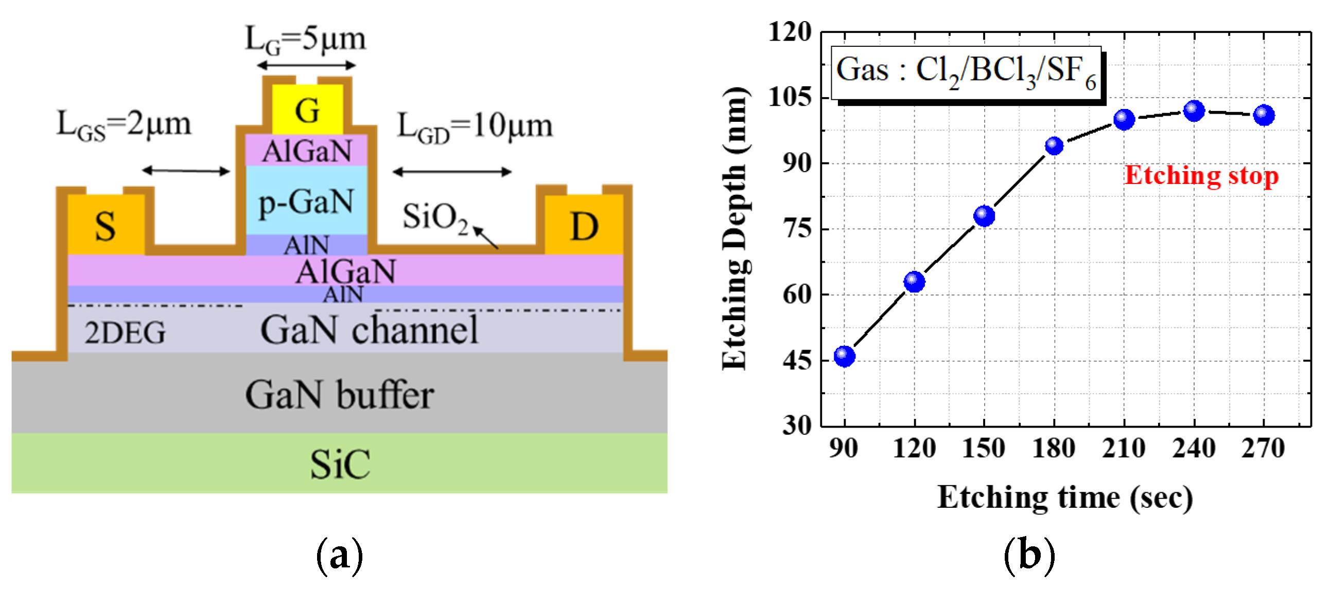
In this study, an AlGaN/p-GaN/AlN/AlGaN/GaN HEMT was grown on a 6-inch low-resistivity SiC substrate through metalorganic chemical vapor deposition. The epitaxial structure is illustrated in Figure 1a. An undoped GaN channel layer with a thickness of 300 nm was grown on an undoped AlGaN/GaN buffer/transition layer with a thickness of 4 μm. Subsequently, an Al0.25Ga0.75N barrier layer with a thickness of 15 nm and a p-type GaN layer with a thickness of 100 nm were grown.

Figure 1.
(a) Cross-sectional schematic of the p-GaN gate HEMT, and (b) the etching stop technique.
Finally, an Al0.2Ga0.8N layer of 10 nm thickness was grown on the p-GaN layer. In the device fabrication, the p-GaN etching of Cl2/BCl3/SF6 was achieved using inductively coupled plasma, and the AlN layer acted as an etching stop layer. The etching stop technique employed was similar to that used in the p-GaN etching process [13,14,15]. The etching rate for p-GaN layer etching was approximately 31.5 nm/min. From 210 to 270 s, the etching rate was reduced to less than 2 nm/min because of generation of the AlF3 layer (etching stop layer). This etching stop technique prevents overetching in the p-GaN removal process, as shown in Figure 1b. Ohmic contacts were prepared through electron beam evaporation, and Ti, Al, Ni, and Au layers (thickness = 25, 120, 25, and 150 nm, respectively) were stacked on the device sequentially. Both devices were then annealed using a rapid thermal annealing system at 875 °C for 30 s in ambient N2. Finally, a Ni/Au (25/120 nm) gate metal stack was deposited and a 100-nm SiO2 passivation layer was applied.
3. Experimental Result and Discussion
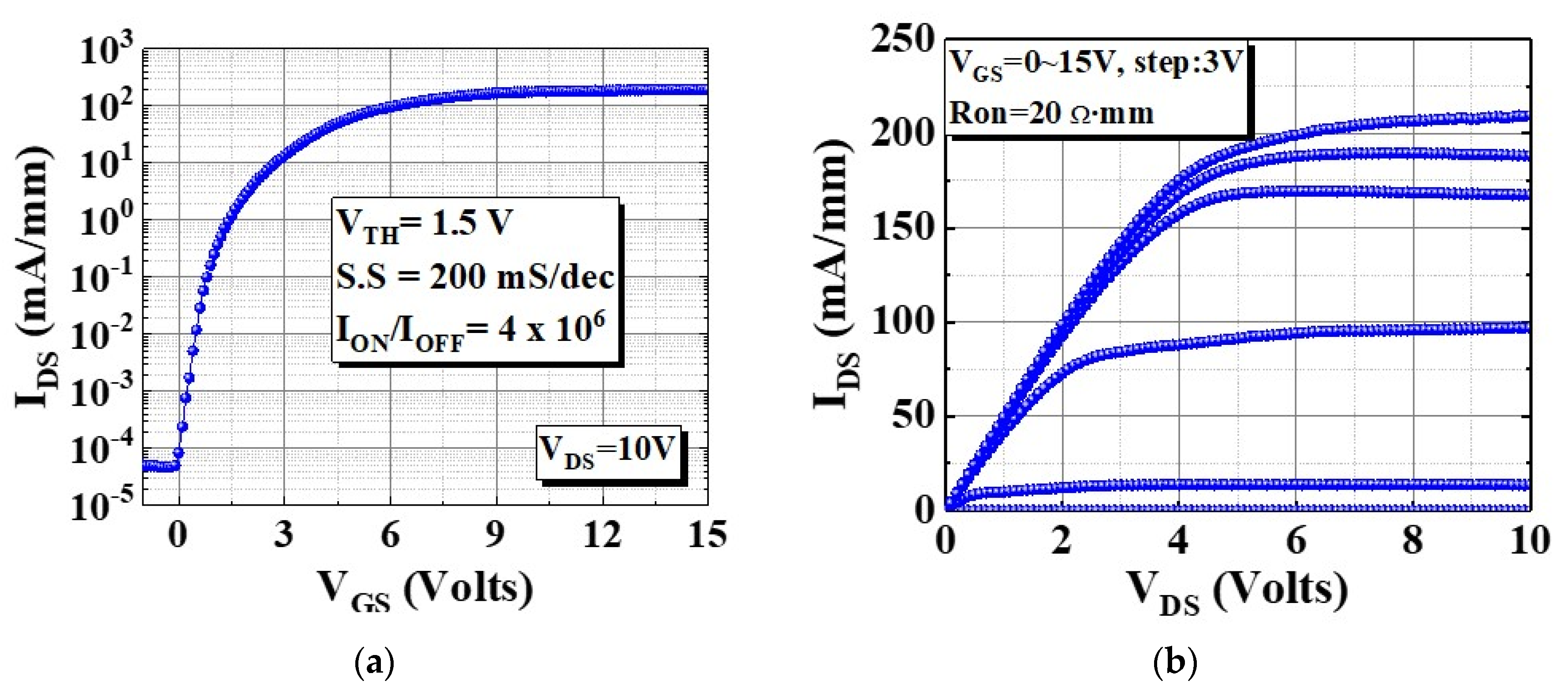
Figure 2a,b reveal the log-scale transfer (IDS–VGS) and output (IDS–VDS) characteristics of the device. As illustrated in Figure 2a, the off-state current was 5 × 10⁻⁵ mA/mm at VGS = 0 V. Additionally, the threshold voltage VTH was 1.5 V which is defined at IDS = 1 mA/mm. The corresponding maximum drain current density IDmax and Ron were 210 mA/mm and 20 Ω mm, respectively.

Figure 2.
Device’s dc characteristics with LGS, LG, LGD, and WG = 2, 5, 10, and 100 μm, respectively: (a) transfer and (b) output characteristics.
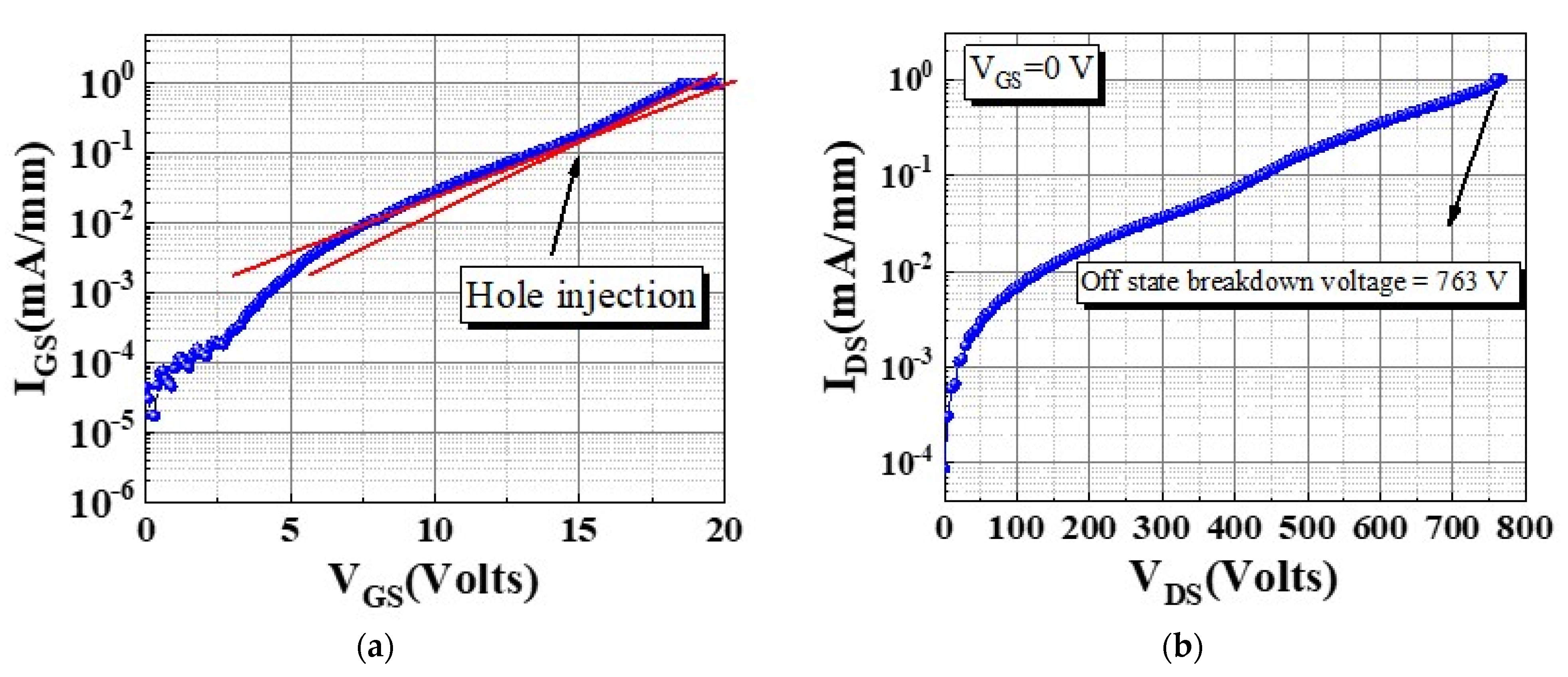
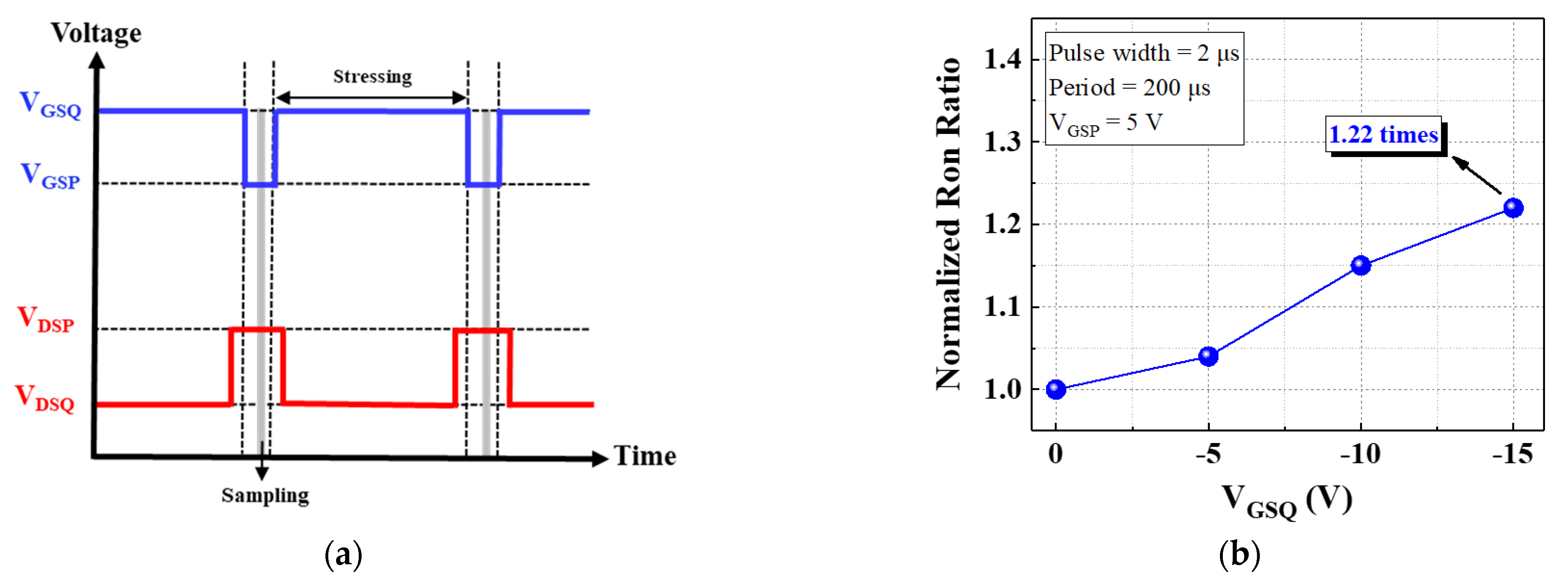
To observe the hole injection effect during gate operation, IGS–VGS measurements were made [Figure 3a]. The device exhibited a large gate operation voltage under forward bias, and the gate turn-on voltage VGS_ON was 18.5 V at IGS = 1 mA/mm. The device exhibited favorable gate behavior because of its higher barrier which effectively suppressed the carrier injection. As revealed by Figure 3b, the device exhibited a high off-state breakdown voltage of 763 V. We used pulse measurement to analyze the hole injection effect and dynamic characteristics of the device under various stress voltages VGSQ and durations. To evaluate the gate lag behavior we employed the AM-241 pulse measurement system [16,17]. The operation condition and gate lag measurement are illustrated in Figure 4a,b, respectively. Two bias conditions had to be considered: pulse voltage (VGSP and VDSP) and quiescent voltage (VGSQ and VDSQ). During the measurement, the pulse voltage switched rapidly to the quiescent voltage with a 2 µs pulse width and 200 µs period, and VGSQ was swept from 0 to −15 V in increments of −5 V. The device exhibited dynamic Ron of 1.22 times at VGSQ = −15 V.
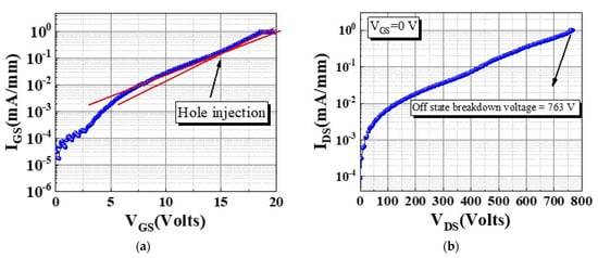
Figure 3.
(a) IGS−VGS characteristic and (b) off−state breakdown voltage measurement of the device.
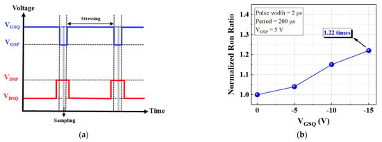
Figure 4.
(a) Condition of pulse measurement and (b) gate lag characteristic.
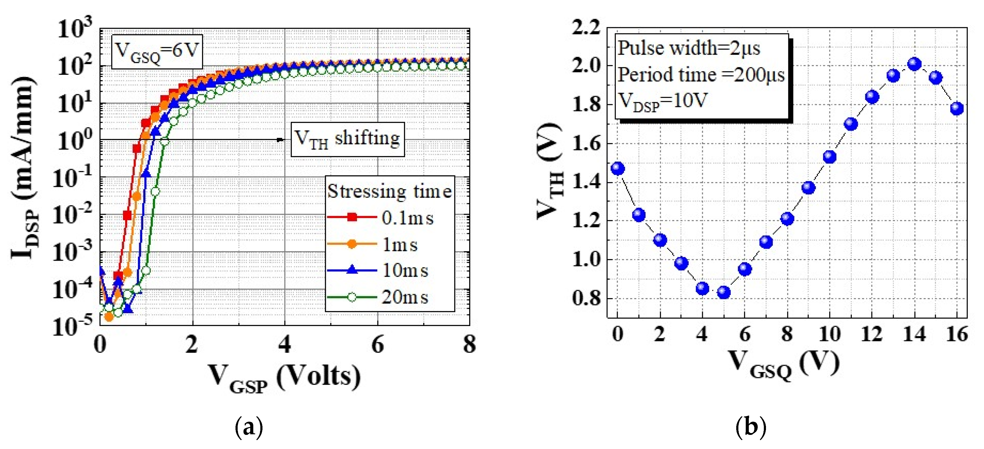
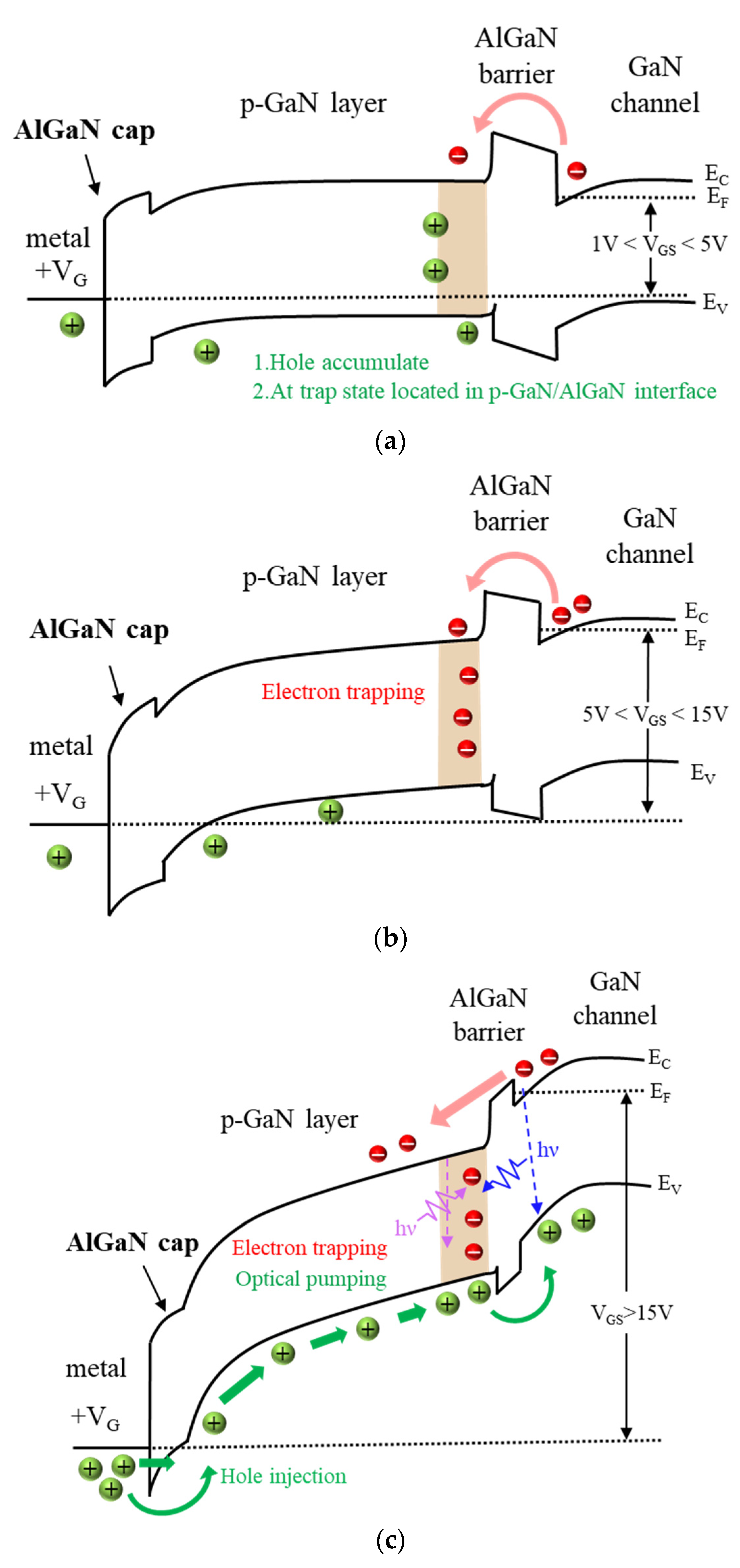
As indicated in Figure 5a, VTH shifted in the positive direction under VGSQ = 6 V when the stress duration was increased from 0.1 ms to 1, 10, and 20 ms. This was caused by an enhanced electron injection from the channel at a higher VGSQ and trapping at the p-GaN/AlN/AlGaN interfaces. Moreover, the VTH shifting could be plotted in the pulse measurement, as presented in Figure 5b. When VGSQ from 1 to 5 V was applied, holes may have accumulated at the p-GaN/AlGaN interface [Figure 6a] or in trap states at the AlGaN/GaN interface, temporarily increasing the density of the two-dimensional electron gas and causing a negative shift in VTH. When VGSQ from 5 to 15 V was applied, VTH shifted in the positive direction. This can be explained by some injected electrons being captured by the electron traps at the p-GaN/AlGaN interface, with the trapped electrons not being able to immediately escape [Figure 6b]. Subsequently, the stress voltage was larger than 15 V, and the hole injection was turned on for injection of the p-GaN/AlGaN interface, leading to recombination of the trapped electrons [Figure 6c]. Thus, the VTH shift was reversed again [18,19,20,21,22].
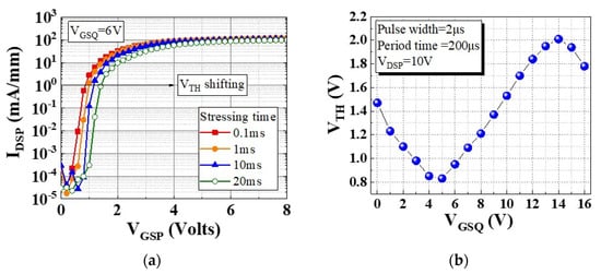
Figure 5.
(a) Dynamic transfer characteristics measured for various stress durations, and (b) VTH shifting for different VGSQ.
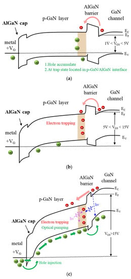
Figure 6.
Schematic of the band diagram gate region of a p-GaN HEMT operating at (a) 1 V < VGS < 5 V, (b) 5 V < VGS < 15 V, and (c) VGS > 15 V.
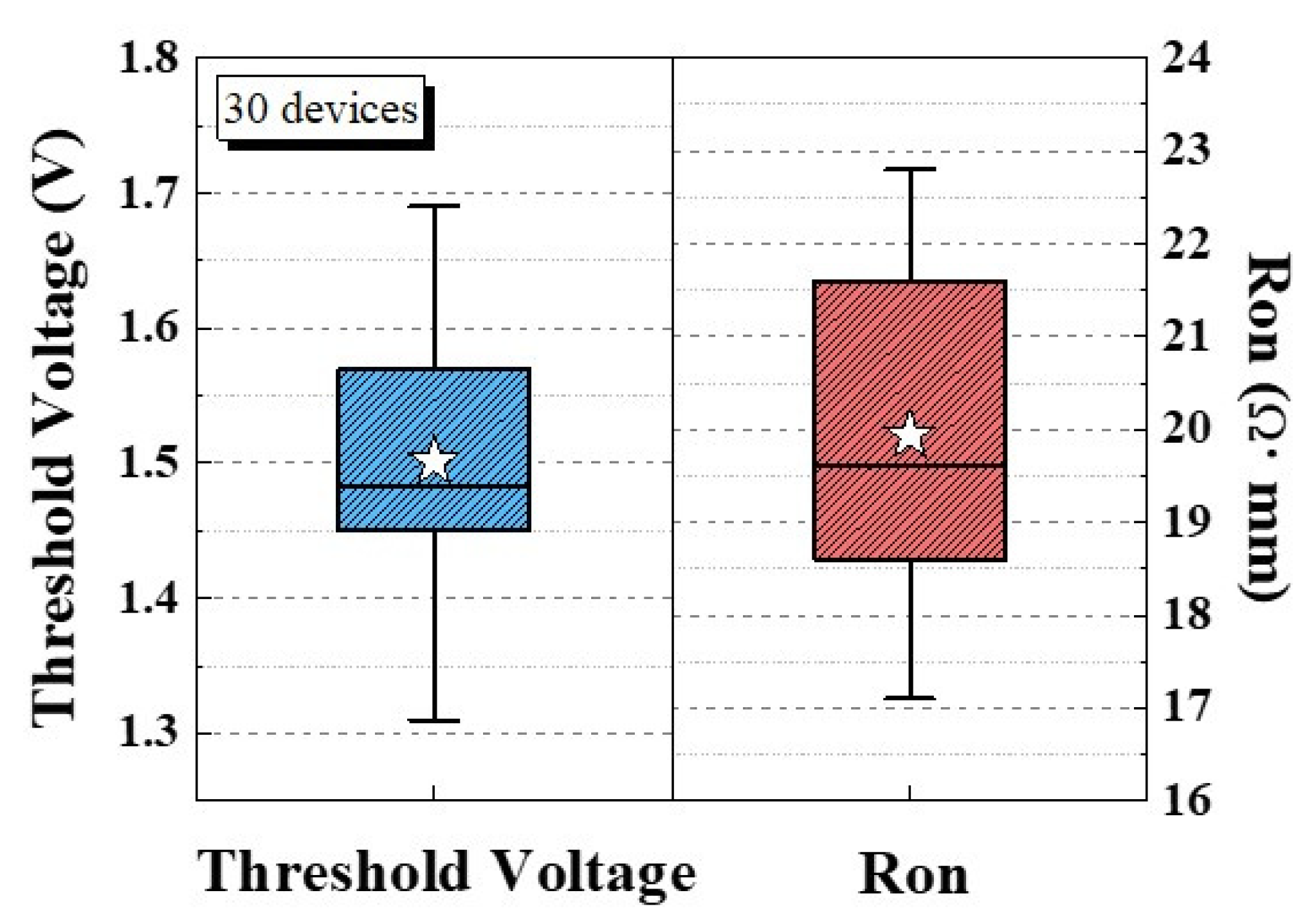
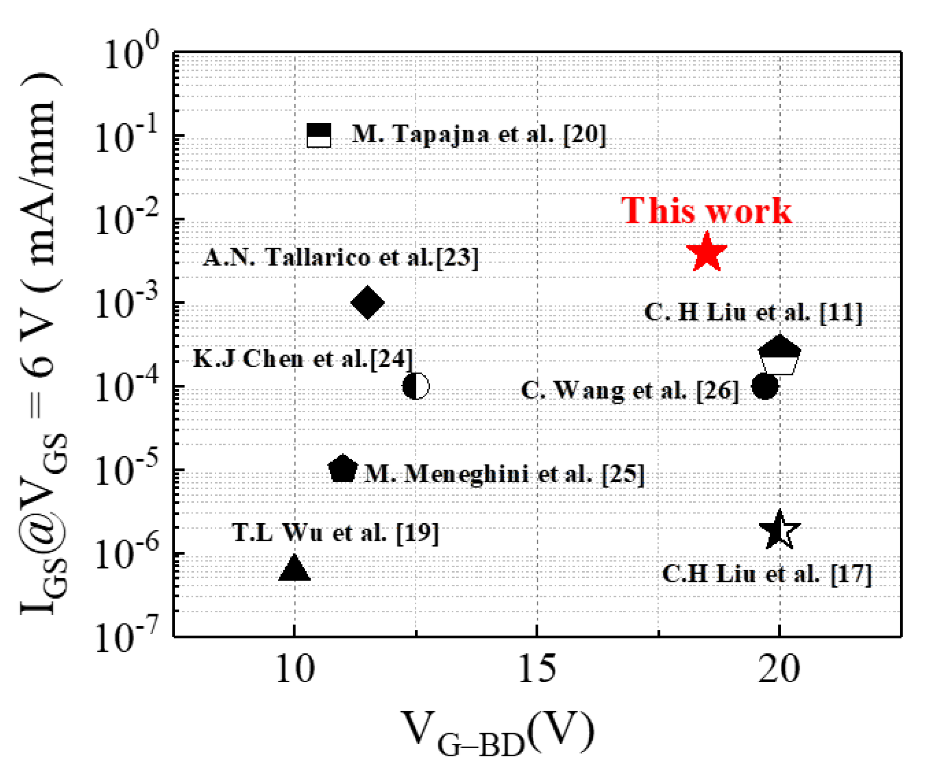
To analyze the thermal characteristics of the device, its IDS–VGS characteristic was measured under 25 °C to 175 °C with a 50 °C step [Figure 7a]. The device exhibited a VTH shift of less than 0.3 V and Ron increased to 1.28× at 175 °C [Figure 7b]. Therefore, the p-GaN HEMT on a SiC substrate has high thermal stability because of its high thermal dissipation ability. Finally, the distributions of VTH and Ron characteristics for 30 devices were measured and are presented in Figure 8. The mean VTH and Ron were 1.5 V and 20 Ω·mm, respectively. Finally, the comparison of gate breakdown voltage and gate leakage current at VGS = 6 V with each group were shown in Figure 9 [11,17,19,20,23,24,25,26].
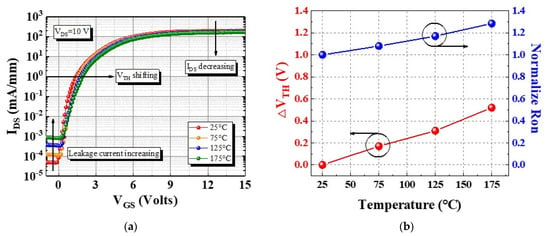
Figure 7.
(a) IDS–VGS characteristics of the device at 25 °C to 175 °C, and (b) variation in VTH and Ron.
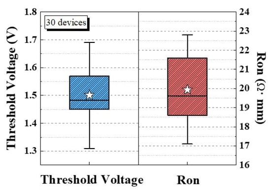
Figure 8.
VTH and Ron distributions for 30 devices.
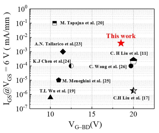
Figure 9.
Comparison with other teams of the VGB−D and IGS−Leakage.
4. Conclusions
In the device developed in this study, an AlGaN cap on the p-GaN layer reduced the hole injection effect and created a large gate operation range. It is hoped that the gate driver of traditional silicon devices can be shared and the operating safety voltage of the gate can be increased simultaneously. In addition, we grew a p-GaN HEMT with an AlGaN cap layer on a low-resistance SiC substrate, thus lowering the lattice defect density at the buffer layer position of the GaN-on-SiC structure. This improved the heat dissipation performance and lowered the cost of device production.
Author Contributions
Conceptualization, H.-C.W.; Data curation, H.-C.W. and C.-H.L.; Formal analysis, C.-H.L. and C.-R.H.; Investigation, C.-H.L. and C.-R.H.; Writing—original draft preparation, C.-H.L.; Supervision, H.-C.C., H.-L.K. and X.L.; Project administration, H.-C.C.; Resources, H.-L.K. and X.L. All authors have read and agreed to the published version of the manuscript.
Funding
This research was funded by the Ministry of Science and Technology (MOST), Taiwan, grant number MOST 110-2622-E-182-006; and the Chang Gung Memorial Hospital, Taiwan, grant number BMRP828.
Conflicts of Interest
The authors declare no conflict of interest.
References
- Lanford, W.B.; Tanaka, T.; Otoki, Y.; Adesida, I. Recessed-gate enhancement-mode GaN HEMT with high threshold voltage. Electron. Lett. 2005, 41, 449–450. [Google Scholar] [CrossRef]
- Oka, T.; Nozawa, T. AlGaN/GaN recessed MIS-gate HFET with high-threshold-voltage normally-off operation for power electronics applications. IEEE Electron Device Lett. 2008, 29, 668–670. [Google Scholar] [CrossRef]
- Zhou, Q.; Liu, L.; Zhang, A.; Chen, B.; Jin, Y.; Shi, Y.; Wang, Z.; Chen, W.; Zhang, B. 7.6 V threshold voltage high-performance normally-off Al2O3/GaN MOSFET achieved by interface charge engineering. IEEE Electron Device Lett. 2016, 37, 165–168. [Google Scholar] [CrossRef]
- Cai, Y.; Zhou, Y.; Chen, K.J.; Lau, K.M. High-performance enhancement-mode AlGaN/GaN HEMTs using fluoride-based plasma treatment. IEEE Electron Device Lett. 2005, 26, 435–437. [Google Scholar] [CrossRef]
- Uemoto, Y.; Hikita, M.; Ueno, H.; Matsuo, H.; Ishida, H.; Yanagihara, M.; Ueda, T.; Tanaka, T.; Ueda, D. Gate Injection transistor (GIT)—A normally-off AlGaN/GaN power transistor using conductivity modulation. IEEE Trans. Electron Devices 2007, 54, 3393–3399. [Google Scholar] [CrossRef]
- Kaneko, S.; Kuroda, M.; Yanagihara, M.; Ikoshi, A.; Okita, H.; Morita, T.; Tanaka, K.; Hikita, M.; Uemoto, Y.; Takahashi, S.; et al. Current-collapse-free operations up to 850 V by GaNGIT utilizing hole injection from drain. In Proceedings of the 2015 IEEE 27th International Symposium on Power Semiconductor Devices & IC’s (ISPSD), Hong Kong, China, 10–14 May 2015; pp. 41–44. [Google Scholar] [CrossRef]
- Marcon, D.; Saripalli, Y.N.; Decoutere, S. 200 mm GaN-on-Si epitaxy and e-mode device technology. In Proceedings of the 2015 IEEE International Electron Devices Meeting (IEDM), Washington, DC, USA, 7–9 December 2015; pp. 16.2.1–16.2.4. [Google Scholar] [CrossRef]
- Wu, Y.; Jacob-Mitos, M.; Moore, M.L.; Heikman, S. A 97.8% Efficient GaN HEMT Boost Converter with 300-W Output Power at 1 MHz. IEEE Electron Device Lett. 2008, 29, 824–826. [Google Scholar] [CrossRef]
- Zhang, L.; Zheng, Z.; Yang, S.; Song, W.; He, J.; Chen, K.J. p-GaN Gate HEMT with Surface Reinforcement for Enhanced Gate Reliability. IEEE Electron Device Lett. 2021, 42, 22–25. [Google Scholar] [CrossRef]
- Tallarico, A.N.; Stoffels, S.; Posthuma, N.; Decoutere, S.; Sangiorgi, E.; Fiegna, C. Threshold Voltage Instability in GaN HEMTs with p-Type Gate: Mg Doping Compensation. IEEE Electron Device Lett. 2019, 40, 4. [Google Scholar] [CrossRef]
- Liu, C.-H.; Chiu, H.-C.; Wang, H.-C.; Kao, H.-L.; Huang, C.-R. Improved Gate Reliability Normally-Off p-GaN/AlN/AlGaN/GaN HEMT with AlGaN Cap-Layer. IEEE Electron Device Lett. 2021, 42, 10. [Google Scholar] [CrossRef]
- Huang, Y.-C.; Chiu, H.-C.; Kao, H.-L.; Wang, H.-C.; Liu, C.-H.; Huang, C.-R.; Chen, S.-W. High Thermal Dissipation of Normally off p-GaN Gate AlGaN/GaN HEMTs on 6-Inch N-Doped Low-Resistivity SiC Substrate. Micromachines 2021, 12, 509. [Google Scholar] [CrossRef]
- Buttari, D.; Chini, A.; Chakraborty, A.; Mccarthy, L.; Xing, H.; Palacios, T.; Shen, L.; Keller, S.; Mishra, U.K. Selective dry etching of GaN over AlGaN in BCl3/SF6 mixtures. High Perform. Devices 2004, 14, 756–761. [Google Scholar] [CrossRef]
- Chiu, H.C.; Chang, Y.S.; Li, B.H.; Wang, H.C.; Kao, H.L.; Chien, F.T.; Hu, C.W.; Xuan, R. High Uniformity Normally-OFF p-GaN Gate HEMT Using Self-Terminated Digital Etching Technique. IEEE Trans. Electron Devices 2018, 65, 4820–4825. [Google Scholar] [CrossRef]
- Zhong, Y. Self-terminated etching of GaN with a high selectivity over AlGaN under inductively coupled Cl2/N2/O2 plasma with a low-energy ion bombardment. Appl. Surf. Sci. 2018, 420, 817–824. [Google Scholar] [CrossRef]
- Liu, C.-H.; Chiu, H.-C.; Huang, C.-R.; Chang, K.-J.; Chen, C.-T.; Hsueh, K.-P. Low Gate Lag Normally-Off p-GaN/AlGaN/GaN High Electron Mobility Transistor with Zirconium Gate Metal. Crystals 2020, 10, 25. [Google Scholar] [CrossRef] [Green Version]
- Chiu, H.-C.; Liu, C.-H.; Huang, C.-R.; Chiu, C.-C.; Wang, H.-C.; Kao, H.-L.; Lin, S.-Y.; Chien, F.-T. Normally-Off p-GaN Gated AlGaN/GaN MIS-HEMTs with ALD-Grown Al2O3/AlN Composite Gate Insulator. Membranes 2021, 11, 727. [Google Scholar] [CrossRef]
- Meneghini, M. Technology and Reliability of Normally-Off GaN HEMTs with p-Type Gate. Energies 2017, 10, 153. [Google Scholar] [CrossRef] [Green Version]
- Wu, T.L.; Marcon, D.; You, S.; Posthuma, N.; Bakeroot, B.; Stoffels, S.; Van Hove, M.; Groeseneken, G.; Decoutere, S. Forward bias gate breakdown mechanism in enhancement-mode p-GaN gate AlGaN/GaN high-electron mobility transistors. IEEE Electron Device Lett. 2015, 36, 1001–1003. [Google Scholar] [CrossRef]
- Tapajna, M.; Hilt, O.; Bahat-Treidel, E.; Würfl, J.; Kuzmík, J. Gate reliability investigation in normally-off p-type-GaN Cap/AlGaN/GaN HEMTs under forward bias stress. IEEE Electron Device Lett. 2016, 37, 385–388. [Google Scholar] [CrossRef]
- Tang, X.; Li, B.; Moghadam, H.A.; Tanner, P.; Han, J.; Dimitrijev, S. Mechanism of threshold voltage shift in p-GaN gate AlGaN/GaN transistors. IEEE Electron Device Lett. 2018, 39, 1145–1148. [Google Scholar]
- Shi, Y.; Zhou, Q.; Cheng, Q.; Wei, P.; Zhu, L.; Wei, D.; Zhang, A.; Chen, W.; Zhang, B. Carrier Transport Mechanisms Underlying the Bidirectional VTH Shift in p-GaN Gate HEMTs under forward Gate Stress. IEEE Trans. Electron Devices 2019, 66, 2. [Google Scholar] [CrossRef]
- Stoffels, S. Perimeter driven transport in the p-GaN gate as a limiting factor for gate reliability. In Proceedings of the 2019 IEEE International Reliability Physics Symposium (IRPS), Monterey, CA, USA, 31 March–4 April 2019. [Google Scholar]
- He, J.; Chen, K. Frequency and temperature-dependent gate reliability of Schottky-type p-GaN gate HEMTs. IEEE Trans. Electron Devices 2019, 66, 3453–3458. [Google Scholar] [CrossRef]
- Meneghini, M. Gate conduction mechanisms and lifetime modeling of p-Gate AlGaN/GaN high-electron-mobility transistors. IEEE Trans. Electron Devices 2018, 65, 5365–5372. [Google Scholar]
- Wang, C.; Hua, M.; Chen, J.; Yang, S.; Zheng, Z.; Wei, J.; Zhang, L.; Chen, K.J. E-mode p-n junction/AlGaN/GaN (PNJ) HEMTs. IEEE Electron Device Lett. 2020, 41, 545–548. [Google Scholar] [CrossRef]
Publisher’s Note: MDPI stays neutral with regard to jurisdictional claims in published maps and institutional affiliations. |
© 2022 by the authors. Licensee MDPI, Basel, Switzerland. This article is an open access article distributed under the terms and conditions of the Creative Commons Attribution (CC BY) license (https://creativecommons.org/licenses/by/4.0/).

