
A Magnetic Metal Hard Mask on Silicon Substrate for Direct Patterning Ultra-High-Resolution OLED Displays

Abstract
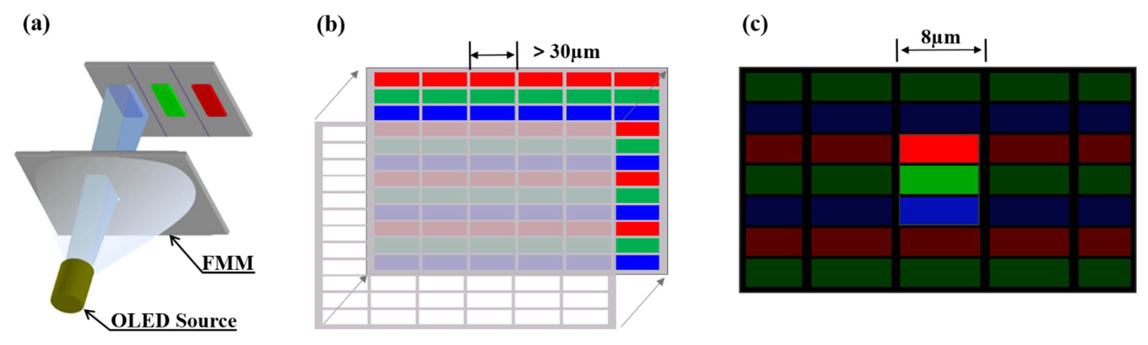
:1. Introduction
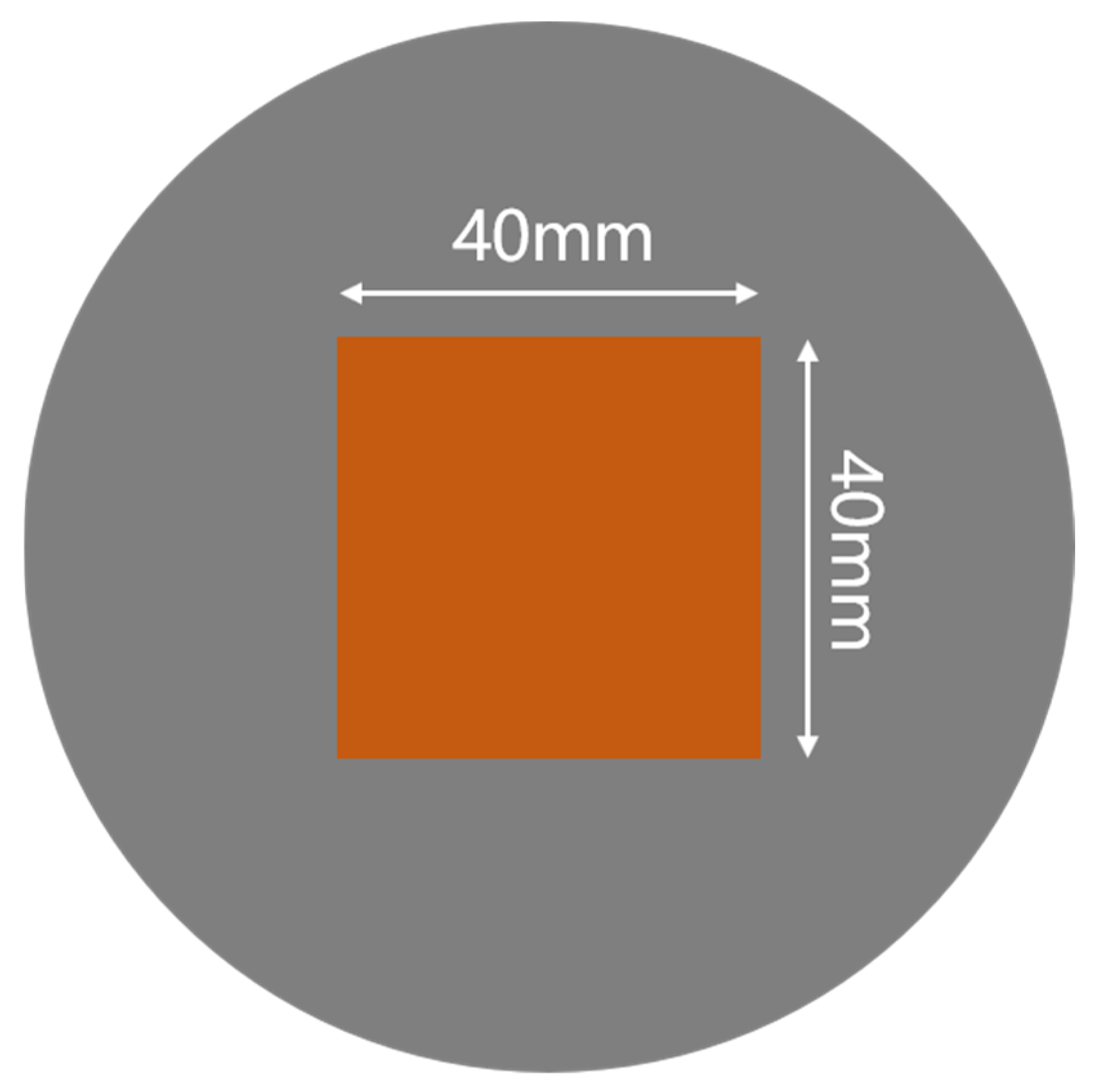
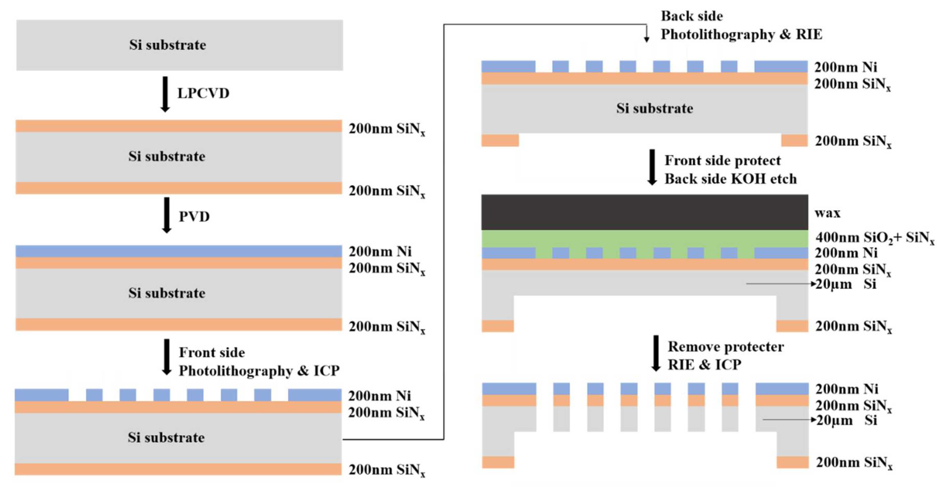
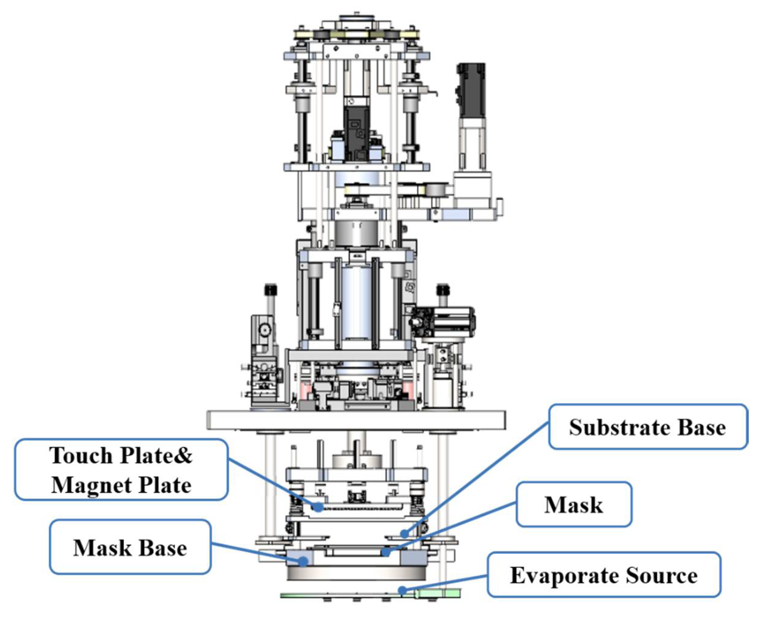
2. Materials and Methods
3. Results and Discussion
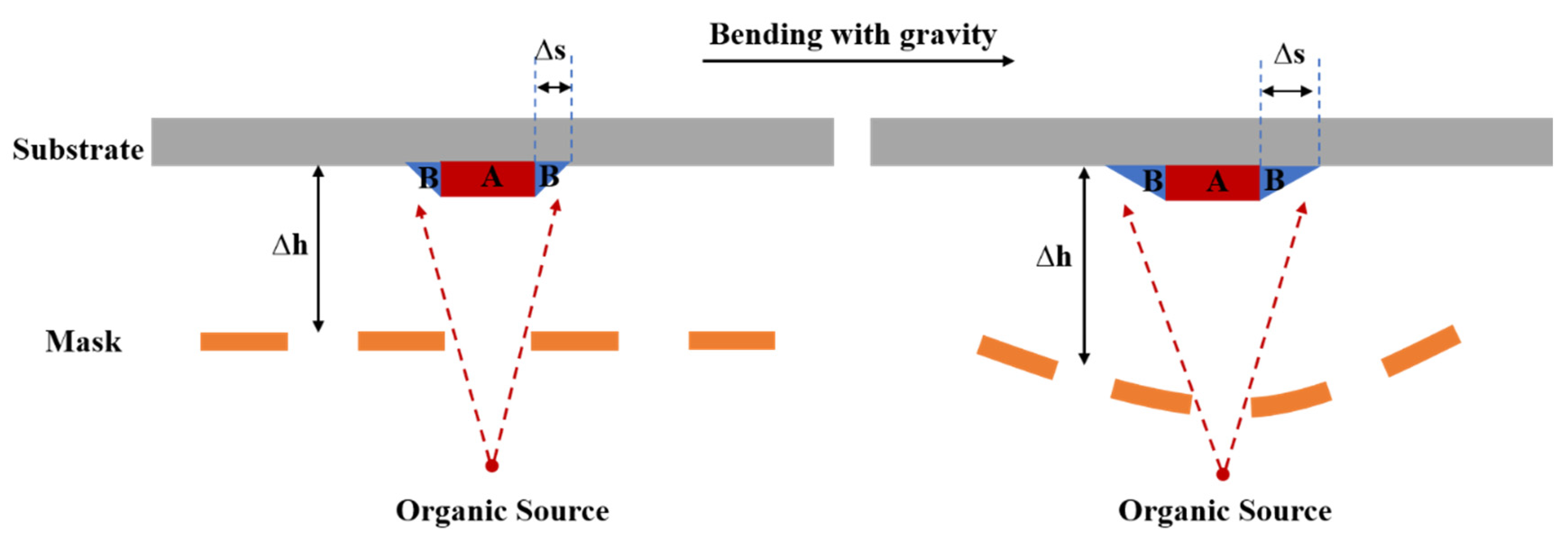
3.1. Measures to Improve PPI
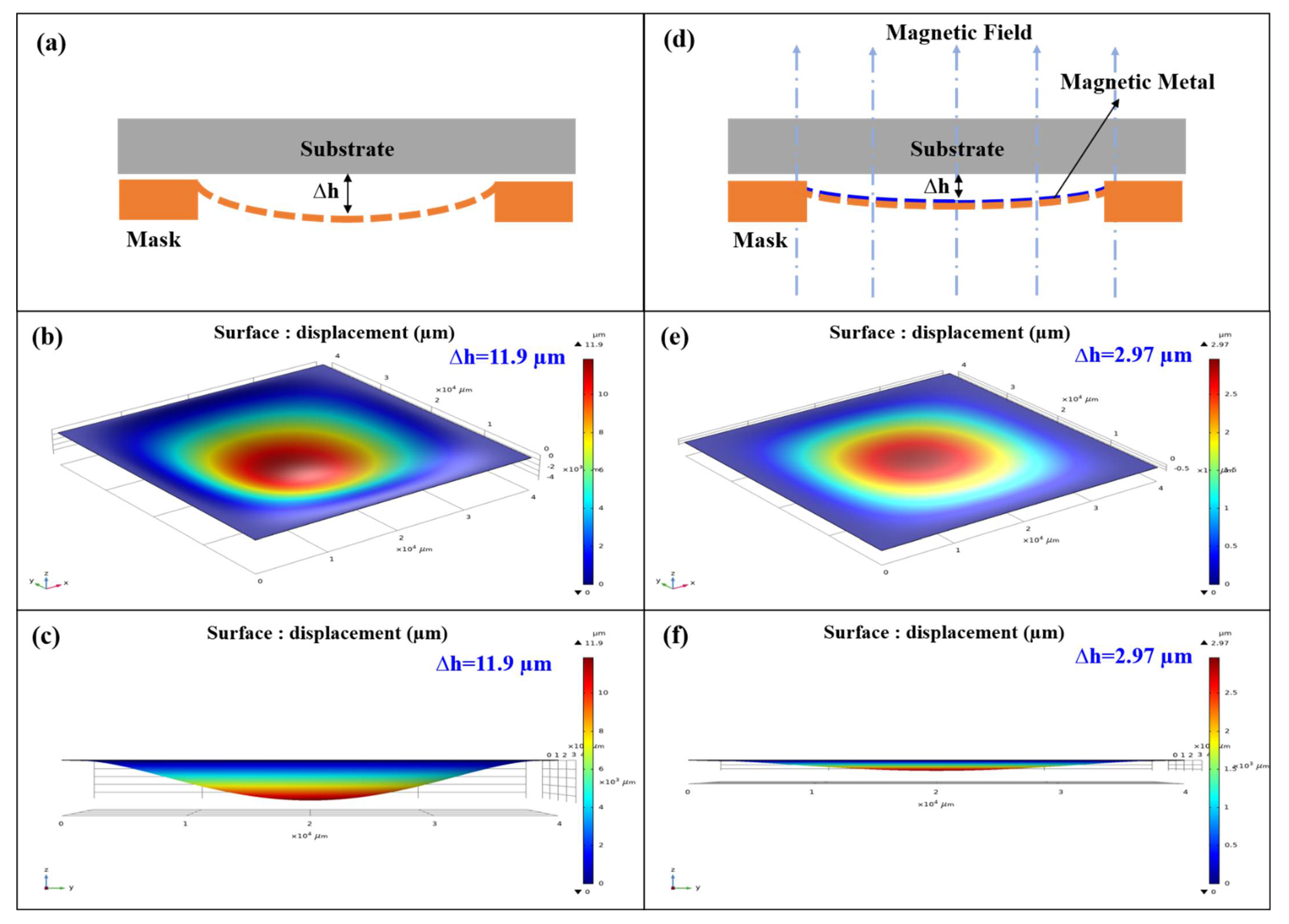
3.2. Measures to Improve Uniformity
4. Conclusions
Author Contributions
Funding
Data Availability Statement
Acknowledgments
Conflicts of Interest
References
- Vieri, C.; Lee, G.; Balram, N. An 18 megapixel 4.3’ 1443 ppi 120 Hz OLED display for wide field of view high acuity head mounted displays. J. Soc. Inf. Disp. 2018, 26, 314–324. [Google Scholar] [CrossRef]
- Korea IT News. Available online: https://english.etnews.com/20210817200001 (accessed on 17 August 2021).
- Ghosh, A.; Donoghue, E.P.; Khayrullin, I. Directly Patterened 2645 PPI Full Color OLED Microdisplay for Head Mounted Wearables. SID Symp. Dig. Tech. Pap. 2016, 47, 837–840. [Google Scholar] [CrossRef]
- Hebner, T.R.; Wu, C.C.; Marcy, D. Ink-jet printing of doped polymers for organic light emitting devices. Appl. Phys. Lett. 1998, 72, 519. [Google Scholar] [CrossRef] [Green Version]
- Shimoda, T.; Morii, K.; Seki, S. Inkjet Printing of Light-Emitting Polymer Displays. MRS Bull. 2003, 28, 821–827. [Google Scholar] [CrossRef]
- Carter, J.; Lyon, P.; Creighton, C. Developing a Scalable and Adaptable Ink Jet Printing Process for OLED Displays. SID Symp. Dig. Tech. Pap. 2012, 26, 523–525. [Google Scholar] [CrossRef]
- Lee, D.; Chung, J.K.; Rhee, J.S. Ink Jet Printed Full Color Polymer LED Displays. SID Symp. Dig. Tech. Pap. 2012, 36, 527–529. [Google Scholar] [CrossRef]
- Lee, S.T.; Chin, B.D.; Kim, M.H. A Novel Patterning Method for Full-Color Organic Light-Emitting Devices: Laser Induced Thermal Imaging (LITI). SID Symp. Dig. Tech. Pap. 2004, 35, 1008–1011. [Google Scholar] [CrossRef]
- Lee, S.T.; Suh, M.C.; Kang, T.M. LITI (Laser Induced Thermal Imaging) Technology for High-Resolution and Large-Sized AMOLED. SID Symp. Dig. Tech. Pap. 2007, 38, 1588–1591. [Google Scholar] [CrossRef]
- Boroson, M.; Tutt, L.; Nguyen, K. Non-Contact OLED Color Patterning by Radiation-Induced Sublimation Transfer (RIST). SID Symp. Dig. Tech. Pap. 2005, 36, 972–975. [Google Scholar] [CrossRef]
- Hirano, T.; Matsuo, K.; Kohinata, K. Novel Laser Transfer Technology for Manufacturing Large-Sized OLED Displays. SID Symp. Dig. Tech. Pap. 2012, 38, 1592–1595. [Google Scholar] [CrossRef]
- Jin, H.; Sturm, J.C. Super-high-resolution transfer printing for full-color OLED display patterning. J. Soc. Inf. Disp. 2010, 18, 141–145. [Google Scholar] [CrossRef] [Green Version]
- Jiang, Y.; Tam, B.; Dong, S. 2-inch, 2,000-ppi Silicon Nitride Mask for Patterning Ultra-High-Resolution OLED Displays. SID Symp. Dig. Tech. Pap. 2020, 51, 909–912. [Google Scholar] [CrossRef]

Publisher’s Note: MDPI stays neutral with regard to jurisdictional claims in published maps and institutional affiliations. |
© 2022 by the authors. Licensee MDPI, Basel, Switzerland. This article is an open access article distributed under the terms and conditions of the Creative Commons Attribution (CC BY) license (https://creativecommons.org/licenses/by/4.0/).
Share and Cite
Chen, L.; Wang, X.; Wei, Y.; Zhou, C. A Magnetic Metal Hard Mask on Silicon Substrate for Direct Patterning Ultra-High-Resolution OLED Displays. Micromachines 2022, 13, 997. https://doi.org/10.3390/mi13070997
Chen L, Wang X, Wei Y, Zhou C. A Magnetic Metal Hard Mask on Silicon Substrate for Direct Patterning Ultra-High-Resolution OLED Displays. Micromachines. 2022; 13(7):997. https://doi.org/10.3390/mi13070997
Chicago/Turabian StyleChen, Lin, Xiuxia Wang, Yu Wei, and Chenggang Zhou. 2022. "A Magnetic Metal Hard Mask on Silicon Substrate for Direct Patterning Ultra-High-Resolution OLED Displays" Micromachines 13, no. 7: 997. https://doi.org/10.3390/mi13070997
APA StyleChen, L., Wang, X., Wei, Y., & Zhou, C. (2022). A Magnetic Metal Hard Mask on Silicon Substrate for Direct Patterning Ultra-High-Resolution OLED Displays. Micromachines, 13(7), 997. https://doi.org/10.3390/mi13070997