Abstract
A normally-off β-Ga2O3 metal-oxide-semiconductor field-effect transistor (MOSFET) is proposed using a technology computer-aided design (TCAD) device simulation, which employs an epitaxial drift layer grown on an n-type low-doped body layer. The low-doped body layer under the MOS gate enabled normally-off operation, whereas the epitaxial drift layer determined the on-resistance and breakdown characteristics. The effects of the doping concentration of each layer and thickness of the drift channel layer on the device characteristics were investigated to design a device with a breakdown voltage of 1 kV. A threshold voltage of 1.5 V and a breakdown voltage of 1 kV were achieved by an n-type body layer with a doping concentration of 1 × 1015 cm−3 and an n-type drift layer with a doping concentration of 3 × 1017 cm−3, a thickness of 150 nm, and a gate-to-drain distance of 9.5 μm; resulting in an on-resistance of 25 mΩ·cm2.
1. Introduction
Wide bandgap (WBG) semiconductors, such as GaN, SiC, and Ga2O3, have been intensively studied to overcome the limitations of Si technology [1,2,3] for the development of next-generation power switching devices. Ga2O3 has a wider energy bandgap (4.5–4.9 eV) than GaN and SiC, with a significantly higher critical electric field of approximately 6–8 MV/cm [2,3,4,5]. Among the various polymorphs, monoclinic β-Ga2O3 is the most stable polymorph [6,7,8,9,10]. Furthermore, Baliga’s figure of merit (BFOM) of β-Ga2O3 is significantly higher than those of GaN and SiC, making it a promising material for high-power switching applications [10]. However, the absence of p-type doping technology for β-Ga2O3 is disadvantageous for the implementation of power switching devices [11,12,13,14,15,16,17]. Although several studies have reported the normally-off operation of β-Ga2O3 field-effect transistors (FET), the experimental results are still far off from the theoretical limits of the material [15,16,17,18].
Chabak et al., demonstrated enhancement-mode FETs using a wrap-gate fin structure in 2016 [15] and a gate recess process in 2018 [16]. In 2017, Wong et al., reported that the utilization of an unintentionally doped β-Ga2O3 channel in MOSFET was able to completely deplete the channel electrons at a gate voltage (VGS) of 0 V, resulting in a positive threshold voltage [19]. In 2019, Singh et al., proposed a T-shaped recessed gate β-Ga2O3 MOSFET to achieve a normally-off operation [16]. The T-shaped recessed gate depleted the channel at a gate bias of 0 V, where the gate oxide (Al2O3) thickness was 20 nm, gate recess depth was 250 nm, and thickness of the active channel under the recess region was 30 nm [17]. The maximum drain current was 40 mA/mm at VGS = +8 V due to the limited channel thickness required to achieve a positive threshold voltage [17].
In this study, we propose a recessed β-Ga2O3 MOSFET with an epitaxial drift layer on top of a low-doped body layer to overcome the trade-off relationship between the threshold voltage and on-current density. The proposed structure does not require precise control of recess depth. Moreover, the threshold voltage could be independently controlled by the drift layer. The output and transfer characteristics of the proposed device were validated using Silvaco ATLAS technology computer-aided design (TCAD) simulation. After investigating the effects of doping concentration on the body layer and additional design parameters of the drift layer, a normally-off MOSFET structure was designed to achieve a breakdown voltage of 1 kV.
2. Simulation and Device Structure
Two-dimensional (2D) device simulations were performed in a Silvaco ATLAS TCAD environment using several physical models, including a drift-diffusion transport model, Fermi–Dirac statistics, concentration and temperature-dependent analytical mobility model, Shockley–Read–Hall recombination model, and an impact ionization model [20,21,22,23,24,25,26]. The material and physical model parameters used in the TCAD simulations are presented in Table 1. Although the simulation process could have been further optimized by employing more comprehensive models [27], the classical models provided by TCAD are sufficient to validate the proposed concept.

Table 1.
Material and physical model parameters used for TCAD simulations [20,21,22,23,24,25,26,28,29].
2.1. Mobility Model
The mobility model used in the simulation included concentration and temperature-dependent relationships based on an analytical function of Caughey–Thomas’ work [25], which is given by:
where α, β, γ, and δ are material-dependent coefficients [20], ND is the impurity concentration, and TL is the temperature in Kelvins. Using the experimental data [28,29], these parameters were determined to be α = 0, β = 0, γ = 0, δ = 0.8, Nref = 1.0 × 1018 cm−3, and TL = 300 K.
2.2. Impact Ionization Model
Selberherr’s model, which is a modification of Chynoweth’s law, has been widely used to predict the breakdown characteristics of wide-bandgap semiconductors [20,21]. The impact ionization coefficient (αn) is given by
where AN and BN are the material coefficients and E is the electric field. In this study, AN = 2.16 × 106 cm−1 and BN = 1.77 × 10⁷ V/cm were used while considering the crystal direction of β-Ga2O3 in the [010] direction and a critical electric field of approximately 5 MV/cm [11,20,21].
2.3. Shockley–Read–Hall Recombination
In our simulations, the recombination rate was obtained using the Shockley–Read–Hall recombination model [26]:
where n, p, and nie are the electron, hole, and intrinsic carrier concentrations, respectively, and k and TL are the Boltzmann constant and lattice temperature, respectively. Etrap is the difference between the trap energy level and the intrinsic Fermi level, and τn0 and τp0 are the electron and hole lifetimes, respectively, which are used as 1.2 × 10⁻⁸ s.
2.4. Device Structure
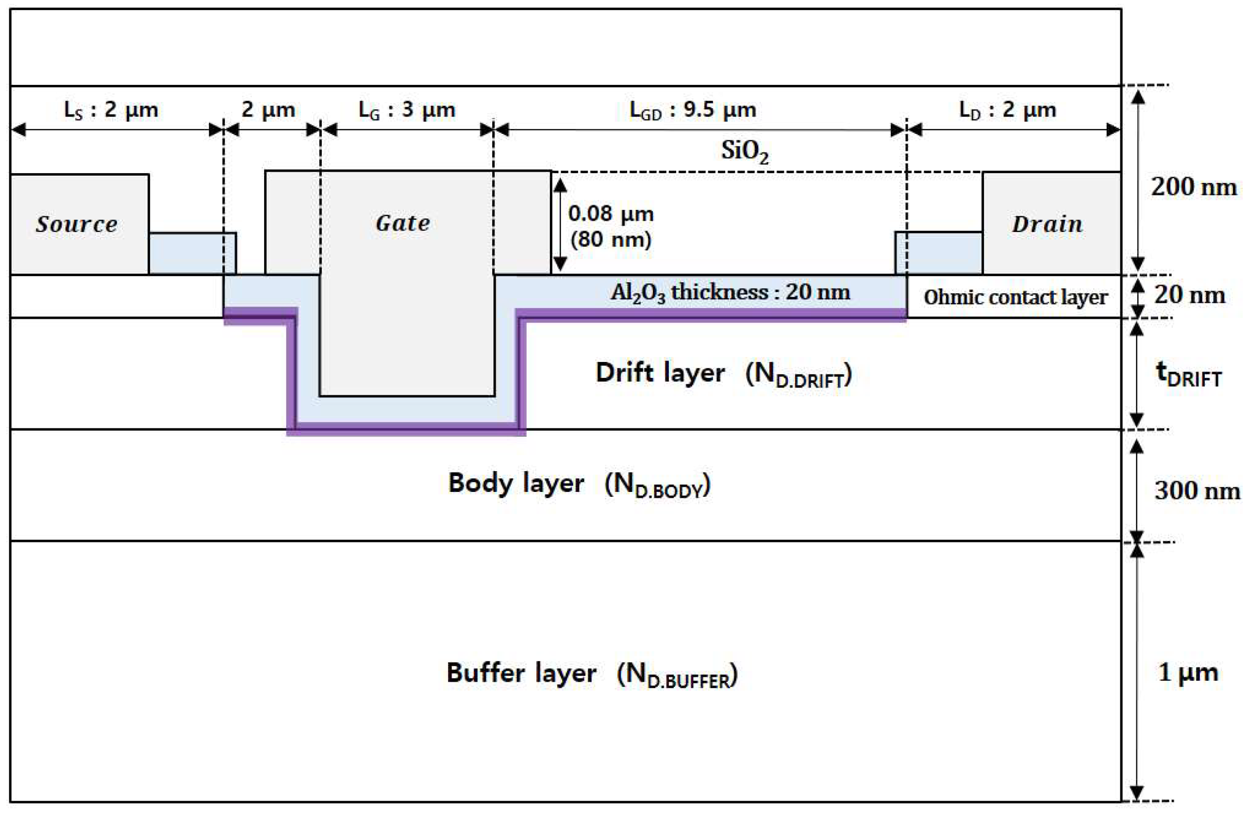
Figure 1 shows a cross-sectional schematic of the β-Ga2O3 MOSFET proposed in this study. The epitaxial structure consisted of a 20 nm thick ohmic contact layer with an n-type doping concentration of 1 × 1020 cm−3, an n-type drift layer, a 300 nm thick low-doped n-type body layer, and a 1 μm thick buffer layer with an n-type doping concentration of 1 × 1012 cm−3. In this study, a highly doped ohmic contact layer was employed instead of an ion-implantation process. The structural variables investigated in this study were the thickness (tDRIFT) and doping concentration (ND.DRIFT) of the drift layer and the doping concentration (ND.BODY) of the body layer. A highly doped ohmic contact layer is etched between the source and drain contacts. The gate region was etched down to the body layer to achieve normally-off characteristics. A 20 nm-thick gate oxide (Al2O3) layer was used, and its interface charges were considered during the simulation.
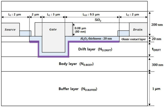
Figure 1.
Cross-sectional schematic of recessed β-Ga2O3 MOSFET with a dual epitaxial structure.
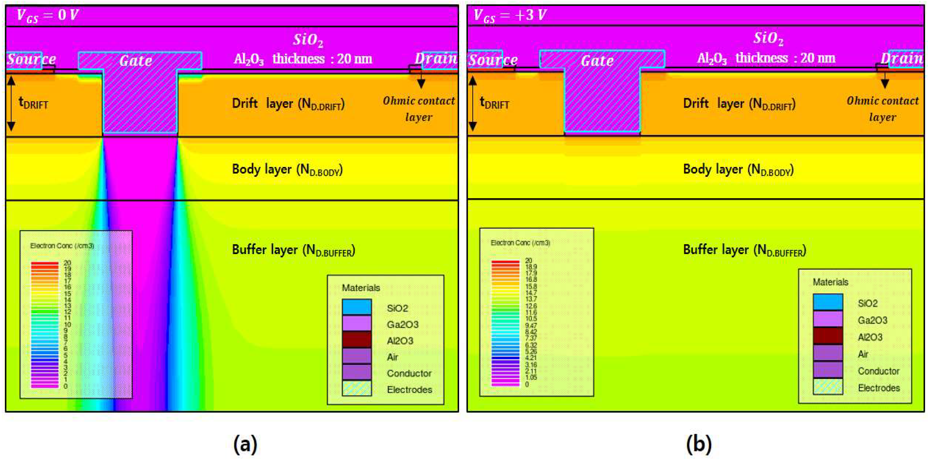
Figure 2a,b show the electron density distributions at VGS = 0 V and +3 V, respectively, which were simulated using the variables ND.DRIFT = 3 × 1017 cm−3, tDRIFT = 300 nm, and ND.BODY = 1 × 1015 cm−3. For VGS = 0 V, the electrons in the region under the gate were completely depleted, which blocked the flow of current, confirming the normally-off characteristics. For VGS = +3 V, the depletion region under the gate disappeared, creating an electron accumulation channel layer and allowing for current flow.
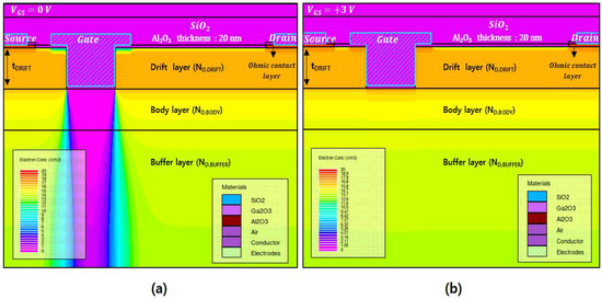
Figure 2.
Electron density distributions simulated with a gate voltage of (a) VGS = 0 V and (b) VGS = +3 V.
3. Results and Discussions
3.1. Effects of Al2O3/β-Ga2O3 Interface Charge
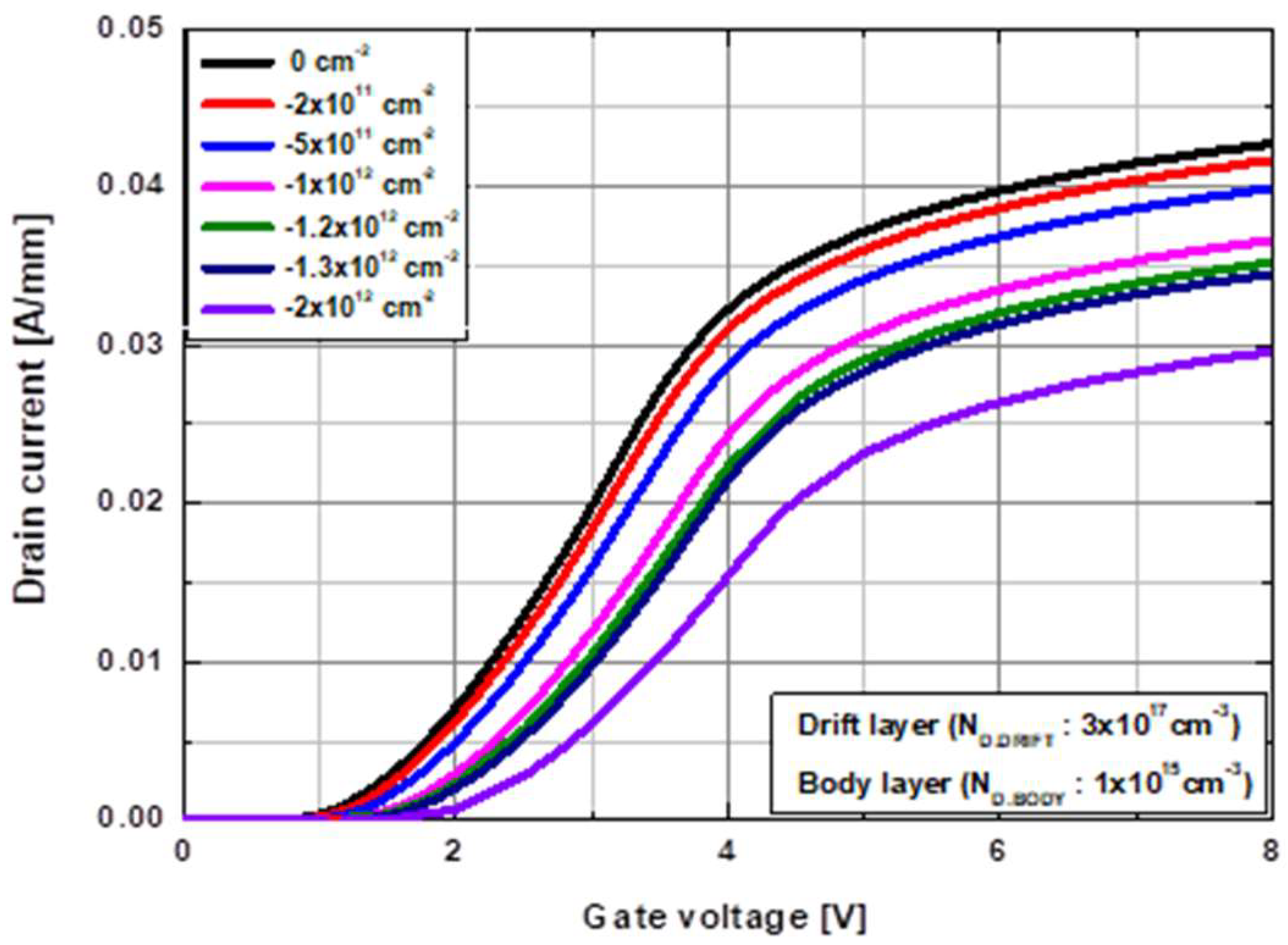
Previous studies have reported the presence of negative interface charges at the Al2O3/β-Ga2O3 interface with a density in the range of 1 × 10¹² to 4 × 1012 cm−2 [18,21,23,30,31]. In this section, the effects of charge density at the Al2O3/β-Ga2O3 interface are investigated, where the negative interface charge density varied from 0 to 2 × 1012 cm−2. The transfer characteristics simulated at a drain voltage (VDS) of 5 V as a function of the interface charge density are shown in Figure 3. A positive shift in the threshold voltage was observed with a reduction in drain current density as the negative interface charge density increased. Therefore, based on these prior experimental reports [18,20], a negative interface charge density of 1 × 1012 cm−2 was selected for the simulations.

Figure 3.
Shift in threshold voltage with different interface charge densities at the Al2O3/β-Ga2O3 interface.
3.2. Effects of Doping Concentrations in Body and Drift Layer
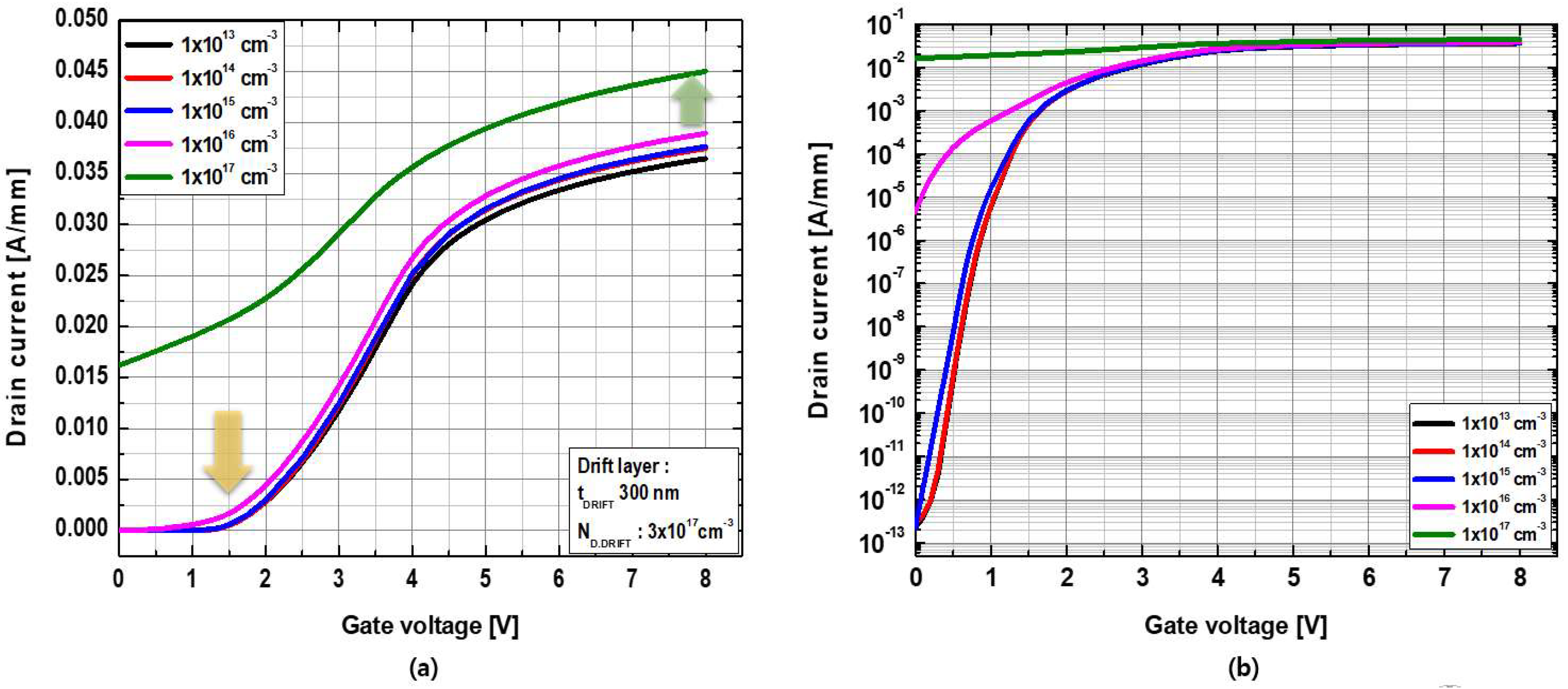
Initially, the effects of the doping concentration of the body layer (ND.BODY) on the threshold voltage were investigated. ND.BODY varied from 1 × 1013 cm−3 to 1 × 1017 cm−3, while the drift layer had a thickness of tDRIFT = 300 nm and a doping concentration of ND.DRIFT = 3 × 1017 cm−3. Figure 4a,b show the linear and logarithmic transfer characteristics at VDS = 5 V as a function of ND.BODY, respectively. A significant negative shift in the threshold voltage was observed when ND.BODY was equal to or greater than 1 × 1016 cm−3, resulting in normally-on characteristics, whereas only a negligible difference was observed when ND.BODY was equal to or less than 1 × 1015 cm−3. Therefore, to design a normally-off device, ND.BODY = 1 × 1015 cm−3 was selected for the simulations.
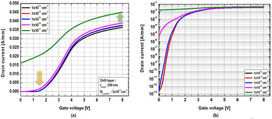
Figure 4.
(a) Linear and (b) logarithmic transfer characteristics at VDS = +5 V as a function of the doping concentration of the body layer.
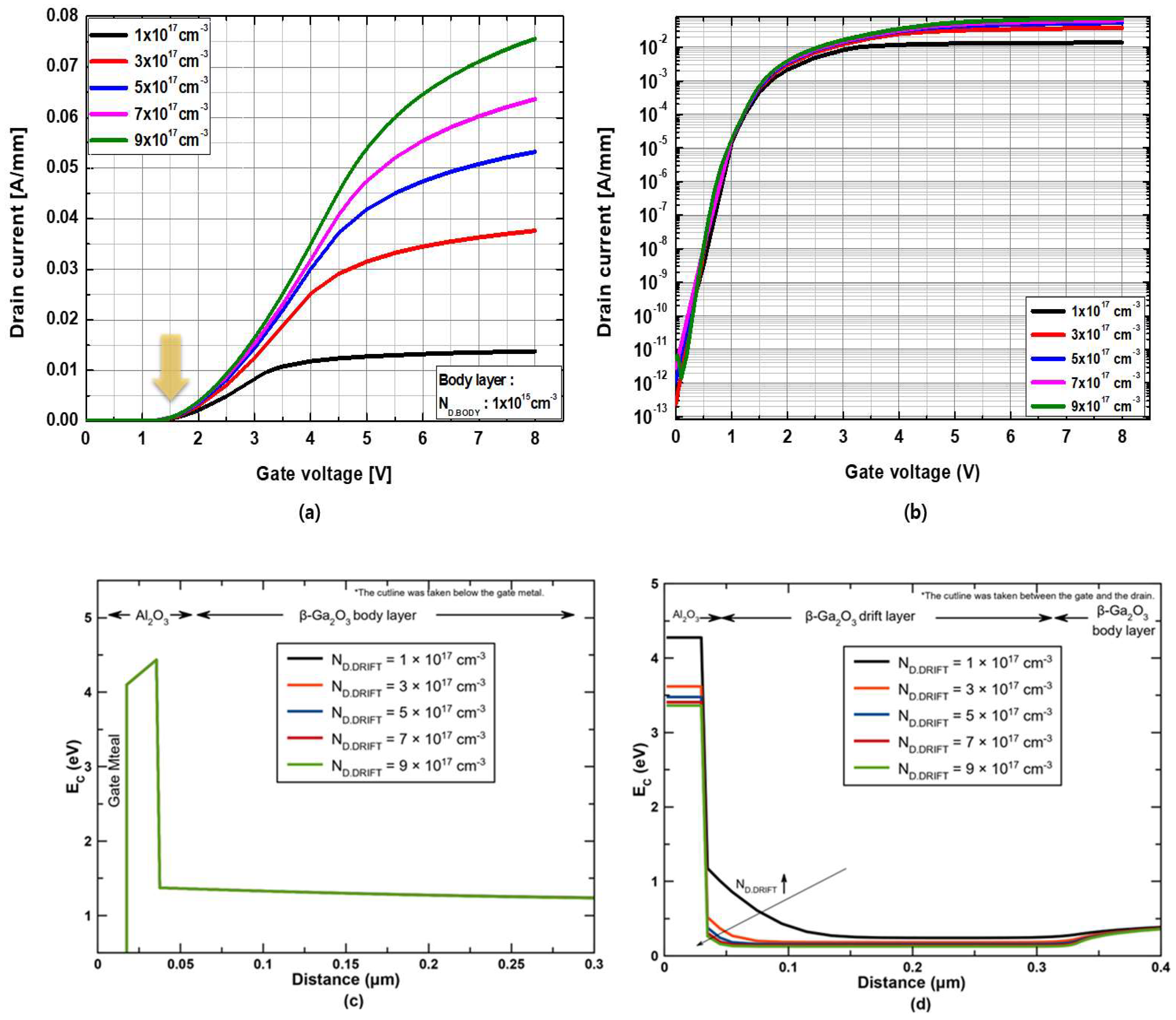
Additionally, the effects of the doping concentration of the drift layer (ND.DRIFT) on the drain current density were investigated, where ND.DRIFT varied from 1 × 1017 cm−3 to 9 × 1017 cm−3 with a fixed body doping concentration of ND.BODY = 1 × 1015 cm−3. The drift layer thickness was tDRIFT 300 nm. The transfer characteristics as a function of ND.DRIFT are shown in Figure 5a,b. It is evident that the drain current density increases with an increase in ND.DRIFT, whereas the threshold voltage remains the same because it is determined by the recessed MOS region on the body layer. The normally-off characteristics were maintained even at ND.DRIFT = 9 × 1017 cm−3. The threshold voltage was 0.8 V at 1 μA/mm and 1.5 V at 1 mA/mm. Figure 5c shows the conduction band energy diagrams as a function of ND.DRIFT along the vertical direction below the gate metal, and it is obvious that increasing ND.DRIFT does not change the conduction band energy such that the threshold voltage remains the same regardless of ND.DRIFT. On the other hand, Figure 5d shows the conduction band energy diagrams as a function of ND.DRIFT along the vertical direction in the region between the gate and drain. It can be seen that the depletion width in the β-Ga2O3 drift layer is reduced when increasing the ND.DRIFT, leading to a higher drain current.
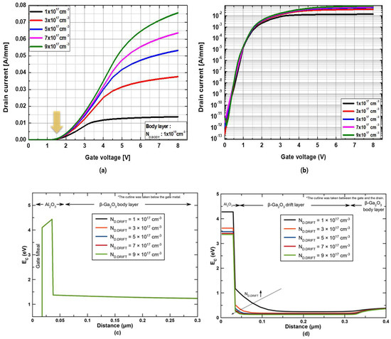
Figure 5.
(a) Linear and (b) logarithmic transfer characteristics at VDS = +5 V as a function of the doping concentration of the drift channel layer. Conduction band energy diagrams as a function of ND.DRIFT along the vertical direction (c) under the gate metal and (d) in the region between the gate and drain at zero gate bias condition.
3.3. Effects of Drift Layer Thickness
3.3.1. Transfer and Output Characteristics
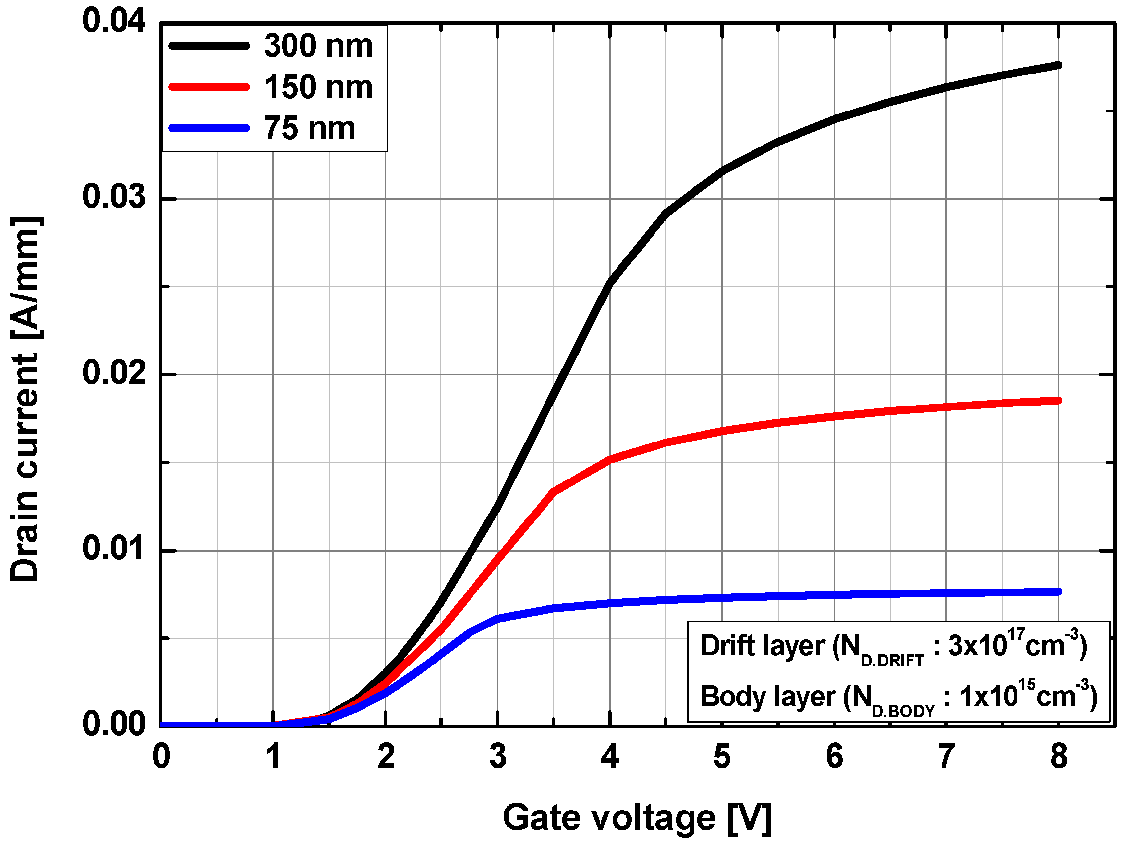
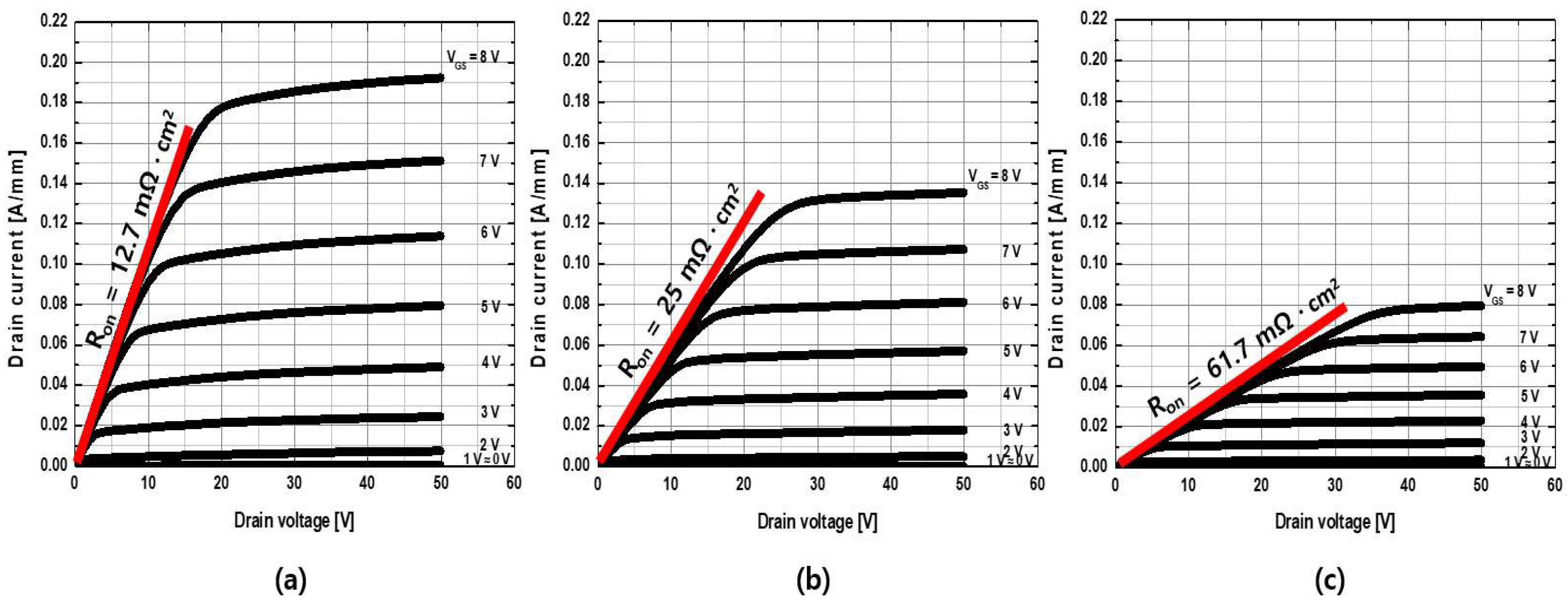
To investigate the effects of the thickness of the drift layer (tDRIFT), the doping concentrations of the body and drift channel layers were fixed as ND.BODY = 1 × 1015 cm−3 and ND.DRIFT = 3 × 1017 cm−3, respectively. The tDRIFT was varied to 75, 150, and 300 nm. As shown in Figure 6, the drain on-current density decreased with a decrease in tDRIFT, while the threshold voltage remained constant as the series resistance of the drift layer increased with a decrease in the thickness. The output current–voltage characteristics are compared in Figure 7. The maximum drain current density (ID.MAX) and on-resistance (Ron) for the thicknesses of tDRIFT = 300, 150, and 75 nm were ID.MAX = 190, 136, and 80 mA/mm, respectively, and Ron = 12.7, 25, and 61.7 mΩ cm2, respectively.

Figure 6.
Transfer characteristics at VDS = +5 V as a function of the thickness of the drift channel layer. The drift channel layer has a doping concentration of 3 × 1017 cm−3.
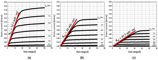
Figure 7.
Output current–voltage characteristics for a drift channel layer thickness of (a) 300 nm, (b) 150 nm, and (c) 75 nm. The drift channel layer has a doping concentration of 3 × 1017 cm−3.
3.3.2. Breakdown Characteristics
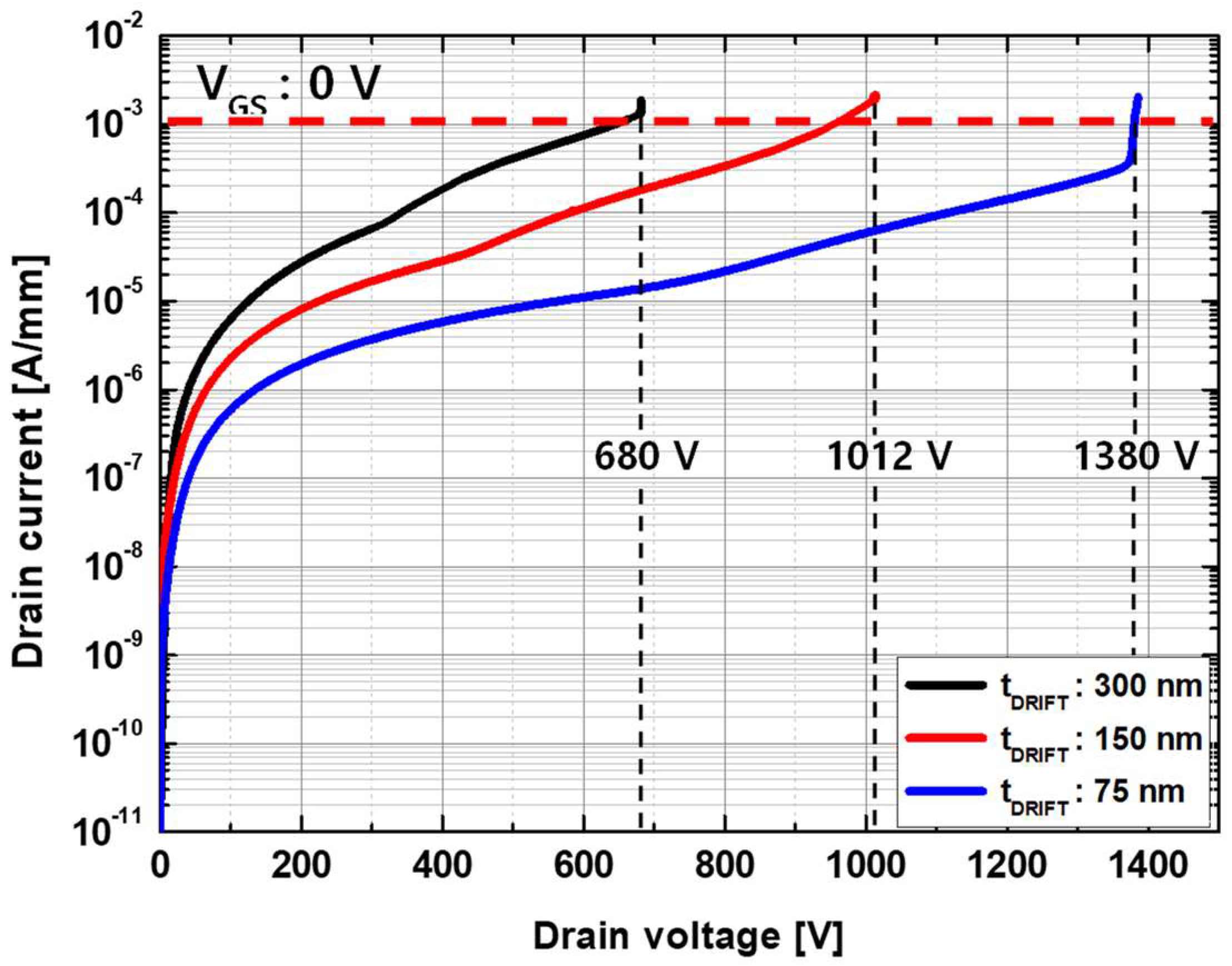
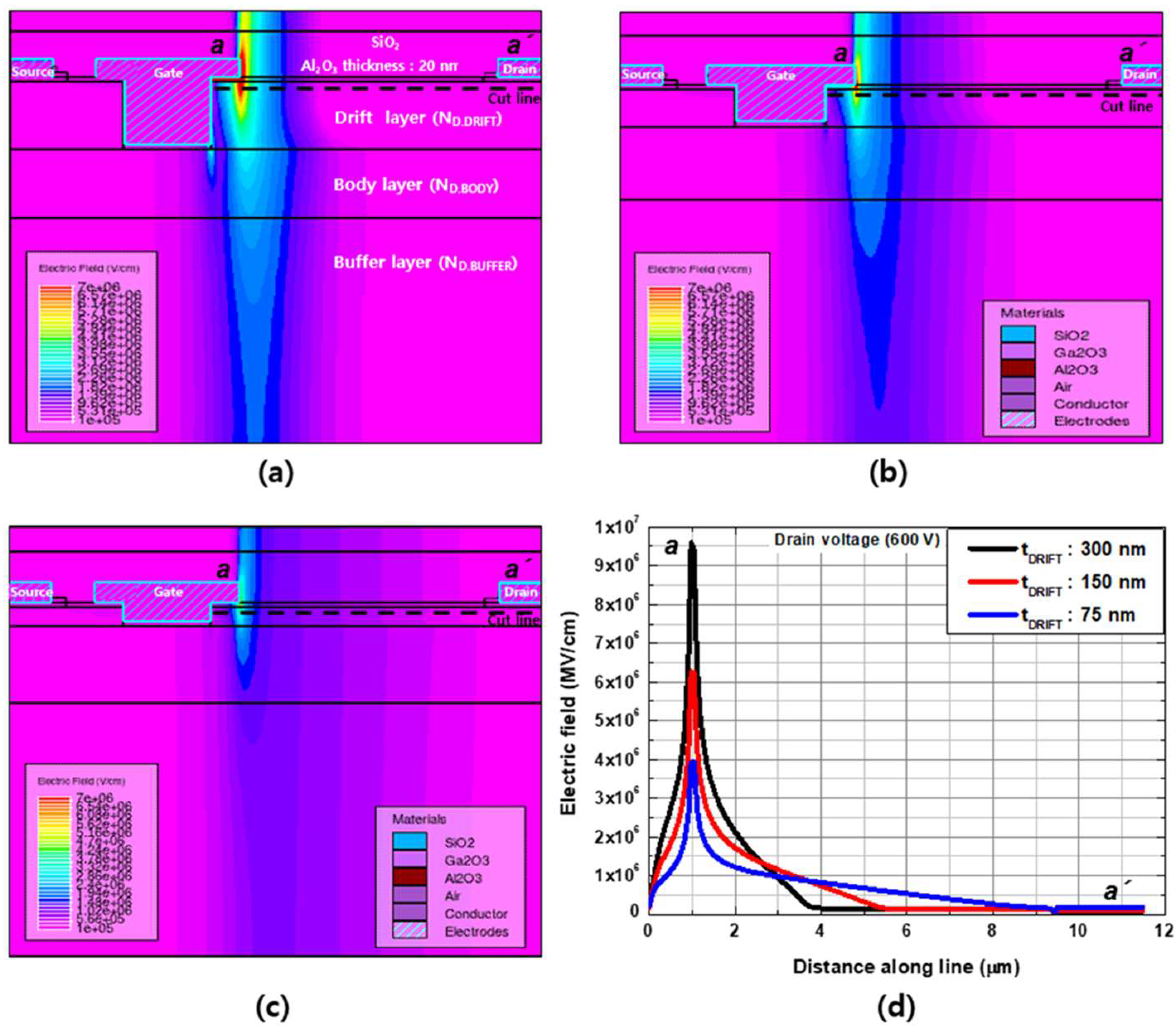
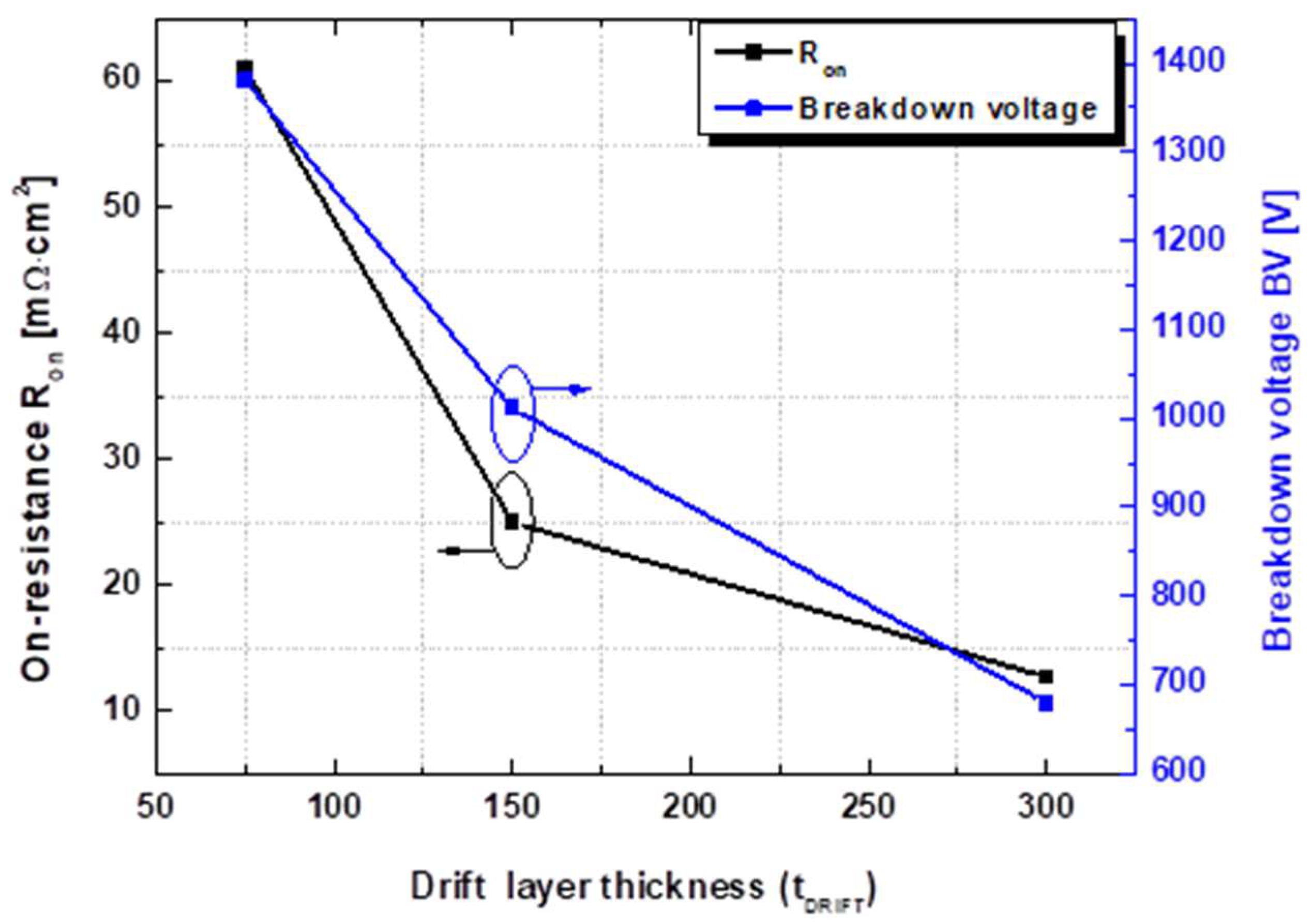
Breakdown characteristics with different drift layer thicknesses were simulated at VGS = 0 V, and the results are compared in Figure 8. The catastrophic breakdown voltages were 680, 1012, and 1380 V for the thickness values of tDRIFT = 300, 150, and 75 nm, respectively. With the same doping concentration of the drift layer, the breakdown voltage exhibited a significant dependence on tDRIFT. The electron density and electric field distributions for different tDRIFT values were examined to investigate the reasons for this. Figure 9 and Figure 10 show the electron density and electric field distributions simulated at VDS = 600 V for different tDRIFT values, and the electron concentration and electric field distributions along the cutline from a to a’ are plotted in Figure 9d and Figure 10d, respectively. As shown in Figure 9d and Figure 10d, the depletion region extended towards the drain side with decreasing thickness, resulting in a lower peak electric field near the gate. This is because the total number of electrons depleted by a given gate voltage is the same for all cases. Therefore, the thinner drift layer had a longer depletion edge. Consequently, a higher breakdown voltage can be achieved with a thinner drift layer. The tradeoff relationship between Ron and the breakdown voltage as a function of the drift layer thickness is shown in Figure 11.
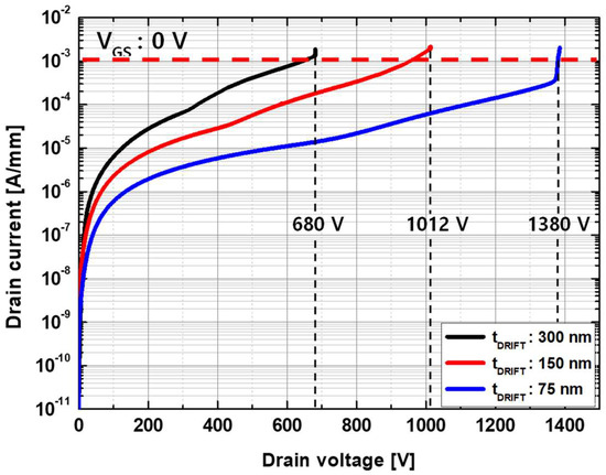
Figure 8.
Breakdown voltage characteristics simulated at VGS = 0 V as a function of the drift channel layer thickness. The drift channel layer has a doping concentration of 3 × 1017 cm−3.
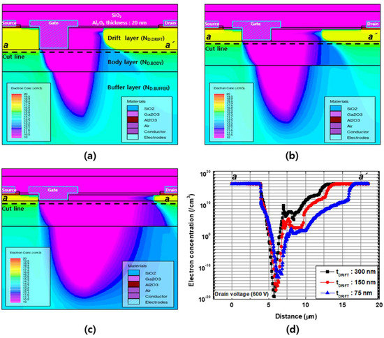
Figure 9.
Electron density distributions simulated with VGS = 0 V and VDS = + 600 V for a drift channel layer thicknesses of (a) 300 nm, (b) 150 nm, and (c) 75 nm. (d) Electron density distribution along the cutline between a and a’.
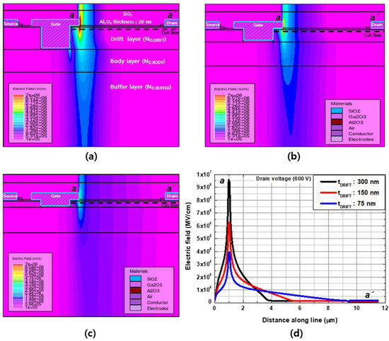
Figure 10.
Electric field distributions simulated with VGS = 0 V and VDS = +600 V for a drift channel layer thicknesses of (a) 300 nm, (b) 150 nm, and (c) 75 nm. (d) Electric field distribution along the cutline between a and a’.

Figure 11.
On-resistance and breakdown voltage characteristics as a function of drift layer thickness. The drift layer has a doping concentration of 3 × 1017 cm−3.
In summary, using a body layer with a doping concentration of 1 × 1015 cm−3 and a drift layer with a doping concentration of 3 × 1017 cm−3, a thickness of 150 nm, and a gate-to-drain distance of 9.5 μm resulted in a threshold voltage of 0.8 V at 1 μA/mm, a breakdown voltage of ~1 kV, and an on-resistance of 25 mΩ·cm2.
4. Conclusions
A normally-off β-Ga2O3 MOSFET structure was proposed, which employed an epitaxial drift layer in conjunction with a recessed MOS gate. A positive threshold voltage was achieved by employing a low-doped n-type body layer, which led to the formation of an electron-accumulation channel layer. An additional drift layer grown on top of the body layer is crucial for determining the on-resistance and breakdown voltage characteristics. The proposed dual epitaxial structure enables normally-off operation without employing an ion implantation process. Considering the difficulty of p-type ion implantation or epitaxial growth with β-Ga2O3, the proposed structure is a promising candidate for the implementation of a normally-off β-Ga2O3 FET.
Author Contributions
Investigation, C.-H.J.; methodology and software, C.-H.J. and G.A.; writing—original draft preparation, C.-H.J. and G.A.; writing—review and editing, H.-Y.C.; supervision, H.-Y.C. All authors have read and agreed to the published version of the manuscript.
Funding
This work was supported by the Technology Innovation Program (RS-2022-00154905), funded by the Ministry of Trade, Industry & Energy (MOTIE, Korea), the Basic Science Research Programs (2015R1A6A1A03031833), and Brain Pool Program through the National Research Foundation of Korea (NRF) funded by the Ministry of Science and ICT (2020H1D3A1A0410562511).
Conflicts of Interest
The authors declare no conflict of interest.
References
- Lee, I.; Kumar, A.; Zeng, K.; Singisetti, U.; Yao, X. Mixed-mode circuit simulation to characterize Ga2O3 MOSFETs in different device structures. In Proceedings of the IEEE 5th Workshop on Wide Bandgap Power Devices and Applications (WiPDA), Albuquerque, NM, USA, 30 October–1 November 2017. [Google Scholar] [CrossRef]
- Kim, K.H.; Choa, S.H. Recent overview on power semiconductor devices and package module technology. J. Microelectron. Packag. Soc. 2019, 26, 15–22. [Google Scholar] [CrossRef]
- Lv, Y.; Zhou, X.; Long, S.; Liang, S.; Song, X.; Zhou, X.; Dong, H.; Wang, Y.; Feng, Z.; Cai, S. Lateral source field-plated β-Ga2O3 MOSFET with recorded breakdown voltage of 2360 V and low specific on-resistance of 560 mΩ cm2. Semicond. Sci. Technol. 2019, 34, 11LT02. [Google Scholar] [CrossRef]
- Kim, H.S.; Mingi, J.; Cha, H.Y. Schottky barrier diode fabricated on single crystal β-Ga2O3 semiconductor. J. Inst. Electron. Inf. Eng. 2017, 54, 21–25. [Google Scholar] [CrossRef]
- Chabak, K.; Walker, D.E.; Green, A.J. Sub-Micron Gallium Oxide Radio Frequency Field-Effect Transistors. In Proceedings of the IEEE MTT-S International Microwave Workshop Series on Advanced Materials and Processes for RF and THz Applications (IMWS-AMP), Ann Arbor, MI, USA, 16–18 July 2018. [Google Scholar] [CrossRef]
- Singh, R.; Lenka, T.R.; Panda, D.K.; Velpula, R.T.; Jain, B.; Bui, H.Q.T.; Nguyen, H.P.T. The dawn of Ga2O3 HEMTs for high power electronics—A review. Mater. Sci. Semicond. Process 2020, 119, 105216. [Google Scholar] [CrossRef]
- Mun, J.K.; Cho, K.; Chang, W.; Jung, H.W.; Do, J. 2.32 kV breakdown voltage lateral β-Ga2O3 MOSFETs with source-connected field plate. ECS J. Solid State Sci. Technol. 2019, 8, Q3079. [Google Scholar] [CrossRef]
- Roberts, J.W.; Chalker, P.R.; Ding, B.; Oliver, R.A.; Gibbon, J.T.; Jones, L.A.H.; Dhanak, V.R.; Philips, L.J.; Major, J.D.; Massabuau, F.C.P. Low temperature growth and optical properties of α-Ga2O3 deposited on sapphire by plasma enhanced atomic layer deposition. J. Cryst. Growth 2019, 528, 125254. [Google Scholar] [CrossRef]
- Ren, F.; Yang, J.C.; Fares, C.; Pearton, S.J. Device processing and junction formation needs for ultra-high power Ga2O3 electronics. MRS Commun. 2019, 9, 77. [Google Scholar] [CrossRef]
- Xue, H.; He, Q.; Jian, G.; Long, S.; Pang, T.; Liu, M. An overview of the ultrawide bandgap Ga2O3 semiconductor-based schottky barrier diode for power electronics application. Nanoscale Res. Lett. 2018, 13, 290. [Google Scholar] [CrossRef]
- Ghosh, K.; Singisetti, U. Impact ionization in β-Ga2O3. J. Appl. Phys. 2018, 124, 085707. [Google Scholar] [CrossRef]
- Labed, M.; Swngouga, N.; Meftah, A.; Labed, M.; Kyoung, S.; Kim, H.; Rim, Y.S. Leakage Current Modelling and Optimization of β-Ga2O3 Schottky Barrier Diode with Ni Contact under High Reverse Voltage. ECS J. Solid State Sci. Technol. 2020, 9, 125001. [Google Scholar] [CrossRef]
- Krytsos, A.; Matsubara, M.; Bellotti, E. On the feasibility of p-type Ga2O3. Appl. Phys. Lett. 2018, 112, 032108. [Google Scholar] [CrossRef]
- Lv, Y.; Mo, J.; Song, X.; He, Z.; Wang, Y.; Tan, X.; Zhou, X.; Gu, G.; Guo, H.; Feng, Z. Influence of gate recess on the electronic characteristics of β-Ga2O3 MOSFETs. Superlattices Microstruct. 2018, 117, 132–136. [Google Scholar] [CrossRef]
- Chabak, K.D.; Moser, N.; Green, A.J.; Walker, D.E., Jr.; Tetlak, S.E.; Heller, E.; Crespo, A.; Fitch, R.; McCandless, J.P.; Leedy, K.; et al. Enhancement-mode Ga2O3 wrap-gate fin field-effect transistors on native (100) β-Ga2O3 substrate with high breakdown voltage. Appl. Phys. Lett. 2016, 109, 213501. [Google Scholar] [CrossRef]
- Chabak, K.D.; McCandless, J.P.; Moser, N.A. Recessed-gate enhancement-mode β-Ga2O3 MOSFETs. IEEE Electron Device Lett. 2018, 39, 67–70. [Google Scholar] [CrossRef]
- Singh, R.; Lenka, T.R.; Velpula, R.T.; Thang, B.H.Q.; Nguyen, H.P.T. Investigation of E-mode beta-gallium oxide MOSFET for emerging nanoelectronics. In Proceedings of the IEEE 14th Nanotechnology Materials and Devices Conference, Stockholm, Sweden, 27–30 October 2019; Volume 27–30. [Google Scholar] [CrossRef]
- Lv, Y.; Liu, H.; Zhou, X.; Wang, Y.; Song, X.; Cai, Y.; Yan, Q.; Wang, C.; Liang, S.; Zhang, J.; et al. Lateral β-Ga2O3 MOSFETs With High-Power Figure of Merit of 277 MW/cm2. IEEE Electron Device Lett. 2020, 41, 537. [Google Scholar] [CrossRef]
- Wong, M.H.; Nakata, Y.; Kuramata, A.; Yamakoshi, S.; Higashiwaki, M. Enhancement-mode Ga2O3 MOSFETs with Si-ion-implanted source and drain. Appl. Phys. Express 2017, 10, 041101. [Google Scholar] [CrossRef]
- Park, J.; Hong, S.M. Simulation study of enhancement mode multi-gate vertical gallium oxide MOSFETs. ECS J. Solid State Sci. Technol. 2019, 8, Q31116. [Google Scholar] [CrossRef]
- Huang, X.; Liao, F.; Li, L.; Liang, X.; Liu, Q.; Zhang, C.; Hu, X. 3.4 kV breakdown voltage Ga2O3 trench Schottky diode with optimized trench corner radius. ECS J. Solid State Sci. Technol. 2020, 9, 045012. [Google Scholar] [CrossRef]
- Choi, J.H.; Cho, C.-H.; Cha, H.-Y. Design consideration of high voltage Ga2O3 vertical Schottky barrier diode with field plate. Results Phys. 2018, 9, 1170. [Google Scholar] [CrossRef]
- Madadi, D.; Orouji, A.A. Investigation of Short Channel Effects in SOI MOSFET with 20 nm Channel Length by a β-Ga2O3 Layer. ECS J. Solid State Sci. Technol. 2020, 9, 045002. [Google Scholar] [CrossRef]
- Silvaco Atlas User’s Manual Device Simulation Software; SILVACO International: Santa Clara, CA, USA, 2012; 169p.
- Caughey, D.; Thomas, R. Carrier mobilities in silicon empirically related to doping and field. Proc. IEEE 1967, 55, 2192–2193. [Google Scholar] [CrossRef]
- Shockley, W.; Read, W.T. Statistics of the Recombinations of Holes and Electrons. Phys. Rev. 1952, 87, 835. [Google Scholar] [CrossRef]
- Khodadadiana, A.; Parvizia, M.; Heitzinger, C. An adaptive multilevel Monte Carlo algorithm for the stochastic drift-diffusion-Poisson system. Comput. Methods Appl. Mech. Eng. 2020, 368, 113163. [Google Scholar] [CrossRef]
- Poncé, S.; Li, W.; Reichardt, S.; Giustino, F. First-principles calculations of charge carrier mobility and conductivity in bulk semiconductors and two-dimensional materials. Rep. Prog. Phys. 2020, 83, 036501. [Google Scholar] [CrossRef] [PubMed]
- Parisini, A.; Fornari, R. Analysis of the scattering mechanisms controlling electron mobility in β-Ga2O3 crystals. Semicond. Sci. Technol. 2016, 31, 035023. [Google Scholar] [CrossRef]
- Tetzner, K.; Treidel, E.B.; Hilt, O.; Popp, A.; Anooz, S.B.; Wagner, G.; Thies, A.; Ickert, K.; Gargouri, H.; Wurfl, J. Lateral 1.8 kV β-Ga2O3 MOSFET with 155 MW/cm2 power figure of merit. IEEE Electron Device Lett. 2019, 40, 1503. [Google Scholar] [CrossRef]
- Hung, T.-H.; Sasaki, K.; Kuramata, A.; Nath, D.N.; Park, P.S.; Polchinski, C.; Rajan, S. Energy band line-up of atomic layer deposited Al2O3 on β-Ga2O3. Appl. Phys. Lett. 2014, 104, 162106. [Google Scholar] [CrossRef]

Publisher’s Note: MDPI stays neutral with regard to jurisdictional claims in published maps and institutional affiliations. |
© 2022 by the authors. Licensee MDPI, Basel, Switzerland. This article is an open access article distributed under the terms and conditions of the Creative Commons Attribution (CC BY) license (https://creativecommons.org/licenses/by/4.0/).