Abstract
The measurements of wafers’ surface profile are crucial for safeguarding the fabrication quality of integrated circuits and MEMS devices. The current techniques measure the profile mainly by moving a capacitive or optical spacing sensing probe along multiple lines, which is high-cost and inefficient. This paper presents the calculation, simulation and experiment of a method for measuring the surface profile with arrayed capacitive spacing transducers. The calculation agreed well with the simulation and experiment. Finally, the proposed method was utilized for measuring the profile of a silicon wafer. The result is consistent with that measured by a commercial instrument. As a movement system is not required, the proposed method is promising for industry applications with superior cost and efficiency to the existing technology.
1. Introduction
Silicon wafers are widely used in the fabrication process of integrated circuits (IC) and MEMS devices [1,2]. The wafer residual stress is remarkable for the following reasons: The thin pancake-like shape of the wafer, the multiple-layer structure with a different coefficient of thermal expansion (CTE), and the high-temperature fabrication process such as thermal oxidation, hard bake of photoresist, annealing and bonding process [3,4,5,6,7]. The combined effects of the induced residual stresses acting on the backside and frontside of the wafer result in wafer warpage [8]. More recently, larger silicon wafers are always preferred for reducing the cost of a single IC or MEMS device further. Moreover, ultrathin silicon die is a key enabler for high performance semiconductor devices and ultrathin packaging including three-dimensional packages. As a result, measuring the surface profile of the wafers is crucial for safeguarding the precision and reliability of the fabracated IC and MEMS devices [9,10,11,12]. In addition, the measured warpage can also be used for analyzing the residual stress, which is crucial for evaluating the creep property of the fabricated chips. In cases of serious warpage, the wafers will be discarded for saving cost and time in future processing [13].
The main technique for measuring the surface profile of wafers is moving a capacitive or optical spacing sensing probe along multiple lines on the surface of silicon wafers [14,15]; however, the system is complex, high-cost and inefficient. What is more, the complicated multi-axis motorized position system is difficult to integrate with processing equipment for in-suit measurements. Another technique is the optical plane interferometer [16,17,18]. As surface interference has no requirements for moving probes, this method is efficient. However, the measurement precision is limited by the flatness of the reference mirror, which is difficult to fabricate for the large area of the wafer.
In this work, we present a technique for measuring the surface profile of the silicon wafer with arrayed capacitive spacing transducers on a flat glass wafer. The main technology findings include: (1) Through measuring the spacing between the silicon wafer and the glass wafer on multiple grids with arrayed capacitive spacing transducers, the surface profile of the silicon wafer can be fitted without the requirement for an additional movement system. As a result, the system is efficient and easier to integrate into processing machines for in situ measurements. (2) The design of the capacitive transducer with two electrodes on the glass wafer is able to detect the spacing with no need for signal connection to the wafers to be detected, thus simplifying the measurement system. Beneficial from the above innovations, the proposed method is promising for industry applications with superior cost and efficiency to the existing technology.
2. Design
A capacitive displacement transducer is composed of two metal electrodes (E1 and E2) deposited on the glass wafer and one electrode formed by the silicon wafer to be measured (E0), as shown in Figure 1.

Figure 1.
Schematic of a capacitive spacing transducer.
Based on the planar plate capacitor model, the capacitances can be calculated by:
where ε is the dielectric constant of air, S is the area of the electrodes (E1 and E2), and d is the spacing between E1 and E0. The total capacitance of the two series connected capacitors is:
As the capacitance measurement precision (ΔC) of the LCR meter is 0.1% of the capacitance to be measured, the precision of the capacitive displacement transducer (Δd) can be evaluated by:
When parasitic capacitance (Cf) is considered, the actual measured capacitance can be expressed as:
It can be derived from Equation (4) that the spacing between the E1 and E0 is
It reveals that the spacing can be calculated via measuring the capacitances C and Cf.
In order to measuring the surface profile of the wafer, arrayed electrodes are deposited on a flat glass wafer, as shown in Figure 2. The spacing of every capacitive transducer is calculated according to Equation (5).
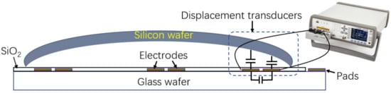
Figure 2.
Schematic of multi-grid capacitive transducers for measuring wafer surface profile.
The glass wafer was fabricated with typical micromachining processes, as shown in Figure 3. Firstly, a double-layer photoresist was patterned. Then a 40 nm Ti layer and a 200 nm Au layer were deposited with an electron beam evaporation, followed by a lift-off process for patterning the electrodes. Then, another photoresist layer was patterned, covering the pads that are used to connect the LCR meter. Afterwards, a 300 nm SiO2 layer was deposited with PECVD for electric insulation. Finally, a wet etching with organic solvent removed the photoresist and the SiO2 adhered to it.

Figure 3.
Fabrication process.
The design of the surface profile measurement system is shown in Figure 4. Capacitive transducers are deposited symmetrically on a 5-inch square glass wafer for evaluating the surface profile of 4-inch silicon wafers, as shown in Figure 4a. The capacitive transducer is composed of a circular electrode and a concentric ring with the same area of 28 mm2, as shown in Figure 4b. This design is beneficial for reducing the difference between the average distances of the two electrodes to the wafer to be detected. The large electrode size is also beneficial to reduce a fringe effect that is not considered in the model of the capacitive displacement transducer. In addition, arc-shaped marks are utilized for alignment when locating the wafers to be measured.
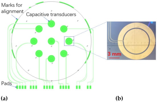
Figure 4.
Design of the surface profile measurement system. (a) The arrangement of the multi-grid capacitive transducers on a 5-inchsquare glass wafer; (b) the microscope image of a single capacitive transducer.
3. Results
3.1. Calculation, Simulation and Calibration
The relationship between the measured capacitance and the spacing is calculated according to Equation (2). A finite element analysis (FEA) simulation by Ansoft Maxwell, Ansoft Corporation, Pittsburgh, USA, is used as a reference, as shown in Figure 5. The stray capacitance was simulated in the situation that no wafer is above the electrodes. The results reveal that when correcting the stray capacitance, the simulation results agree well with that of the calculation. It could also be concluded from the results that the capacitive displacement transducer is more sensitive for measuring a smaller spacing. Considering the precision of the LCR meter for measuring capacitances is 0.1%, the precision for measuring the spacing can be calculated based on Equation (3), as shown in Figure 6.

Figure 5.
The calculation and simulation of the relationship between the measured capacitance and the spacing.

Figure 6.
Calculation of the spacing measurement precision.
When measuring the surface profile of the wafer, the electrodes are electrically connected to the LCR meter via probes, as shown in Figure 7a. In order to calibrate the capacitive displacement transducer experimentally, a flat silicon chip, whose area is slightly larger than one transducer, was installed on a high-precision displacement table. Firstly, the silicon chip was moved right above the electrodes. Then, it was moved down until contacting the surface of the electrodes. Afterwards, the silicon chip was moved upward by a step of 5 µm, 5 µm, 30 µm, 30 µm, 30 µm, 70 µm, successively. The results are shown in Figure 8 with theoretical value calculated using Equation (4) for reference. The coinciding of the experiment and calculation verified the feasibility of the capacitive spacing transducer. The calibration results were also used to calculate the spacing on every grid when measuring the surface profile of wafers.

Figure 7.
Experimental sets, (a) the experimental sets for measuring the surface profile of wafers; (b) the experimental sets for calibrating the capacitive spacing transducer.

Figure 8.
Calibration results of the capacitive spacing transducer.
3.2. Surface Profile Measurements
The warpage of the glass substrate was measured to be less than 0.5 µm by a commercial film-stress interferometer (FLX-2320-S, Toho Technology Corporation, Inazawa, Aichi, Japan), as shown in Figure 9. A 4-inch double-polished silicon wafer with a resistivity of 0.001–0.01 Ω cm was located on the surface profile measurement system, as shown in Figure 8. The capacitance of every spacing transducer was measured by moving the probe to contact the related pads. The measured capacitances were used to calculate the spacing. As a reference, the profile of the wafer was also measured by scanning along four lines on the wafer with a commercial film-stress interferometer. The results are shown in Figure 10. The tendency of the results by the proposed surface profile measurement system agrees well with that by the interferometer. Nevertheless, the errors between them can be several micrometers. The reasons could be: (1) The large area of the electrodes that influences the spatial resolution of every measurement node as the measured spacing is the average spacing of the capacitor. (2) The data of the interferometer were leveled for removing the tilting of the scanned profile, while the data by the proposed capacitive method were not able to be leveled by the same process for different spatial resolution. (3) An error induced by the resolution of the LCR meter, which was less than 0.2 µm theoretically. (4) An error induced by the warpage of the glass substrate, which was less than 0.5 µm.

Figure 9.
The surface profile of the glass substrate for the capacitive transducers array along orthorhombic directions.
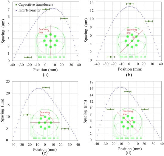
Figure 10.
Measured wafer surface profile by the proposed capacitive transducers. The measurement results by a commercial film-stress interferometer are shown as a reference. (a) The scanning line is parallel to the reference line; (b) The angle between the scanning line and the reference line is 45 degrees; (c) The angle between the scanning line and the reference line is 90 degrees; (d) The angle between the scanning line and the reference line is 135 degrees.
4. Discussion
This paper proposed a surface profile measurement system without the requirement on movement systems, and the proposed method is inexpensive and convenient compared with current techniques. Moreover, the system is easy to be packaged into processing equipment, which is promising to in situ measurements for industry applications.
The proposed surface profile measurement system is only a demo for verifying the feasibility of the design. The errors can be several micrometers, which are not suitable for high-precision applications. In terms of measuring precision, the system can be further improved via the following means: (1) Improving the spatial resolution of the capacitive spacing transducers. For reducing the fringe effect, the dimension of the electrode should be at least three times larger than the spacing [19]. As a result, for measuring a warpage of less than 200 μm, the diameter of the electrode could be designed to be 600 μm, which is 10 times less than the present design. (2) As the dimension of the electrode is reduced, the density of the arrayed capacitive transducers can be increased, which is also beneficial for improving the spatial resolution. (3) Utilizing multichannel capacitance measuring circuits to measure the capacitance of all the capacitive transducers at the same time with higher precision and efficiency. (4) Choosing glass wafer with less original warpage.
Author Contributions
Methodology, P.Z.; software, B.C.; validation, T.Z.; formal analysis, L.Y.; writing—original draft preparation, P.Z. and T.Z.; writing—review and editing, W.W. and L.T.; supervision, L.T.; project administration, W.W.; funding acquisition, W.W. All authors have read and agreed to the published version of the manuscript.
Funding
This research was funded in part by the National Key Research and Development Program of China under Grant 2021YFB3201601, and in part by the National Natural Science Foundation of China under Grant 42274230.
Data Availability Statement
Not applicable.
Acknowledgments
We thank the Center of Micro-Fabrication and Characterization (CMFC) of Wuhan National Laboratory for Optoelectronics (WNLO) at Huazhong University of Science and Technology (HUST) for the device fabrication support.
Conflicts of Interest
The authors declare no conflict of interest.
References
- Petersen, K.E. Silicon as a Mechanical Material. Proc. IEEE 1982, 70, 420–457. [Google Scholar] [CrossRef]
- Yeap, K.H.; Nisar, H.; Dakulagi, V. Warpage Reduction for Power Mosfet Wafers. Electrica 2021, 21, 173–179. [Google Scholar] [CrossRef]
- Chu, W.; Rashidi, S.E.E.; Zhang, Y.; Alsmeier, J.; Sega, T. An Analytical Model for Thin Film Pattern-Dependent Asymmetric Wafer Warpage Prediction. In Proceedings of the 2022 IEEE International Memory Workshop, Dresden, Germany, 15–18 May 2022; pp. 2–5. [Google Scholar]
- Cheng, G.; Xu, G.; Gai, W.; Luo, L. Reduce the Wafer Warpage Introduced by Cu in RDL Through Adjusting the Cooling Temperatures. In IEEE 68th Electronic Components and Technology Conference, San Diego, CA, USA, 29 May 2018; pp. 669–674. [Google Scholar] [CrossRef]
- Li, H.; Zhu, C.; Xu, G.; Luo, L. Experimental Identification of Thermal Induced Warpage in Polymer-Metal Composite Films. Microelectron. Reliab. 2016, 62, 141–147. [Google Scholar] [CrossRef]
- Yeon, S.; Park, J.; Lee, H.J. Compensation Method for Die Shift Caused by Flow Drag Force in Wafer-Level Molding Process. Micromachines 2016, 7, 95. [Google Scholar] [CrossRef] [PubMed]
- Yazdi, S.A.F.F.; Garavaglia, M.; Ghisi, A.; Corigliano, A. A New Approach for the Control and Reduction of Warpage and Residual Stresses in Bonded Wafer. Micromachines 2021, 12, 361. [Google Scholar] [CrossRef] [PubMed]
- Marks, M.R.; Hassan, Z.; Cheong, K.Y. Characterization Methods for Ultrathin Wafer and Die Quality: A Review. IEEE Trans. Compon. Packaging Manuf. Technol. 2014, 4, 2042–2057. [Google Scholar] [CrossRef]
- Wu, X.; Tay, A. Influence of Wafer Warpage on Photoresist Film Thickness and Extinction Coefficient Measurements. Metrol. Insp. Process Control. Microlithogr. XXI 2007, 6518, 1446–1453. [Google Scholar] [CrossRef]
- Zhu, C.; Lee, H.; Ye, J.; Xu, G.; Luo, L. A New Designed Trench Structure to Reduce the Wafer Warpage in Wafer Level Packaging Process. In Proceedings of the Electronic Packaging Technology Conference, Chengdu, China, 12–15 August 2014; pp. 606–609. [Google Scholar] [CrossRef]
- Zhu, C.; Ning, W.; Xu, G.; Luo, L. Stress Evolution during Thermal Cycling of Copper/Polyimide Layered Structures. Mater. Sci. Semicond Process. 2014, 27, 819–826. [Google Scholar] [CrossRef]
- Zhu, C.; Ning, W.; Lee, H.; Ye, J.; Xu, G.; Luo, L. Experimental Identification of Warpage Origination during the Wafer Level Packaging Process. In Proceedings-Electronic Components and Technology Conference, Orlando, FL, USA, 27–30 May 2014; pp. 815–820. [Google Scholar] [CrossRef]
- Tay, A.; Ho, W.K.; Hu, N.; Chen, X. Estimation of Wafer Warpage Profile during Thermal Processing in Microlithography. Rev. Sci. Instrum. 2005, 76, 1–8. [Google Scholar] [CrossRef]
- Ku, Y.S.; Shyu, D.M.; Chang, P.Y.; Hsu, W.T. In-Line Metrology of 3D Interconnect Processes. Metrol. Insp. Process. Control. Microlithogr. XXVI 2012, 8324, 1–8. [Google Scholar] [CrossRef]
- Tahara, K.; Matsuoka, H.; Morioka, N.; Kannaka, M. Site Flatness Measurement System with Accuracy of Sub-Nanometer Order for Silicon Wafer. Kobelco Technol. Rev. 2016, 34, 59–64. [Google Scholar]
- Riedel, F.; Gerber, H.A.; Wagner, P. Impact of Filtering on Nanotopography Measurement of 300 Mm Silicon Wafers. Mater. Sci. Semicond. Process. 2002, 5, 465–472. [Google Scholar] [CrossRef]
- Galas, J.; Litwin, D.; Sitarek, S.; Surma, B.; Piatkowski, B.; Miros, A. Interferometric and Confocal Techniques for Testing of Silicon Wafers. In Proceedings of the Optical Micro- and Nanometrology in Microsystems Technology; SPIE, Strasbourg, France, 21 April 2006; pp. 1–8. [Google Scholar]
- Yang, K.H. Optical Imaging Method for Wafer Warpage Measurements. Electrochem. Soc. Ext. Abstr. 1985, 132, 1214. [Google Scholar] [CrossRef]
- Wu, W.; Zheng, P.; Liu, J.; Li, Z.; Fan, J.; Liu, H.; Tu, L. High-Sensitivity Encoder-like Micro Area-Changed Capacitive Transducer for a Nano-g Micro Accelerometer. Sensors 2017, 17, 1–17. [Google Scholar] [CrossRef] [PubMed]


Disclaimer/Publisher’s Note: The statements, opinions and data contained in all publications are solely those of the individual author(s) and contributor(s) and not of MDPI and/or the editor(s). MDPI and/or the editor(s) disclaim responsibility for any injury to people or property resulting from any ideas, methods, instructions or products referred to in the content. |
© 2022 by the authors. Licensee MDPI, Basel, Switzerland. This article is an open access article distributed under the terms and conditions of the Creative Commons Attribution (CC BY) license (https://creativecommons.org/licenses/by/4.0/).