Article

High Oxygen Sensitivity of TiO2 Thin Films Deposited by ALD

by
Aleksei V. Almaev
1,2,*,
Nikita N. Yakovlev
1,
Dmitry A. Almaev
1,
Maksim G. Verkholetov
1,3,
Grigory A. Rudakov
3 and
Kristina I. Litvinova
3
1
Research and Development Center for Advanced Technologies in Microelectronics, National Research Tomsk State University, 634050 Tomsk, Russia
2
Fokon LLC, 248035 Kaluga, Russia
3
Institute of Nanotechnology of Microelectronics of the Russian Academy of Sciences, 119991 Moscow, Russia
*
Author to whom correspondence should be addressed.
Micromachines 2023, 14(10), 1875; https://doi.org/10.3390/mi14101875
Submission received: 12 September 2023 / Revised: 27 September 2023 / Accepted: 28 September 2023 / Published: 29 September 2023
(This article belongs to the Special Issue Advanced Thin-Films: Design, Fabrication and Applications)

Abstract

:
The gas sensitivity and structural properties of TiO2 thin films deposited by plasma-enhanced atomic layer deposition (ALD) were examined in detail. The TiO2 thin films are deposited using Tetrakis(dimethylamido)titanium(IV) and oxygen plasma at 300 °C on SiO2 substrates followed by annealing at temperatures of 800 °C. Gas sensitivity under exposure to O2 within the temperature range from 30 °C to 700 °C was studied. The ALD-deposited TiO2 thin films demonstrated high responses to O2 in the dynamic range from 0.1 to 100 vol. % and low concentrations of H2, NO2. The ALD deposition allowed the enhancement of sensitivity of TiO2 thin films to gases. The greatest response of TiO2 thin films to O2 was observed at a temperature of 500 °C and was 41.5 arb. un. under exposure to 10 vol. % of O2. The responses of TiO2 thin films to 0.1 vol. % of H2 and 7 × 10⁻⁴ vol. % of NO2 at a temperature of 500 °C were 10.49 arb. un. and 10.79 arb. un., correspondingly. The resistance of the films increased due to the chemisorption of oxygen molecules on their surface that decreased the thickness of the conduction channel between the metal contacts. It was suggested that there are two types of adsorption centers on the TiO2 thin films surface: oxygen is chemisorbed in the form of O2– on the first one and O on the second one.

1. Introduction

Oxygen is the most important gas for human life, and there is a widespread demand for O2 sensors and for measuring the O2 concentration in ambient environment. Oxygen detection at an over 1 vol. % level with a high accuracy is essential to control the reactive chemical concentration in the chemical industry and metallurgy [1] and to analyze exhaust gas composition of automobile engines [2,3].
TiO2 belongs to the large material class of metal oxide semiconductors [4,5,6,7,8,9,10]. It is attractive for developing O2 sensors due to its low cost and high chemical and thermal stability [11,12,13,14,15,16,17,18,19,20,21]. Now, commercial O2 sensors are based on bulk and thick-film TiO2 structures [6]. Such structures are not highly sensitive to O2. A well-known method for optimizing gas-sensitive properties of materials is the use of thin film structures [16]. Film thickness d plays a key role in the gas sensitivity of thin film structures. It has been shown that the optimal thickness of TiO2 films providing a high gas sensitivity should be comparable to the Debye length LD. The LD = 10–50 nm for TiO2 at an electron concentration of n = 1016–1018 cm−3 and a permittivity of ε0 = 18.9. Atomic layer deposition (ALD) is a highly promising method for growing very thin TiO2 films (d = 10–50 nm) with large homogeneity and reproducibility of structural and electrical properties. The ALD allows deposition of continuous films with high precision control over thickness and impurities levels [21,22].
Previously, the ALD method was used to produce thin films structures of various metal oxide semiconductors, mainly based on SnO2 (see Table 1). At the same time, the gas-sensitive properties of such structures were studied under the exposure to low concentrations of toxic gases and H2. Detailed studies on the O2 sensitivity of ALD-deposited metal oxide films have not been practically carried out. Therefore, the purpose of this work is to gain a deep insight into the gas-sensitive properties of the ALD-TiO2 thin films under O2 exposure and to explain them by proposing a theoretical model.
In Table 1, cg is the gas concentration; T is the operating temperature; S is the response; CNT is the carbon nanotubes; QDs is the quantum dots; IGZO is the indium gallium zinc oxide; NSs is the nanospheres; NShs is the nanosheets; P3HT is the poly(3-hexylthiophene); NWs is the nanowires; and RT is the room temperature.

2. Materials and Methods

TiO2 thin films were fabricated by the plasma-enhanced ALD technique using FlexAL ALD equipment (Oxford Instruments, Abingdon, UK). Thermally oxidized silicon plates (SiO2/Si) were used as substrates. Tetrakis(dimethylamido)titanium(IV) (TDMAT) [(CH3)2N]4Ti (99.999%) (Sigma-Aldrich, St. Louis, MO, USA) was used as the metal precursor with carrier gas of Ar (99.999%) at a flow rate of 200 cm3/min. Oxygen inductively coupled plasma (ICP) was used as an oxidizer. The discharge was excited in an oxygen atmosphere (99.999%) by a generator with a frequency of 13.56 MHz and a power of up to 300 W. The PEALD pulse durations were set at 0.8 s for TDMAT injection, 3 s for Ar purge, 3 s for exposure to plasma discharge, and 2 s for Ar purge. The growth rate at a temperature of 300 °C was 0.09 nm/cycle. The thickness of the deposited TiO2 films was 30 nm. A SENTECH Senduro spectral ellipsometer was used to estimate the thickness and the growth rate of TiO2 films at measurements in the wavelength range of 320–1800 nm.
The as-deposited TiO2 thin films were annealed at a temperature of 800 °C in an Ar atmosphere at a pressure of 2 kPa for 30 min. The rates of heating from RT to 800 °C and cooling from 800 °C to RT were 4 °C/min. The heating and cooling of samples were in an Ar atmosphere at a pressure of 2 kPa.
X-ray diffraction (XRD) was performed to determine the phase composition of the thin films and the crystal lattice parameters. XRD spectra of films were measured in a 2θ scanning mode employing a CuKa radiation operated at 45 kV and 40 mA. The X-ray source wavelength was 1.5406 Å. The microrelief of the film surface was studied by a Bruker Dimension Icon atomic force microscope (AFM). Cross-sectional images of the annealed samples were examined by a Jeol JEM 2100 PLUS transmission electron microscope (TEM) at an accelerating voltage of 200 kV in a bright field (BF) mode. The elemental composition of the films was determined by the BF-TEM mode by means of a JEOL EX-24261M1G5T energy dispersive X-ray spectroscopy (EDX) analyzer at a beam current of 1 nA.
To investigate the gas-sensitive properties, Pt contacts were deposited on the TiO2 film surface by means of vacuum deposition through a shadow mask. The plate with the film and contacts was divided into separate samples. The prepared samples were planar metal–semiconductor–metal (MSM) structures on SiO2/Si substrates (Figure 1). The interelectrode distance was kept at 1 mm. The thickness of the Pt contacts was about 330 nm.
The current–voltage (I–V) characteristics and time dependences of the sample’s resistance under the exposure to various gases were measured by means of a Keithley 2636A source meter and a sealed chamber with a Nextron MPS-CHH micro-probe station. A ceramic-type heater, installed in the sealed chamber, was used to heat the samples from RT to 700 °C with a temperature accuracy control of ±0.1 °C. The measurements were carried out under dark conditions and in a flow of dry N2, or in a gas mixture of dry N2 + dry O2. The flow rate of gas mixtures through the measurement chamber was maintained at 500 cm3/min. A pure dry air or a gas mixture of pure dry air + target gas was pumped through the chamber to examine the selectivity of the samples studied. H2, CO, CO2, NO2, NO and CH4 were selected as target gases. The source of pure dry air was a special generator. The concentration of the target gas in the mixture was controlled by a gas mixture generator with a Bronkhorst gas mass flow controller. The relative error of the gas flow rate did not exceed 1.5%. The voltage U applied to the samples during the measurements of time dependences of the resistance was kept at 3 V.

3. Results and Discussion

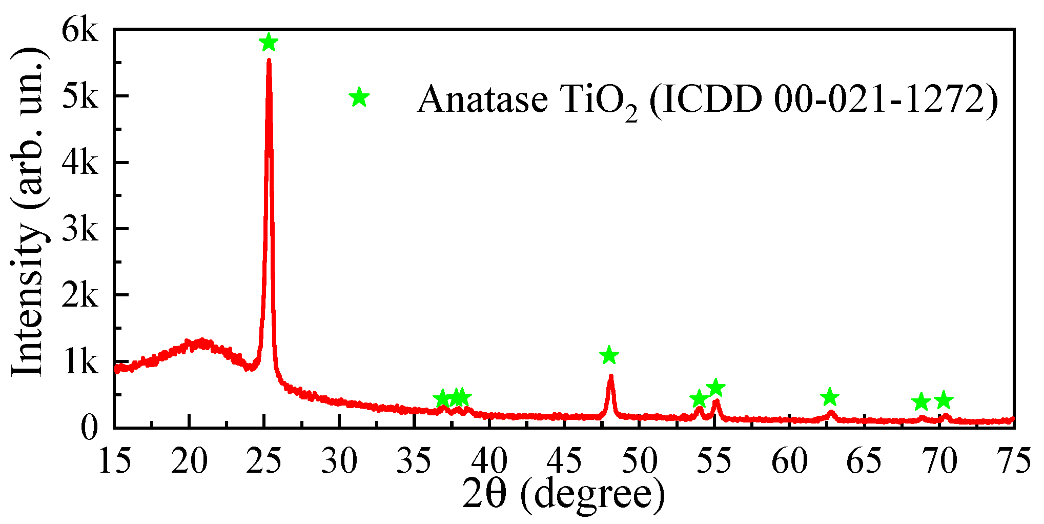
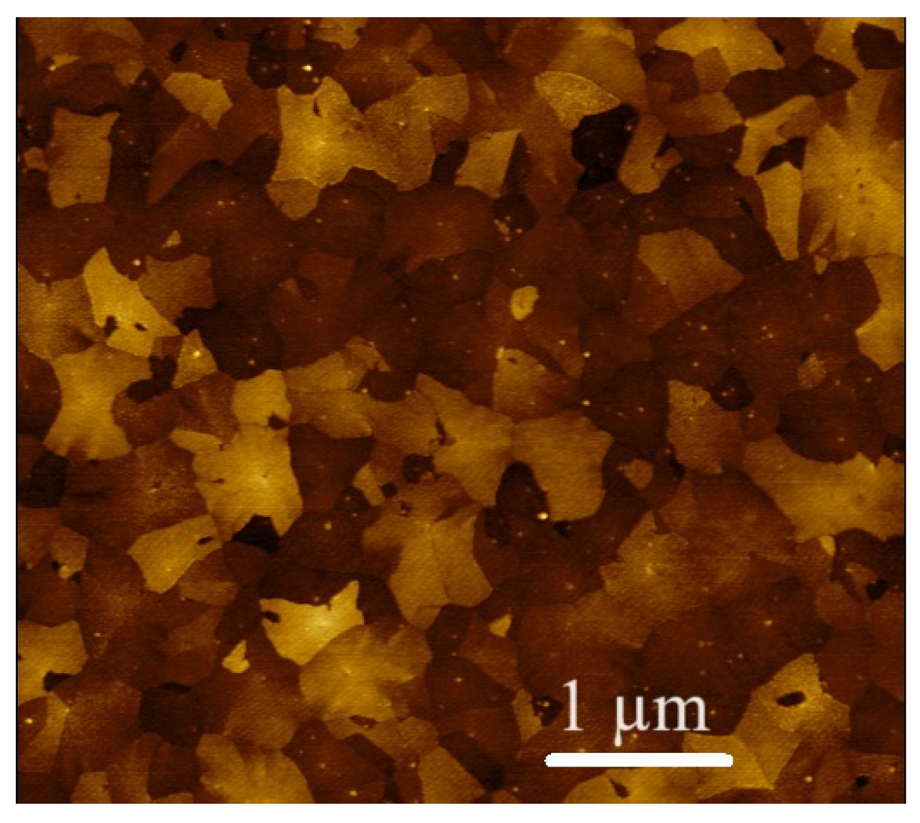
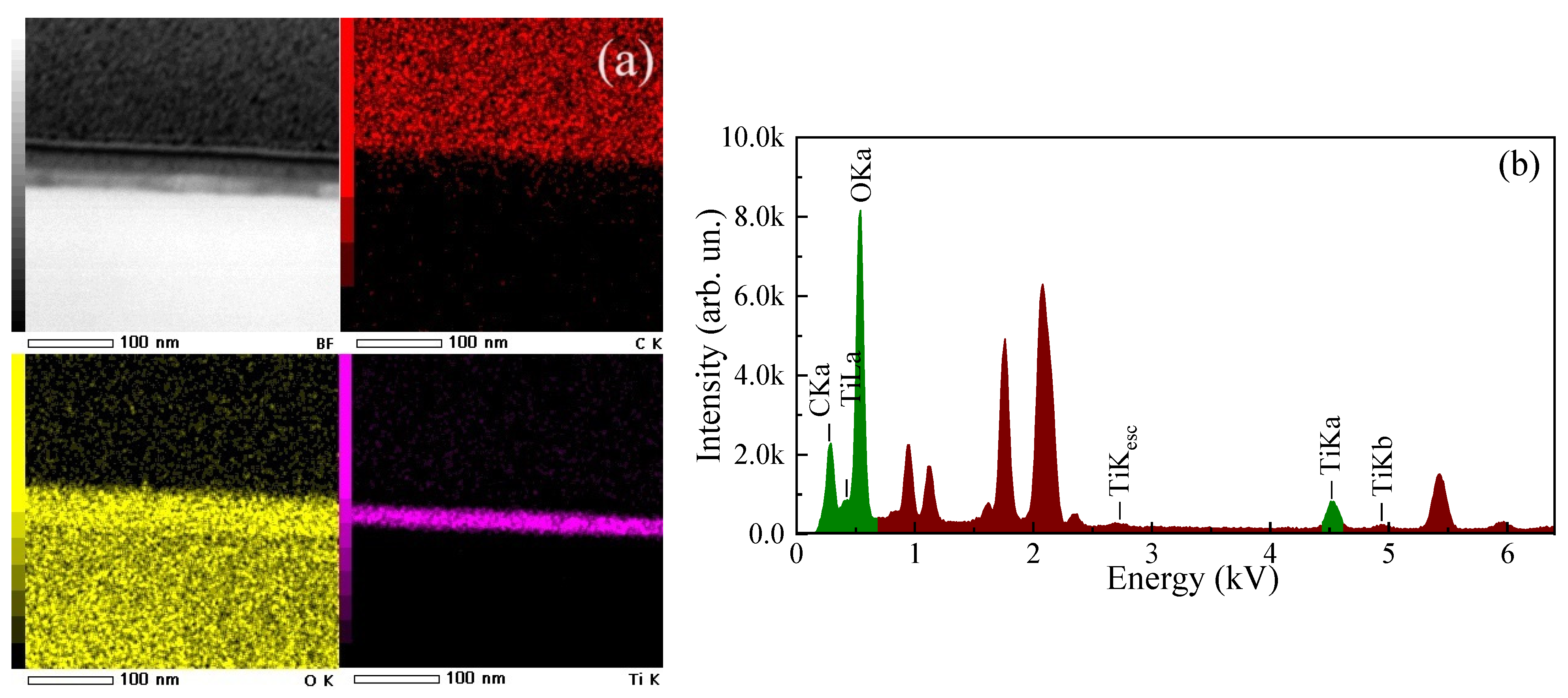
3.1. Structural Properties of the ALD-Deposited TiO2 Thin Films

Figure 2 illustrates a typical XRD spectrum of the annealed ALD-TiO2 thin film. Several peaks appear at 2θ = 25.3°, 36.9°, 37.8°, 38.2°, 48.0°, 54.0°, 55.1°, 62.7°, 68.8° and 70.3°. These peaks are associated with (101), (103), (004), (112), (200), (105), (211), (204), (116) and (220) Bragg reflections of the tetragonal anatase TiO2 phase (ICDD 00-021-1272), respectively. These results confirm the polycrystalline nature of the material grown. The wide amorphous halo at 2θ ≈ 22° is due to the SiO2 layer. The parameters of the tetragonal crystalline lattice of the film are determined as a = 3.78 Å and c = 9.50 Å.
Figure 3 depicts typical annealed ALD-TiO2 film surface morphology images taken by AFM. The surface roughness parameters of the TiO2 thin films are Ra = 1.329 nm, Rq = 1.605 nm and Rz = 12.67 nm, where Ra is the arithmetic mean of the absolute values of the deviations of the film surface profile; Rq is the mean square value of the deviations of the film surface profile and Rz is the arithmetic mean of the greatest height of the profile of the film surface. Rq is lower than the value reported in ref. [21] devoted to ALD-deposited TiO2 thin films. The relatively high surface roughness should lead to an increase in the surface-to-volume ratio and the surface density of adsorption centers for gas molecules, and, as a result of this, to an increase in responses to gases [35].
Figure 4 illustrates a BF-TEM cross-sectional image of annealed ALD-TiO2 thin film on a substrate in the high-resolution mode. The interplane distance D corresponding to the (101) reflection of the anatase TiO2 phase is 0.353 nm, determined by fast Fourier transformation (FFT). The D values for the same plane determined by FFT and by analysis of the XRD pattern (0.352 nm) are the same. TiO2 thin films have a nanocrystalline structure with amorphous inclusions according to the TEM study.
The contents of Ti and O elements in the films are measured to be ~27 at. % and ~73 at. % (Figure 5a,b), respectively. The increased O content in the films may be associated with features of the ALD process. There is also a peak corresponding to C in the EDX spectrum caused by the technological operations before the measurements of the spectrum.

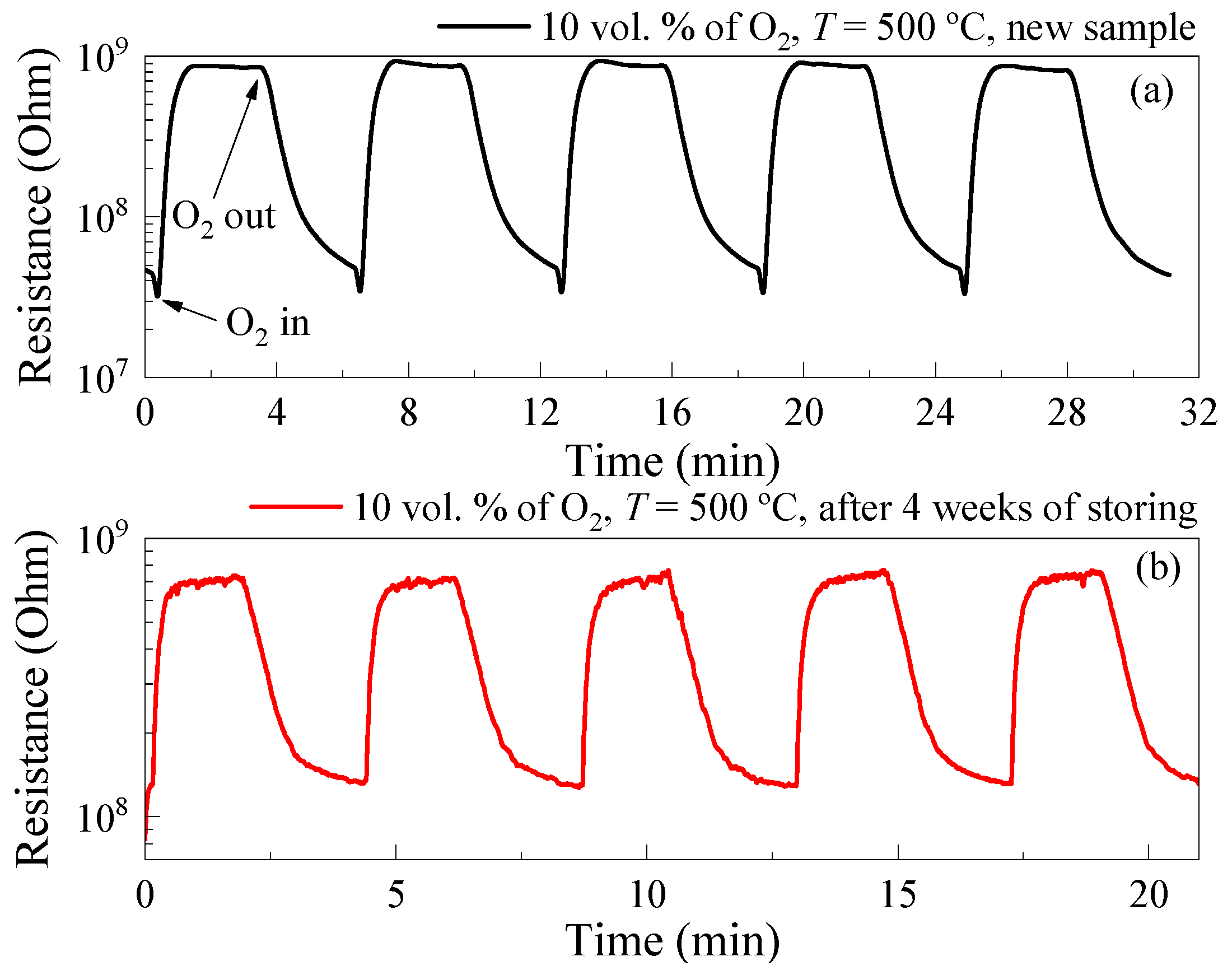
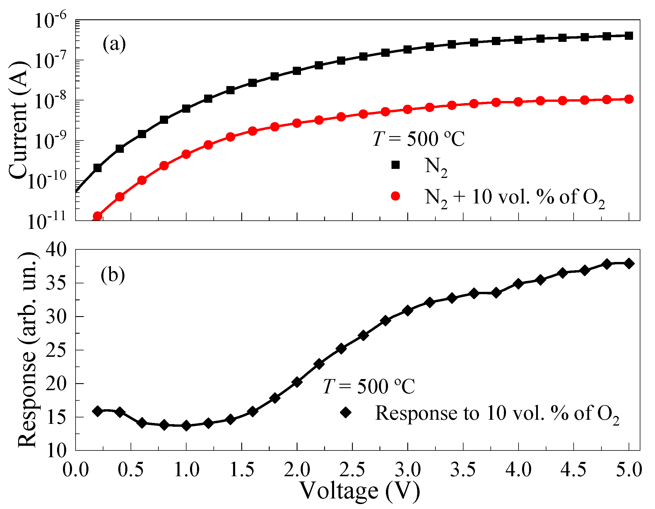
3.2. Gas-Sensetive Properties of the ALD-Deposited TiO2 Thin Films

At the next stage, the gas-sensitive properties of the ALD synthesized TiO2 thin films were investigated in detail. The exposure to O2 led to a reversible increase in the resistance of TiO2 thin films. The following ratio was chosen as the response Sox of samples to O2:
Sox = Rox/RN,
where Rox is the resistance of TiO2 thin film in a gas mixture of dry N2 + dry O2; RN is the resistance of TiO2 thin film in dry N2 atmosphere. The temperature dependencies of the responses under the exposure to 10 vol. % and 40 vol. % of O2 (Figure 6a) had a maximum at T = 500 °C.
The samples practically did not react when exposed to O2 and had a high resistance, making it impossible to reliably register the response to gases at T < 450 °C. The presence of a maximum on the temperature dependence of the response is due to the influence of temperature on the processes of dissociation, adsorption/desorption of O2 molecules, and is specific to metal oxide semiconductors [36,37]. The response tres and recovery trec times were determined upon exposure to 10 vol. % of O2 according to the method described in ref. [38] to estimate the operation speed of the films studied. The obtained values of tres and trec can only be used to compare the operation speed of sensors under similar experimental conditions. We note that the tres and trec decrease exponentially with the increase in T (see Figure 6b). It is also worth noting that tres and trec were practically the same at T = 450–700 °C. The tres and trec did not exceed 30 s in the range of T = 600–700 °C. The tres and trec were 51.5 s and 52.9 s, respectively, at temperature of the maximum response to O2.
Rox and RN decreased by 4% and 36%, correspondingly, during a cyclic exposure to 10 vol. % of O2 (five cycles) (illustrated in Figure 7a); as a result, Sox increased by 50%. On the other hand, the response of the films to O2 decreased by 6–7 times during storing in a sealed box at RT after the experiments at high T (Figure 7b) mainly due to a significant increase in RN. The healing of oxygen vacancies in TiO2 may be the reason for the increase in RN at high T and exposure to high O2 concentrations [39]. This process is inertial and, consequently, manifested during prolonged testing of samples. To further stabilize the gas-sensitive properties of the films, doping with metal additives should be applied [40].
The rise of resistance R of the TiO2 thin film under the exposure to O2 and the drop of resistance after this exposure were approximated by the following functions, respectively:
R(t) = RstoxA × exp[−t1],
R(t) = RstN + B × exp[−t2],
where t is time; Rstox is the stationary resistance of TiO2 thin films in a gas mixture of dry N2 + dry O2; RstN is the stationary resistance of TiO2 thin films in dry N2 atmosphere; A and B are constants; τ1 and τ2 are time constants. τ1 ≈ 23 s and τ2 ≈ 25 s at T = 500 °C and exposure to 10 vol. % of O2 for new samples, τ1 ≈ 13 s and τ2 ≈ 23 s for samples after 4 weeks of storing. The time constants τ1 and τ2 are related to the relaxation times of adsorption and desorption of oxygen molecules on the semiconductor surface.
Figure 8a illustrates the time dependence of resistance of TiO2 thin films at T = 500 °C and stepwise increase in the O2 concentration cox (Figure 8b). The dependences of the response of TiO2 thin films on cox at T = 500 °C in dynamic range from 0.1 vol. % to 100 vol. % of O2 and 0.1 vol. % to 6 vol. % of O2 are presented in Figure 8c,d, correspondingly. The samples demonstrate a wide dynamic range from 0.1 vol. % to 100 vol. % of O2, but their responses to cox < 1 vol. % are low. Detailed research is needed to enhance oxygen sensitivity at these low oxygen concentration ranges.
The effect of applied voltage on the response of TiO2 thin films to O2 was evaluated. The IV characteristics of the samples were measured in dry N2 atmosphere and in a dry gas mixture of N2 + 10 vol. % of O2 (shown in Figure 9a). The IV characteristics were approximated by the power function I~Uz, where I is the electric current; z is a power index. The z value was 2.62 ± 0.05 in the N2 atmosphere and 2.22 ± 0.05 in the gas mixture of N2 + 10 vol. % of O2. The nonlinearity of the IV characteristics was probably caused by the manifestation of an energy barrier at the Pt/TiO2 interface. The response of TiO2 thin films to O2 in the range of U = 0.2–1.5 V practically did not change with voltage (see Figure 9b). Sox increased according to the power law Sox~Uk with the increase in U from 1.5 V to 5 V, where k is a power index. k was 0.62 ± 0.05 at cox = 10 vol. % and at T = 500 °C.
A promising application of O2 sensors based on the ALD-TiO2 thin films is the monitoring of the exhaust gases of the internal combustion engines. In order to achieve this, it is necessary to measure the change in O2 concentration in the range of 6–10 vol. % in the exhaust gas mixture [2,41]. In addition to O2, exhaust gases contain relatively high concentrations of H2, NOx, CHx, CO and CO2 [2,41,42]. To create a gas mixture corresponding to exhaust gas is difficult. But the sensitivity of the ALD-TiO2 thin films to these gases with concentrations close to those of exhaust gases was investigated at the temperature of the maximum response to O2. The ALD-TiO2 thin films demonstrated a relatively high response to H2, NO and NO2. The experimental results are exhibited in Figure 10. The responses to relatively high concentrations of CO, CH4 and CO2 were insignificant or absent. Exposure to H2 led to a drop in the resistance of the films. The ratio of resistances in the pure dry air and in the gas mixture of pure dry air + reducing gas (H2, CO and CH4) was chosen as response. The exposure to NO and NO2 led to an increase in the TiO2 thin film resistance. The response to these gases was determined as a ratio of the resistances in the gas mixture of pure dry air + NO (NO2) and in the pure dry air. It is worth noting that the responses to 0.1 vol. % of H2 and 7 × 10⁻⁴ vol. % of NO2 were the same. This indicates the high sensitivity of the films to low NO2 concentrations.

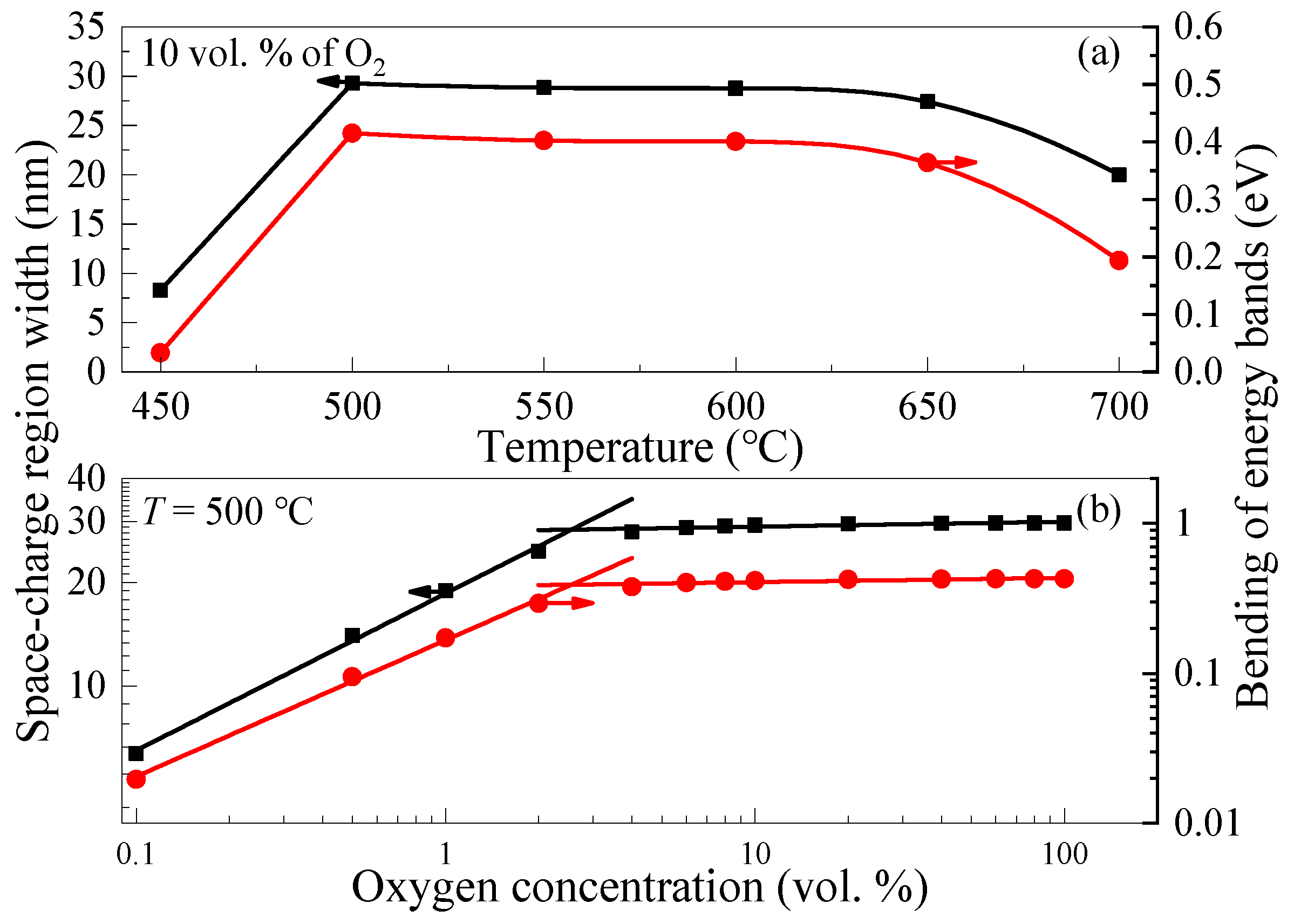
3.3. The Mechanism of the Sensory Effect

The ALD-deposited TiO2 thin films annealed at Tann = 800 °C in Ar for 30 min are corresponding to the anatase phase. They are homogeneous and relatively smooth, without features of microrelief on the film surface which could affect the transport of charge carriers through the film. Therefore, the increase in the resistance of such TiO2 films under exposure to oxygen is due to the chemisorption of O2 molecules on their surface. During chemisorption, oxygen captures electrons from the TiO2 conduction band and forms a region depleted by charge carriers in the near-surface part of the semiconductor film, with a width W. There are no charge carriers in this region, and the electric current between the contacts flows through a layer of thickness (dW), which is called a conduction channel. The negative charge on the surface of the n-type semiconductor film leads to the formation of the upward bending of energy band eVs, where vs. is the surface potential; e is the electron charge. It is shown that eVs~Ni2 [43,44], where Ni is the surface density of chemisorbed oxygen ions. The relationship between W and eVs has the following form:
W = LD × [2eVs/(kT)]0.5,
where LD = [(εε0kT/(e2n)]0.5; k is the Boltzmann constant; ε is the electric constant. The chemisorption of oxygen on the surface of TiO2 thin films leads to an increase in W and eVs, as well as to a decrease in the thickness of the conduction channel that leads to an increase in the resistance of the film. At n ≈ 1018 cm−3, LD for the anatase TiO2 phase increases linearly from 8.0 nm to 9.3 nm and does not exceed the film thickness. The TiO2 film resistance in gas mixture N2 + O2 is given by
RO = ρNl[b(dW)],
where ρN is the resistivity of the TiO2 film in the dry N2 atmosphere; l is the distance between the electrodes; b is the width of the TiO2 film. The intrinsic surface states can be neglected for ionic semiconductors [43]. Thus, in the N2 atmosphere, eVs and W = 0, and RN = ρNl/(bd). The expression for response to oxygen is
Sox = (1 − W/d)−1.
High Sox takes place when the region depleted by charge carriers extends almost the entire thickness of the film, but there is a very thin conduction channel. The dependences of W and eVs on T and cox (Figure 11a,b) are estimated by means of experimental Sox and calculated LD values. Pure TiO2 thin films do not demonstrate reliably recorded sensitivity to O2 at T < 450 °C. An increase in T stimulates dissociative adsorption of O2 molecules. At the same time, high W and eVs are observed in the range of T = 500–650 °C, indicating a high surface density of chemisorbed O ions. A further increase in T leads to a predominance of O desorption, which leads to a sharp decrease in W and eVs, as well as the response of films. There are two linear areas on the dependencies of W and eVs on the O2 concentration in double logarithmic coordinates (Figure 11b). eVs~coxl1 and W~coxm1 in the range of cox = 0.1–2 vol. %, where l1 and m1 are the power indexes. l1 = 0.90 ± 0.03 and m1 = 0.45 ± 0.01. The equality m1 = l1/2 follows from Expression (4). There are weaker power dependencies of eVs~coxl2 and W~coxm2 in the range of cox = 4–100 vol. %, where l2 and m2 are the power indexes. At the same time, l2 = 0.028 ± 0.006 and m2 = 0.014 ± 0.003. We assume that the manifestation of two linear areas on the dependencies is due to the presence of two types of adsorption centers for oxygen molecules. The possibility of this was shown for SnO2 and Ga2O3 thin films [45,46]. As a result, oxygen is chemisorbed in the form of O2− on the first type of adsorption centers and in the form of O on the second one. Chemisorption on the centers of the first type prevails in the range of cox = 0.1–2 vol. %. Twice as many electrons are captured during the chemisorption of one oxygen molecule on this type of centers, which causes a sharp increase in W and eVs. Centers of the second type prevail in the range of cox = 4–100 vol. % and the dependencies of W and eVs on cox are much weaker. In this case, eVs~(Ni1 + Ni2)2, where Ni1 is the surface density of chemisorbed O2− ions; Ni2 is the surface density of chemisorbed O ions. It is worth noting that it is possible to approximate the experimental dependence of the response on the O2 concentration (see Figure 8c) by means of Expressions (4) and (6) in the case when eVs(cox) = a(cox) × coxl1,2, where a is a function of cox. We believe that this dependence of eVs(cox) is due to the manifestation of the dependence of the surface density of adsorption centers for oxygen molecules on cox.
The effect of applied voltage on the response of metal oxide to gases has been poorly studied in the literature so far. For SnO2 films, it is shown that negatively charged ions of chemisorbed oxygen diffuse over the surface, participating in the transport of the electric current [47]. The diffusion time of adsorbed oxygen over the surface is less than its lifetime on the surface at high electric fields. Negatively charged ions accumulate near the anode and form a high-resistance region at higher electric fields. An additional increase in the resistance contributes to an increase in response at higher U.
Within the framework of the proposed mechanism of the sensory effect, the sensitivity of the films to reducing gases is due to the interaction of their molecules with previously chemisorbed oxygen, as a result of which W and eVs, as well as the resistance of TiO2 films, decrease. The mechanism of sensitivity of TiO2 films to reducing gases was previously described in detail by our group in ref. [48]. Oxidizing gases interact with the surface of TiO2 films like oxygen.
The proposed sensory effect does not take into account the contribution of changes in the potential barrier at the Pt/TiO2 interface under the exposure to gases. The Schottky barrier between a semiconductor and catalytically active metals such as Pt, Pd, Ru, Ir, and Ag, including Pt/TiO2 structures, are known to exhibit sensitivity to H2 and other gases [38,49,50]. According to the corresponding sensory effect’s mechanism, gas molecules (H2 for example) undergo a dissociative adsorption on the catalytically active metal surface. Then, H atoms diffuse through the metal layer to the metal–semiconductor interface. A dipole layer of H atoms is formed at this interface, which leads to a decrease in the height of a potential barrier for electrons at the metal–semiconductor interface and an increase in the current. The diffusion of H atoms in Pt is characterized by lower diffusion activation energies and higher diffusion coefficients than those for the diffusion of O atoms in Pt [51,52,53,54,55,56]. It can be estimated that the diffusion times of H atoms through a 330 nm thick Pt layer are less than 0.055 s. In contrast, the diffusion time of O atoms through the Pt contact layer is about 108 s. Thus, changes in the potential barrier at the Pt/TiO2 interface under the exposure to O2 should not be taken into account. However, this effect may be the main one under the exposure to other gases, such as H2 and CO.
The gas-sensitive characteristics of TiO2 films synthesized by different deposition methods under the exposure to O2 are compared in Table 2, where NRA is nanorod array; NPs is the nanoparticles; NFs are the nanoflakelets; NTs is the nanotubes; RFMS is the radio frequency magnetron sputtering; DCMS is the direct current magnetron sputtering; IBSD is the ion beam sputtering deposition; GLAD + EBE is the glancing angle deposition with electron beam evaporation; AVO is the acid vapor oxidation; USP is the ultrasonic spray pyrolysis; TD + HM is the thermal decomposition assisted hydrothermal method; PEO is the plasma electrolytic oxidation; AO is the anodic oxidation; UV is the exposure to ultraviolet radiation. The gas-sensitive properties of ALD-deposited undoped TiO2 thin films studied in this work are comparable or superior to the results reported for undoped TiO2 thin films grown by other methods. High Sox requires heating of the structures to T > 300 °C. T is reduced to RT by using of the ultrathin films or nanostructures, exposure to UV. However, at the same time, tres and trec significantly increase. On the other hand, an increase in Sox is achieved by doping of TiO2 with Nb, Pd and Cr, introducing ZrO2, MoO3, forming of multilayer structures, and modifying the surface of films with nanoparticles.

4. Conclusions

The structural and gas-sensitive properties under the exposure to O2 within the temperature range from 30 °C to 700 °C of TiO2 thin films deposited by atomic layer deposition on SiO2/Si substrates were studied. The structure of the films annealed at 800 °C in an Ar for 30 min corresponded to the anatase phase. They are homogeneous and relatively smooth. The ALD-TiO2 thin films demonstrated high responses to O2 in the dynamic range from 0.1 to 100 vol. % and to low concentrations of H2, NO2. The greatest response—41.5 arb. un.—was observed at a temperature of 500 °C under exposure to 10 vol. % of O2. A mechanism describing the sensory effect in the ALD-TiO2 thin films was proposed. The resistance of the films increases due to the chemisorption of oxygen molecules on their surface that decreases the thickness of the conduction channel between the metal contacts. It was suggested that there are two types of adsorption centers on the TiO2 thin films surface: oxygen is chemisorbed in the form of O2– on the first one and O on the second one.

Author Contributions

Conceptualization, A.V.A. and M.G.V.; methodology, N.N.Y., G.A.R. and K.I.L.; software, N.N.Y., G.A.R. and K.I.L.; validation, A.V.A.; formal analysis, A.V.A., M.G.V., G.A.R. and K.I.L.; investigation, N.N.Y., D.A.A., G.A.R. and K.I.L.; resources, A.V.A. and M.G.V.; data curation, A.V.A., D.A.A., M.G.V., G.A.R. and K.I.L.; writing—original draft preparation, A.V.A., D.A.A., M.G.V., G.A.R. and K.I.L.; writing—review and editing, A.V.A., D.A.A., M.G.V., G.A.R. and K.I.L.; visualization, A.V.A., M.G.V., G.A.R. and K.I.L.; supervision, A.V.A. and M.G.V.; project administration, A.V.A. and M.G.V.; funding acquisition, A.V.A. All authors have read and agreed to the published version of the manuscript.

Funding

Researches of gas-sensing properties of the ALD-deposited TiO2 thin films were supported by the Russian Science Foundation, grant number 20-79-10043-P.

Data Availability Statement

Not applicable.

Conflicts of Interest

The authors declare no conflict of interest.

References

  1. Kong, X.-H.; Wang, X.-F.; Liu, Q.-G. Research on oxygen sensor for metallurgical process. J. Iron Steel Res. Int. 2001, 8, 60–62. [Google Scholar]
  2. Lampe, U.; Fleischer, M.; Meixner, H. Lambda measurement with Ga2O3. Sens. Actuators B Chem. 1994, 17, 187–196. [Google Scholar] [CrossRef]
  3. Ramamoorthy, R.; Dutta, P.K.; Akbar, S.A. Oxygen sensors: Materials, methods, designs and applications. J. Mater. Sci. 2003, 38, 4271–4282. [Google Scholar] [CrossRef]
  4. Jyothilal, H.; Shukla, G.; Walia, S.; Bharath, S.P.; Angappane, S. UV assisted room temperature oxygen sensors using titanium dioxide nanostructures. Mater. Res. Bull. 2021, 140, 111324. [Google Scholar] [CrossRef]
  5. Wang, Y.; Lai, X.; Liu, B.; Chen, Y.; Lu, Y.; Wang, F.; Zhang, L. UV-induced desorption of oxygen at the TiO2 surface for highly sensitive room temperature O2 sensing. J. Alloys Compd. 2019, 793, 583–589. [Google Scholar] [CrossRef]
  6. Gan, L.; Wu, C.; Tan, Y.; Chi, B.; Pu, J.; Jian, L. Oxygen sensing performance of Nb-doped TiO2 thin film with porous structure. J. Alloys Compd. 2014, 585, 729–733. [Google Scholar] [CrossRef]
  7. Polyakov, A.Y.; Smirnov, N.B.; Shchemerov, I.V.; Yakimov, E.B.; Pearton, S.J.; Ren, F.; Chernykh, A.V.; Gogova, D.; Kochkova, A.I. Electrical properties, deep trap and luminescence spectra in semi-insulating, Czochralski β-Ga2O3 (Mg). ECS J. Solid State Sci. Technol. 2019, 8, Q3019. [Google Scholar] [CrossRef]
  8. Dimitrova, Z.; Gogova, D. On the structure, stress and optical properties of CVD tungsten oxide films. Mater. Res. Bull. 2005, 40, 333–340. [Google Scholar] [CrossRef]
  9. Gogova, D.; Gesheva, K.; Kakanakova-Georgieva, A.; Surtchev, M. Investigation of the structure of tungsten oxide films obtained by chemical vapor deposition. Eur. Phys. J. Appl. Phys. 2000, 11, 167–174. [Google Scholar] [CrossRef]
  10. Gogova, D.; Iossifova, A.; Ivanova, T.; Dimitrova, Z.; Gesheva, K. Electrochromic behavior in CVD grown tungsten oxide films. J. Cryst. Growth 1999, 198–199, 1230–1234. [Google Scholar] [CrossRef]
  11. Kachel, K.; Korytov, M.; Gogova, D.; Galazka, Z.; Albrecht, M.; Zwierz, R.; Siche, D.; Golka, S.; Kwasniewski, A.; Schmidbauer, M.; et al. A new approach to free-standing GaN using β-Ga2O3 as a substrate. CrystEngComm 2012, 14, 8536–8540. [Google Scholar] [CrossRef]
  12. Stolze, M.; Gogova, D.; Thomas, L.-K. Analogy for the maximum obtainable colouration between electrochromic, gaschromic, and electrocolouration in DC-sputtered thin WO3−y films. Thin Solid Films 2005, 476, 185–189. [Google Scholar] [CrossRef]
  13. Nikolskaya, A.; Okulich, E.; Korolev, D.; Stepanov, A.; Nikolichev, D.; Mikhaylov, A.; Tetelbaum, D.; Almaev, A.; Bolzan, C.A.; Buaczik, A., Jr.; et al. Ion implantation in β-Ga2O3: Physics and technology. J. Vac. Sci. Technol. A 2021, 39, 030802. [Google Scholar] [CrossRef]
  14. Zappa, D.; Galstyan, V.; Kaur, N.; Hashitha, M.M.; Sisman, O.; Comini, E. Metal oxide -based heterostructures for gas sensors. Anal. Chim. Acta 2018, 1039, 1–23. [Google Scholar] [CrossRef]
  15. Yakovlev, N.N.; Almaev, A.V.; Nikolaev, V.I.; Kushnarev, B.O.; Pechnikov, A.I.; Stepanov, S.I.; Chikiryaka, A.V.; Timashov, R.B.; Scheglov, M.P.; Butenko, P.N.; et al. Low-resistivity gas sensors based on the In2O3-Ga2O3 mixed compounds films. Mater. Today Commun. 2023, 34, 105241. [Google Scholar] [CrossRef]
  16. Zhu, J.; Xu, Z.; Ha, S.; Li, D.; Zhang, K.; Zhang, H.; Feng, J. Gallium oxide for gas sensor applications: A comprehensive review. Materials 2022, 15, 7339. [Google Scholar] [CrossRef]
  17. Mokrushin, A.S.; Simonenko, E.P.; Simonenko, N.P.; Bukunov, K.A.; Gorobtsov, P.Y.; Sevastyanov, V.G.; Kuznetsov, N.T. Gas-sensing properties of nanostructured TiO2–xZrO2 thin films obtained by the sol–gel method. J. Sol.-Gel. Sci. Technol. 2019, 92, 415–426. [Google Scholar] [CrossRef]
  18. Lu, C.; Huang, Y.; Huang, J.; Chang, C.; Wu, S. A Macroporous TiO2 oxygen sensor fabricated using anodic aluminium oxide as an etching mask. Sensors 2010, 10, 670–683. [Google Scholar] [CrossRef]
  19. Wang, H.; Chen, L.; Wang, J.; Sun, Q.; Zhao, Y. A micro oxygen sensor based on a nano sol-gel TiO2 thin film. Sensors 2014, 14, 16423–16433. [Google Scholar] [CrossRef]
  20. Wang, H.; Sun, Q.; Yao, Y.; Li, Y.; Wang, J.; Chen, L. A micro sensor based on TiO2 nanorod arrays for the detection of oxygen at room temperature. Ceram. Int. 2016, 42, 8565–8571. [Google Scholar] [CrossRef]
  21. Wilson, R.L.; Simion, C.E.; Blackman, C.S.; Carmalt, C.J.; Stanoiu, A.; Di Maggio, F.; Covington, J.A. The effect of film thickness on the gas sensing properties of ultra-thin TiO2 films deposited by atomic layer deposition. Sensors 2018, 18, 735. [Google Scholar] [CrossRef] [PubMed]
  22. Du, X.; George, S.M. Thickness dependence of sensor response for CO gas sensing by tin oxide films grown using atomic layer deposition. Sens. Actuators B Chem. 2008, 135, 152–160. [Google Scholar] [CrossRef]
  23. Marichy, C.; Donato, N.; Latino, M.; Willinger, M.G.; Tessonnier, J.-P.; Neri, G.; Pinna, N. Gas sensing properties and p-type response of ALD TiO2 coated carbon nanotubes. Nanotechnology 2015, 26, 024004. [Google Scholar] [CrossRef] [PubMed]
  24. Niskanen, A.J.; Varpula, A.; Utriainen, M.; Natarajan, G.; Cameron, D.C.; Novikov, S.; Airaksinen, V.-M.; Sinkkonen, J.; Franssila, S. Atomic layer deposition of tin dioxide sensing film in microhotplate gas sensors. Sens. Actuators B Chem. 2010, 148, 227–232. [Google Scholar] [CrossRef]
  25. Rosental, A.; Tarre, A.; Gerst, A.; Sundqvist, J.; Hårsta, A.; Aidla, A.; Aarik, J.; Sammelselg, V.; Uustare, T. Gas sensing properties of epitaxial SnO2 thin films prepared by atomic layer deposition. Sens. Actuators B Chem. 2003, 93, 552–555. [Google Scholar] [CrossRef]
  26. Wei, Z.; Akbari, M.K.; Hai, Z.; Ramachandran, R.K.; Detavernier, C.; Verpoort, F.; Kats, E.; Xu, H.; Hu, J.; Zhuiykov, S. Ultra-thin sub-10 nm Ga2O3-WO3 heterostructures developed by atomic layer deposition for sensitive and selective C2H5OH detection on ppm level. Sens. Actuators B Chem. 2019, 287, 147–156. [Google Scholar] [CrossRef]
  27. Kim, D.H.; Kim, W.-S.; Lee, S.B.; Hong, S.-H. Gas sensing properties in epitaxial SnO2 films grown on TiO2 single crystals with various orientations. Sens. Actuators B Chem. 2010, 147, 653–659. [Google Scholar] [CrossRef]
  28. Lee, J.-H.; Mirzaei, A.; Kim, J.-H.; Kim, J.-Y.; Nasriddinov, A.F.; Rumyantseva, M.N.; Kim, H.W.; Kim, S.S. Gas-sensing behaviors of TiO2-layer-modified SnO2 quantum dots in self-heating mode and effects of the TiO2 layer. Sens. Actuators B Chem. 2020, 310, 127870. [Google Scholar] [CrossRef]
  29. Xu, H.; Akbari, M.K.; Wei, Z.; Hu, J.; Verpoort, F.; Zhuiykov, S. Plasma-induced sub-10 nm Au-SnO2-In2O3 heterostructures fabricated by atomic layer deposition for highly sensitive ethanol detection on ppm level. Appl. Surf. Sci. 2021, 563, 150400. [Google Scholar] [CrossRef]
  30. Eadi, S.B.; Shin, H.J.; Song, K.W.; Choi, H.W.; Kim, S.H.; Lee, H.D. Development of ultrasensitive indium oxide layer with high response to NO2 gas in indium gallium zinc oxide stack structure using atomic layer deposition. Mater. Lett. 2021, 297, 129943. [Google Scholar] [CrossRef]
  31. Lou, C.; Yang, C.; Zheng, W.; Liu, X.; Zhang, J. Atomic layer deposition of ZnO on SnO2 nanospheres for enhanced formaldehyde detection. Sens. Actuators B Chem. 2021, 329, 129218. [Google Scholar] [CrossRef]
  32. Lou, C.; Huang, Q.; Li, Z.; Lei, G.; Liu, X.; Zhang, J. Fe2O3-sensitized SnO2 nanosheets via atomic layer deposition for sensitive formaldehyde detection. Sens. Actuators B Chem. 2021, 345, 130429. [Google Scholar] [CrossRef]
  33. Yeh, Y.-M.; Chang, S.-J.; Wang, P.-H.; Hsueh, T.-J. A TSV-structured room temperature p-Type TiO2 nitric oxide gas sensor. Appl. Sci. 2022, 12, 9946. [Google Scholar] [CrossRef]
  34. Kuo, C.-G.; Chen, J.-H.; Chao, Y.-C.; Chen, P.-L. Fabrication of a P3HT-ZnO nanowires gas sensor detecting ammonia gas. Sensors 2018, 18, 37. [Google Scholar] [CrossRef]
  35. Bukauskas, V.; Olekas, A.; Senulien, D.; Strazdien, V.; Šetkus, A.; Kaciulis, S.; Pandolfi, L. Effect of thickness of ultra-thin tin oxide film based gas sensors. Lith. J. Phys. 2007, 47, 475–483. [Google Scholar] [CrossRef]
  36. Kozhushner, M.A.; Bodneva, V.L.; Trakhtenberg, L.I. Sensor effect theory for the detection of reducing gases. Rus. J. Phys. Chem. A 2012, 86, 1281–1287. [Google Scholar] [CrossRef]
  37. Ikim, M.I.; Gromov, V.F.; Gerasimov, G.N.; Spiridonova, E.Y.; Erofeeva, A.R.; Kurmangaleev, K.S.; Polunin, K.S.; Ilegbusi, O.J.; Trakhtenberg, L.I. Structure, conductivity, and sensor properties of nanosized ZnO-In2O3 composites: Influence of synthesis method. Micromachines 2023, 14, 1685. [Google Scholar] [CrossRef]
  38. Almaev, A.V.; Nikolaev, V.I.; Yakovlev, N.N.; Butenko, P.N.; Stepanov, S.I.; Pechnikov, A.I.; Scheglov, M.P.; Chernikov, E.V. Hydrogen sensors based on Pt/α-Ga2O3:Sn/Pt structures. Sens. Actuators B Chem. 2022, 364, 131904. [Google Scholar] [CrossRef]
  39. Bulyarskiy, S.; Koiva, D.; Gusarov, S.; Latipov, E.; Rudakov, G.; Svetukhin, V. Crystallization of amorphous titanium oxide films upon annealing in an oxygen atmosphere. Mater. Sci. Eng. B 2022, 283, 115802. [Google Scholar] [CrossRef]
  40. Maksimova, N.K.; Almaev, A.V.; Sevastyanov, E.Y.; Potekaev, A.I.; Chernikov, E.V.; Sergeychenko, N.V.; Korusenko, P.M.; Nesov, S.N. Effect of additives Ag and rare-earth elements Y and Sc on the properties of hydrogen sensors based on thin SnO2 films during long-term testing. Coatings 2019, 9, 423. [Google Scholar] [CrossRef]
  41. Meixner, H.; Lampe, U.; Gerblinger, J.; Fleischer, M. Chemosensors for motor management systems of the future. Fresenius’ J. Anal. Chem. 1994, 348, 536–541. [Google Scholar] [CrossRef]
  42. Baranzahi, A.; Spetz, A.L.; Glavmo, M.; Carlsson, C.; Nytomt, J.; Salomonsson, P.; Jobson, E.; Häggendal, B.; Mårtensson, P.; Lundström, I. Response of metal-oxide-silicon carbide sensors to simulated and real exhaust gases. Sens. Actuators B Chem. 1997, 43, 52–59. [Google Scholar] [CrossRef]
  43. Gaman, V.I. Physical principles of operation of oxidizing gas sensors based on metal oxide semiconductors. Rus. Phys. J. 2012, 54, 1364–1371. [Google Scholar] [CrossRef]
  44. Simion, C.E.; Schipani, F.; Papadogianni, A.; Stanoiu, A.; Budde, M.; Oprea, A.; Weimar, U.; Bierwagen, O.; Barsan, N. Conductance model for single-crystalline/compact metal oxide gas-sensing layers in the nondegenerate limit: Example of epitaxial SnO2(101). ACS Sens. 2019, 4, 2420–2428. [Google Scholar] [CrossRef] [PubMed]
  45. Gaman, V.I.; Almaev, A.V.; Sevast’yanov, E.Y.; Maksimova, N.K. Influence of water vapors and hydrogen on the energy band bending in the SnO2 microcrystals of polycrystalline tin dioxide films. Rus. Phys. J. 2015, 58, 179–187. [Google Scholar] [CrossRef]
  46. Almaev, A.V.; Chernikov, E.V.; Novikov, V.V.; Kushnarev, B.O.; Yakovlev, N.N.; Chuprakova, E.V.; Oleinik, V.L.; Lozinskaya, A.D.; Gogova, D.S. Impact of Cr2O3 additives on the gas-sensitive properties of β-Ga2O3 thin films to oxygen, hydrogen, carbon monoxide, and toluene vapors. J. Vac. Sci. Technol. A 2021, 39, 023405. [Google Scholar] [CrossRef]
  47. Simakov, V.V.; Yakusheva, O.V.; Grebennikov, A.I.; Kisin, V.V. Current-voltage characteristics of thin-film gas sensor structures based on tin dioxide. Tech. Phys. Lett. 2005, 31, 339. [Google Scholar] [CrossRef]
  48. Almaev, A.V.; Yakovlev, N.N.; Kushnarev, B.O.; Kopyev, V.V.; Novikov, V.A.; Zinoviev, M.M.; Yudin, N.N.; Podzivalov, S.N.; Erzakova, N.N.; Chikiryaka, A.V.; et al. Gas sensitivity of IBSD deposited TiO2 Thin Films. Coatings 2022, 12, 1565. [Google Scholar] [CrossRef]
  49. Kwon, H.; Lee, Y.; Hwang, S.; Kim, J.K. Highly-sensitive H2 sensor operating at room temperature using Pt/TiO2 nanoscale Schottky contacts. Sens. Actuators B Chem. 2017, 241, 985–992. [Google Scholar] [CrossRef]
  50. Schierbaum, K.D.; Kirner, U.K.; Geiger, J.F.; Göpel, W. Schottky-barrier and conductivity gas sensors based upon Pd/SnO2 and Pt/TiO2. Sens. Actuators B Chem. 1991, 4, 87–94. [Google Scholar] [CrossRef]
  51. Ebisuzaki, Y.; Kass, W.J.; O’Keeffe, M. Solubility and diffusion of hydrogen and deuterium in platinum. J. Chem. Phys. 1968, 49, 3329–3332. [Google Scholar] [CrossRef]
  52. Ishikawa, T.; McLellan, R.B. The diffusivity of hydrogen in the noble metals at low temperature. Acta Metall. 1985, 33, 1979–1985. [Google Scholar] [CrossRef]
  53. Ferrin, P.; Kandoi, S.; Nilekar, A.; Mavrikakis, M. Hydrogen adsorption, absorption and diffusion on and in transition metal surfaces: A DFT study. Surf. Sci. 2012, 606, 679–689. [Google Scholar] [CrossRef]
  54. Barth, J. Transport of adsorbates at metal surfaces: From thermal migration to hot precursors. Surf. Sci. Rep. 2000, 40, 75–149. [Google Scholar] [CrossRef]
  55. Schmiedl, R.; Demuth, V.; Lahnor, P.; Godehardt, H.; Bodschwinna, Y.; Harder, C.; Hammer, L.; Strunk, H.; Schulz, M.; Heinz, K. Oxygen diffusion through thin Pt films on Si(100). Appl. Phys. A 1996, 62, 223–230. [Google Scholar] [CrossRef]
  56. Velho, L.; Bartlett, R. Diffusivity and solubility of oxygen in platinum and Pt-Ni alloys. Metall. Trans. 1972, 3, 65–72. [Google Scholar] [CrossRef]
  57. Castañeda, L.; López-Suárez, A.; Tiburcio-Silver, A. Influence of colloidal silver nanoparticles on the novel flower-like titanium dioxide oxygen sensor performances. J. Nanosci. Nanotechnol. 2010, 10, 1343–1348. [Google Scholar] [CrossRef]
  58. Galatsis, K.; Li, Y.X.; Wlodarski, W.; Comini, E.; Faglia, G.; Sberveglieri, G. Semiconductor MoO3–TiO2 thin film gas sensors. Sens. Actuators B Chem. 2001, 77, 472–477. [Google Scholar] [CrossRef]
  59. Jiao, M.; Zhao, X.; He, X.; Wang, G.; Zhang, W.; Rong, Q.; Nguyen, D. High-performance MEMS oxygen sensors based on Au/TiO2 films. Chemosensors 2023, 11, 476. [Google Scholar] [CrossRef]
  60. Raghu, A.V.; Karuppanan, K.K.; Pullithadathil, B. Highly Sensitive, Temperature-independent oxygen gas sensor based on anatase TiO2 nanoparticle grafted, 2D mixed valent VOx nanoflakelets. ACS Sens. 2018, 3, 1811–1821. [Google Scholar] [CrossRef]
  61. Engelkamp, B.; Schierbaum, K. Oxygen sensing of Pt/PEO-TiO2 in humid atmospheres at moderate temperatures. Sensors 2021, 21, 2558. [Google Scholar] [CrossRef] [PubMed]
  62. Lu, H.F.; Li, F.; Liu, G.; Chen, Z.G.; Wang, D.W.; Fang, H.T.; Lu, G.Q.; Jiang, Z.H.; Cheng, H.M. Amorphous TiO2 nanotube arrays for low-temperature oxygen sensors. Nanotechnology 2008, 19, 405504. [Google Scholar] [CrossRef] [PubMed]
  63. Wang, H.; Wang, J.; Chen, L.; Yao, Y.; Sun, Q.; Qunming, Z. Integrated microoxygen sensor based on nanostructured TiO2 thin films. Micro Nano Lett. 2015, 10, 597–602. [Google Scholar] [CrossRef]
Figure 1. Microscopic photo of the sample based on TiO2 thin film.
Micromachines 14 01875 g001
Figure 2. XRD patterns of the ALD-TiO2 thin films.
Micromachines 14 01875 g002
Figure 3. AFM images of annealed ALD-TiO2 thin film surface.
Micromachines 14 01875 g003
Figure 4. BF-TEM cross-sectional image of annealed ALD-TiO2 thin film on SiO2/Si substrate, the insertion is the diffraction pattern.
Micromachines 14 01875 g004
Figure 5. (a) Elementwise TEM-EDX mapping of cross-section of annealed ALD-TiO2 thin film; (b) EDX spectrum of annealed ALD-TiO2 thin film.
Micromachines 14 01875 g005
Figure 6. (a) Temperature dependences of response to 10 vol. % and 40 vol. % of O2; (b) Temperature dependences of response and recovery times upon exposure to 10 vol. % of O2.
Micromachines 14 01875 g006
Figure 7. Time dependence of resistance upon cyclic exposure to 10 vol. % of O2 at T = 500 °C for new sample (a) and after 4 weeks of storing (b).
Micromachines 14 01875 g007
Figure 8. (a) Time dependence of resistance under stepwise increase in the O2 concentration at T = 500 °C; (b) Time profile of O2 concentration changes; (c) dependence of response on O2 concentration in dynamic range from 0.1 vol. % to 100 vol. % of O2 at T = 500 °C; (d) dependence of response on O2 concentration in dynamic range from 0.1 vol. % to 6 vol. % of O2 at T = 500 °C.
Micromachines 14 01875 g008
Figure 9. (a) IV characteristics in N2 atmosphere and gas mixture of N2 + 10 vol. of O2 at T = 500 °C; (b) dependencies of the responses to 10 vol. % of O2 on applied voltage at T = 500 °C.
Micromachines 14 01875 g009
Figure 10. Responses to fixed concentrations of O2, H2, CO, CH4, CO2, NO2 and NO at T = 500 °C.
Micromachines 14 01875 g010
Figure 11. (a) Dependences of space-charge region width and bending of energy bands on temperature at cox = 10 vol. % of O2; (b) dependences of space-charge region width and bending of energy bands on oxygen concentration at T = 500 °C.
Micromachines 14 01875 g011
Table 1. Comparison of gas-sensitive characteristics of ALD-deposited metal oxide thin films.
Materiald (nm)Gascg (ppm)T (°C)S (arb. un.)Ref.
TiO250NH31003504.24[21]
CNT/TiO210 (TiO2)NO28150~10[23]
SnO217.5C2H5OH5003001.64[24]
SnO210CO104450~21[25]
WO36.5C2H5OH100275~14[26]
Ga2O31.5~1.4
Ga2O3/WO31.5/6.5~3.5
SnO290H21000400~380[27]
TiO2/SnO2 QDs30 (TiO2)CO13001.8[28]
SnO24.4C2H5OH20040020[29]
In2O3/SnO24/4.435037
IGZO150NO21002005154[30]
ZnO/SnO2 NSs24 (ZnO)HCHO2020038.2[31]
Fe2O3/SnO2 NShs20 cyclesHCHO202204.57[32]
p-TiO270NO10RT1.244[33]
P3HT/ZnO NWs-NH35RT1.35[34]
Table 2. Comparison of sensitivity to O2 for TiO2 thin films deposited by different methods.
MaterialMethodsd (nm)cox (vol. %)T (°C)Sox (arb. un.)Ref.
TiO2RFMS500.65001.14[18]
TiO2DCMS6010RT76[5]
TiO2IBSD130407507.64[48]
TiO2sol-gel-27006.5[6]
Nb (6%):TiO2-73.2
TiO2sol-gel-14004.4[17]
TiO2 + ZrO2 (10 mol. %)-5
TiO2RFMS3010RT + UV~5.5[4]
Cr-TiO2/TiO2GLAD + EBE-~9
TiO2 NRAAVO-8RT~1.9[20]
TiO2USP-0.13005[57]
TiO2-Ag NPs-9
Pd:TiO2sol-gel~1101→202401.27[19]
TiO2sol-gel-0.142028[58]
TiO2 + MoO3 (25 at. %)37030
Au (6 nm)/TiO2RFMS300540061.3[59]
VOx/TiO2 NFsTD + HM-0.015001.32[60]
Pt/TiO2PEO-10RT2[61]
TiO2 NTsAO-4100160[62]
TiO2sol-gel-42521.16[63]
TiO2ALD230.15001.27This work
12.70
25.55
1041.61
Disclaimer/Publisher’s Note: The statements, opinions and data contained in all publications are solely those of the individual author(s) and contributor(s) and not of MDPI and/or the editor(s). MDPI and/or the editor(s) disclaim responsibility for any injury to people or property resulting from any ideas, methods, instructions or products referred to in the content.

