Abstract
SiC/Si and GaN/Si heterojunction technology has been widely used in power semiconductor devices, and SiC/Si VDMOS and GaN/Si VDMOS were proposed in our previous paper. Based on existing research, breakdown point transfer technology (BPT) was used to optimize SiC/Si VDMOS. Simulation results showed that the BV of the SiC/Si heterojunction VDMOS was considerably increased from 259 V to 1144 V, and Ron,sp decreased from 18.2 mΩ·cm2 to 6.03 mΩ·cm2 compared with Si VDMOS. In order to analyze the characteristics of the SiC/Si heterojunction structure deeply, the influence of the interface state characteristics of the SiC/Si heterojunction on the electrical parameters of VDMOS was analyzed, including electric field characteristics, blocking characteristics, output characteristics, and transfer characteristics. In addition, the influence of the interface state of the SiC/Si heterojunction on energy band characteristics was analyzed. The results showed that with an increase in the interfacial charge (acceptor) concentration, the p-type trap layer was introduced into the interface of the SiC/Si heterojunction, energy increased slightly, and the barrier height difference at the heterojunction increased, resulting in an increase in BV. At the same time, since the barrier height became higher, electrons did not flow easily, so Ron,sp increased. On the contrary, when a charge (donor) was introduced at the interface of the SiC/Si heterojunction, the number of electrons in the channel increased, resulting in an increase in the electron current, which is conducive to the flow of electrons, resulting in a decrease in Ron,sp. The energy band and other characteristics of devices with temperature were simulated at different temperatures. Finally, the effects of SiC/Si heterojunction interface states on interface capacitances and switching performances of VDMOS devices were also discussed.
1. Introduction
A vertical double-diffusion metal oxide semiconductor (VDMOS) is an important component in the field of power semiconductor devices; due to its fast switching speed, low loss, high input impedance, low driving power, and excellent frequency characteristics, it has been widely used in power integrated circuits and power integrated systems [1,2,3,4,5,6,7,8,9,10]. However, the main problem of VDMOS power devices is that the specific on-resistance (Ron,sp) of the device increases sharply with an increase in breakdown voltage (BV), which greatly limits the development and application of VDMOS power devices [11,12,13,14,15,16,17,18,19,20,21,22,23,24,25,26,27,28].
However, efforts to improve Si power devices are always limited by the low critical electric field of Si, which gives an opportunity for the development of SiC devices. SiC materials have a large bandgap and a critical electric field about 10 times that of Si, which can break the limit of Si materials [25,26,27,28,29,30,31,32,33,34,35,36,37,38,39,40,41,42,43,44,45,46,47]. Nevertheless, SiC power devices suffer from gate oxide reliability and some difficulties in manufacturing processes, such as the diffusion of impurity and the realization of high-quality ohm contact [16,17]. Moreover, manufacturing SiC devices is much more costly compared with Si devices. The successful fabrication of SiC/Si substrates offers a practical approach to solving these problems [18,19,20,21,22].
A SiC/Si heterojunction VDMOS combines the mature process of Si materials with the wide bandgap of SiC materials. Thus, a high critical breakdown electric field can optimize BV compared with a traditional Si-based power device [16,17]. The contradiction between BV and Ron,sp is optimized, and the high thermal conductivity of SiC materials is beneficial to the heat dissipation of a VDMOS device, which effectively improves the performance of the device. Since the active region of the device is formed from silicon semiconductor material, a mature silicon process can be employed in the device fabrication process to achieve better ohmic contact [16,17,18,19,20,21,22,23,24,25]. SiC/Si VDMOS and GaN/Si VDMOS were proposed in our previous paper, and the influence of device electrical and structural parameters was studied [16,18]. However, this paper mainly discusses the influence of the interface state on the electric field, band energy distribution, temperature, and switching characteristics.
2. Materials and Methods
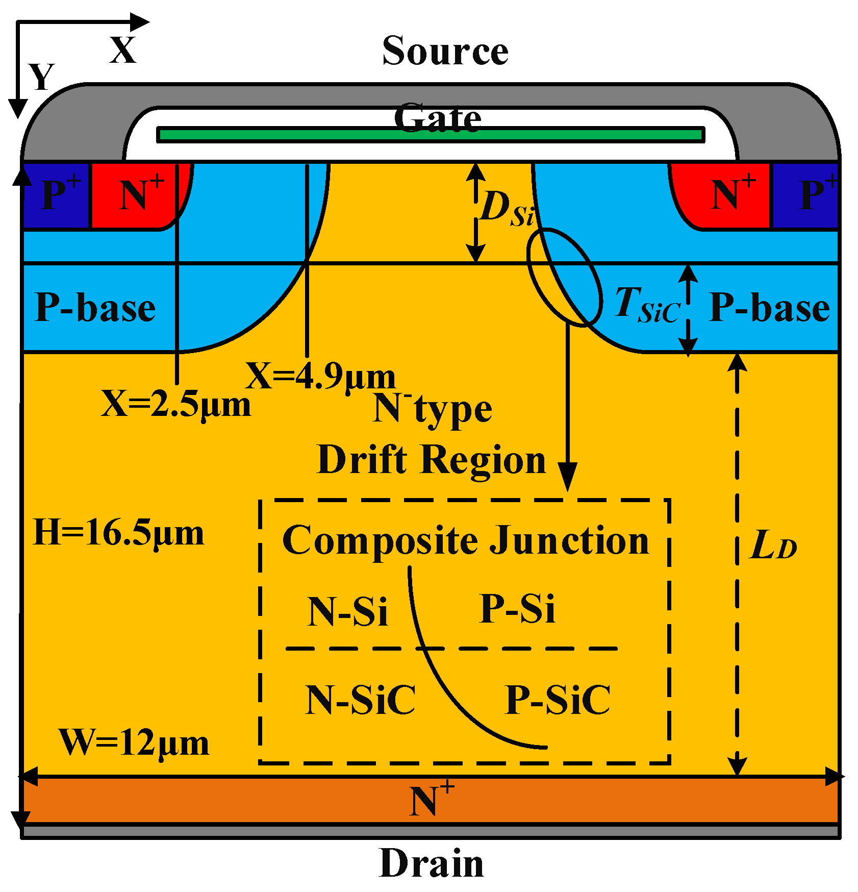
In this paper, a VDMOS with SiC/Si heterojunction was used to optimize BV by breakdown point transfer (BPT), which transfers the breakdown point from a high electric field to a low electric field. Figure 1 shows a cell of the proposed SiC/Si heterojunction VDMOS; the formation of the Si/SiC substrate can be realized by the method in [22]. “DSi” is defined as the Si thickness, “LD” is the length of N− drift region, and “ND” is the concentration of N− drift region in the structures.

Figure 1.
Cross-section of the novel SiC/Si VDMOS.
In this paper, a two-dimensional numerical simulation of SiC/Si VDMOS is performed using ISE-TCAD. The main physics models were applied in Synopsys SentaurusTM tools simulation, including Mobility (DopingDep High Field Sat Enormal), EffectiveIntrinsic Density (OldSlotboom), and Recombination (SRH (DopingDep) and Auger Avalanche (Eparal)). The criterion of breakdown was BreakCriteria {Current (Contact = “drain” Absval = 1 × 10⁻⁷)}. The main solving model was Coupled {Poisson Electron Hole}. For the coordinates, it was necessary to optimize the parameters in the numerical simulations. Some of the device parameters in the simulation are presented in Table 1. The ambient temperature was 300 K, the breakdown voltage (BV) was obtained at VGS = 0 V, and the specific on-resistance (Ron,sp) was obtained at VGS = 10 V; the simulation results of the four devices are shown in Table 2.

Table 1.
Device parameters in the simulation.
Table 2.
Simulation results for the Si VDMOS, SiC/Si VDMOS, SiC VDMOS, and GaN/Si VDMOS.
3. Results and Discussion
3.1. The Influence of Interface State on Electrical Parameters
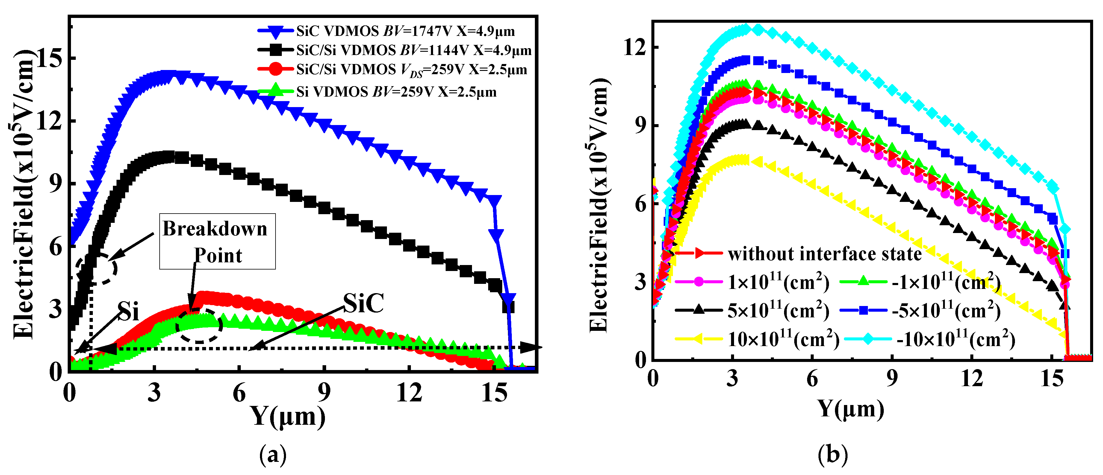
The vertical electric field for SiC/Si VDMOS, Si VDMOS, and SiC VDMOS are shown in Figure 2a. For SiC VDMOS, BV reached 1747V. For Si VDMOS, when X = 2.5 μm (shown in Figure 1), the maximum field strength was 3.03 × 10⁵ V/cm (reaching the critical breakdown electric field of Si materials), and BV was 259 V of Si VDMOS. For SiC/Si VDMOS, when the drain voltage reached 259 V, the electric field strength at the interface between the P-base and the N-type drift regions did not reach the critical breakdown field strength of SiC, so the device did not break down. As the drain voltage was further increased, the electric field strength of the device increased until the electric field at the heterojunction reached 3.45 × 10⁵ V/cm (reaching the critical breakdown field of the Si materials), and the SiC/Si VDMOS broke down. Therefore, the BV of SiC/Si VDMOS was increased from 259 V to 1144 V compared with the conventional Si VDMOS [16,17]. According to previous experimental results [23,24], SiC/Si interfacial charges were introduced during the direct bonding process. The effect of different interface state charge concentrations on the vertical electric field of SiC/Si VDMOS is shown in Figure 2b. The type of interface state charge introduced was donor (electron) or acceptor (hole) in this paper. An increase in the interface state charge (acceptorlike) concentrations resulted in an increase in the vertical electric field of the SiC/Si VDMOS compared with SiC/Si VDMOS without an interface state charge. This is because of the p-type trap layer introduced by the interface charge (acceptor) at the SiC/Si heterojunction, which enhanced the internal electric field at the SiC/Si interface and changed the distribution of the electric field. As the interface state charge (donor) concentration increased, the vertical electric field at the SiC/Si heterojunction decreased.
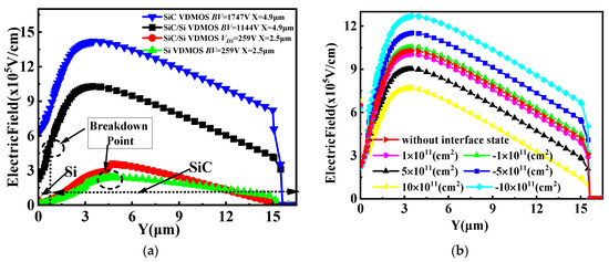
Figure 2.
(a) Vertical electric field distributions for SiC/Si VDMOS, Si VDMOS, and SiC VDMOS, and (b) the influence of different interface state charges (acceptorlike and donor) on the vertical electric field of SiC/Si VDMOS: LD = 5 μm, DSi = 0.5 μm.
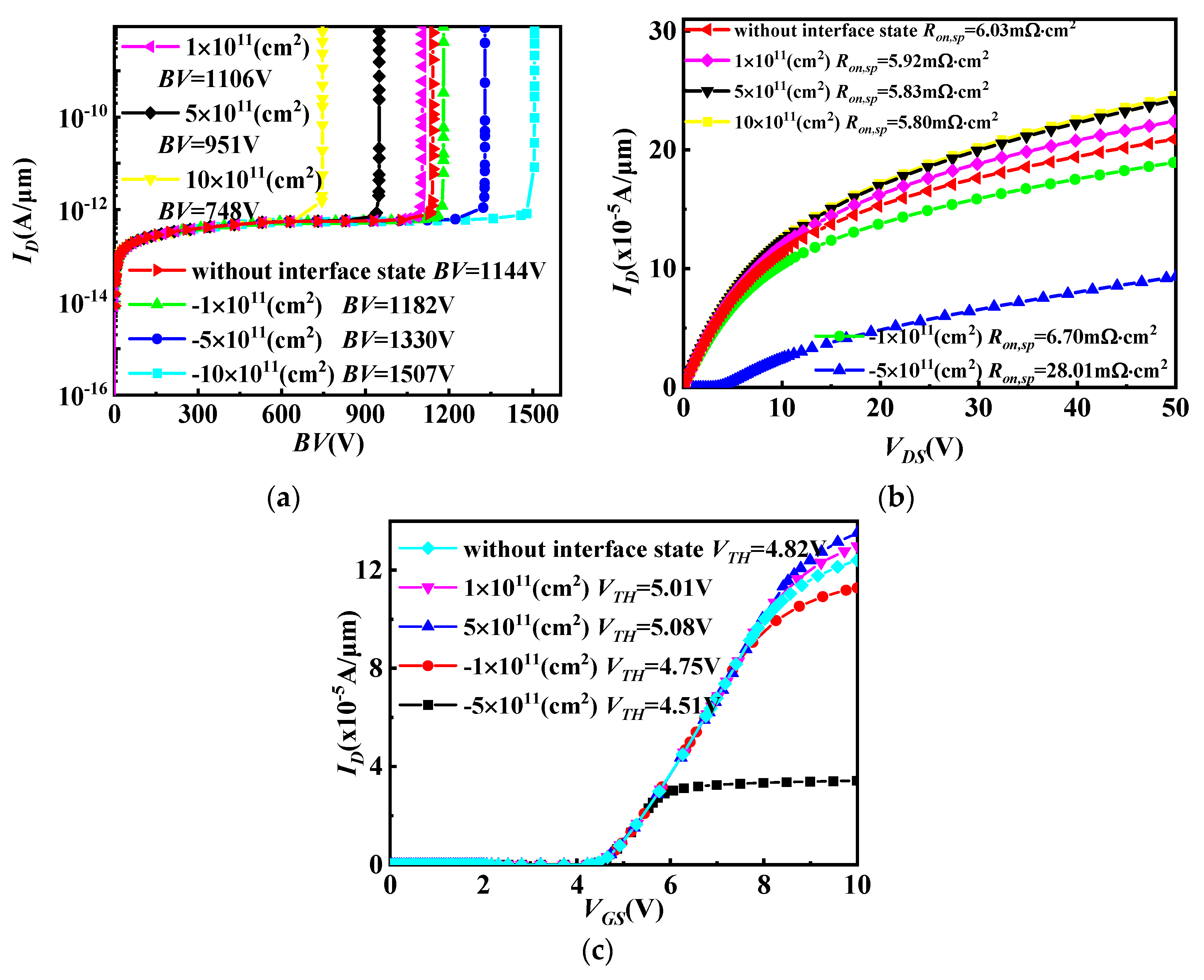
The optimized blocking characteristics and output characteristics for the SiC/Si VDMOS are provided in Figure 3a,b. As can be seen, BV was 1144 V, and Ron,sp was 6.03 mΩ·cm2 for the SiC/Si VDMOS without an interface state charge. The BV of the SiC/Si VDMOS increased from 1182 V to 1507 V with increasing interface state charges (acceptorlike) concentrations. This is because the vertical electric field of SiC/Si VDMOS increased by SiC/Si heterojunction, which the p-type trap layer introduced by the interface charge (acceptor) at the SiC/Si heterojunction, resulting in Ron,sp increasing to 28 mΩ·cm2. However, the internal electron barrier was induced in the inversion layer at the SiC/Si interface, and the number of electrons in the channel increased, resulting in an increase in the electron current. This resulted in Ron,sp dropping from 6.03 mΩ·cm2 to 5.80 mΩ·cm2, and BV decreased to 748 V at this time. The transfer characteristics for the SiC/Si VDMOS are shown in Figure 3c. It is reported that the charge at the SiC/Si interface had an influence on the I–V characteristics of the SiC/Si VDMOS. That is, when the interface charge donor (electron) concentration increased, the threshold voltage (VTH) of SiC/Si VDMOS increased from 4.82 V to 5.08 V. When the interface charge was considered an acceptor (hole), the VTH of the SiC/Si VDMOS decreased from 4.75 V to 4.51 V as the interface charge concentration increased from 1 × 10⁵/cm2 to 5 × 10⁵/cm2.
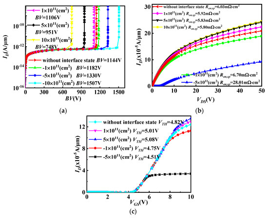
Figure 3.
(a) Blocking characteristics, (b) output characteristics, and (c) transfer characteristics for SiC/Si VDMOS with the different concentrations of interface state charge.
3.2. The Influence of Interface State on Band Energy Distributions
Figure 4 shows the energy bands of SiC/Si VDMOS, Si VDMOS, and SiC VDMOS during thermal equilibrium. It can be seen that for Si VDMOS, the bandgap was 1.12 eV, and the curve X = 2.5 μm was the focus of the Si VDMOS breakdown voltage (shown in Figure 1), which means that the breakdown point was located at the junction of the P-based and N-type drift regions, the site of the maximum radius of curvature of conventional Si VDMOS. Since the band gap of SiC VDMOS was 3.26 eV, curve X = 4.9 μm was the focal point of the SiC VDMOS breakdown voltage, and the BV of the device reached 1747 V. The curve X = 4.9 μm was the focus of the breakdown voltage for SiC/Si VDMOS with SiC/Si heterojunction (shown in Figure 1). Due to the high critical breakdown field strength of SiC materials, BV increased from 259 V to 1144 V compared with Si VDMOS.
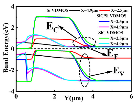
Figure 4.
The energy band diagram at thermal equilibrium for SiC/Si VDMOS, Si VDMOS, and SiC VDMOS.
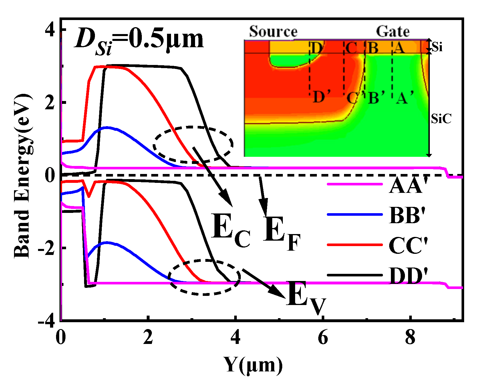
Figure 5 shows the band diagram of N−–Si/N–SiC in the middle of mesa (AA’), the P–Si/N–SiC heterojunction (BB’), the P–Si/P–SiC heterojunction (CC’), and the N+–Si/P–SiC heterojunction (DD’). To analyze the band state of the SiC/Si VDMOS heterojunction, four tangents in the y direction (AA’, BB’, CC’, and DD’) were chosen. We can see that the SiC/Si VDMOS heterojunction is affected not only by the two materials Si and SiC with different bandgaps but also by the doping concentration and different doping types at different regions of the device, which change the heterojunction bandgap of SiC/Si VDMOS.

Figure 5.
Band diagram of N−-Si/N−-SiC in the middle of mesa (AA’), the P-Si/N−-SiC heterojunction (BB’), the P-Si/P-SiC heterojunction (CC’), and the N+-Si/P-SiC heterojunction (DD’).
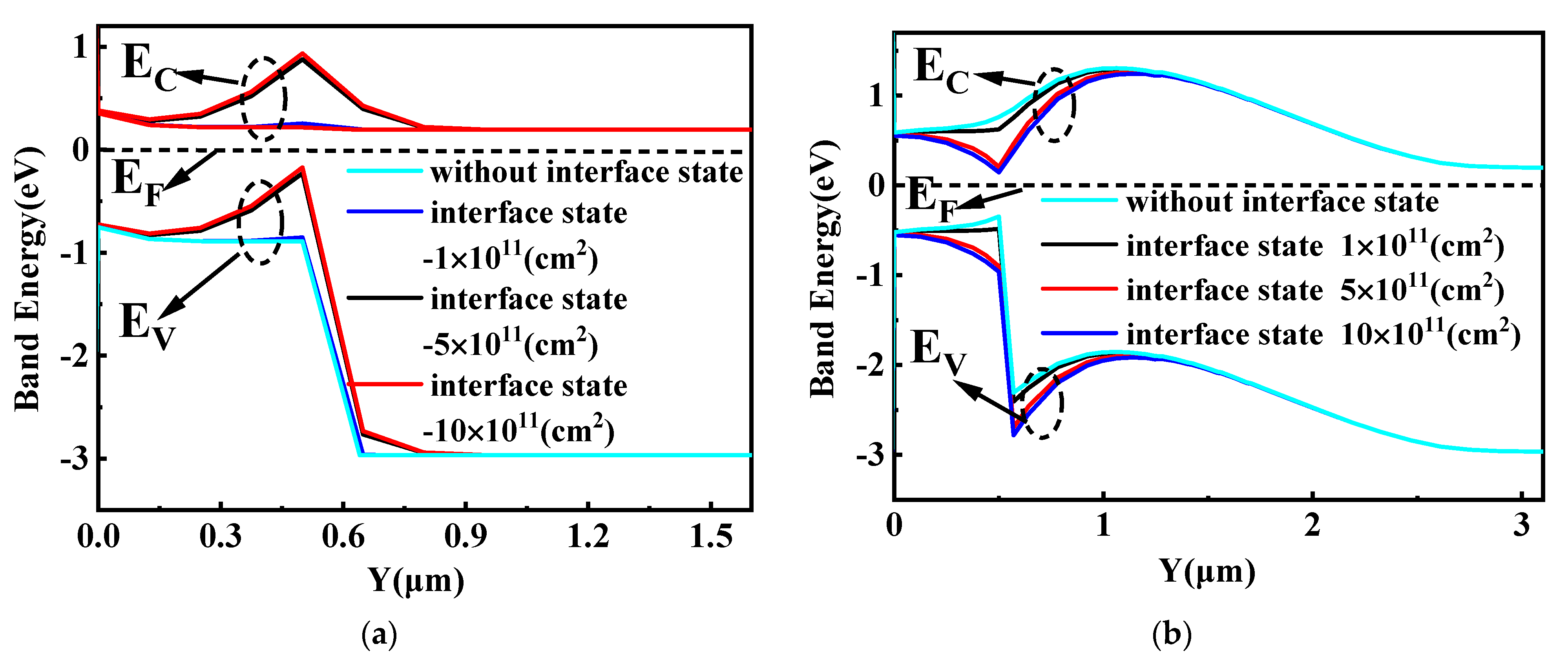
The energy band diagram of SiC/Si VDMOS with different interface state charges (acceptorlike) is shown in Figure 6a. In this figure, as the interface concentration increases, the energy at the SiC/Si heterojunction rises slightly due to the p-type trap layer introduced by the interface charge (acceptor) at the SiC/Si heterojunction interface. This results in an increase in the barrier height difference at the heterojunction, resulting in an increase in the BV of SiC/Si VDMOS (shown in Figure 3a). Further, since the height of the barrier becomes high, electrons do not easily flow, and thus, Ron,sp increases (shown in Figure 3b). Figure 6b shows the influence of different interface state charges (donors) on the energy band diagram of SiC/Si VDMOS. Electrons were induced in the inversion layer at the SiC/Si heterojunction interface. As the interface concentration increased, the number of electrons in the channel increased, resulting in an increase in the electron current. The decrease in the barrier height resulted in a decrease in the BV of SiC/Si VDMOS, which facilitated electron flow and caused a decrease in Ron,sp (shown in Figure 3a,b).

Figure 6.
(a) The influence of different interface state charges (acceptorlike) on the energy band diagram of SiC/Si VDMOS, and (b) the influence of different interface state charges (donor) on the energy band diagram of SiC/Si VDMOS: LD = 5 μm, DSi = 0.5 μm.
3.3. The Influence of Interface State on Temperature Effects
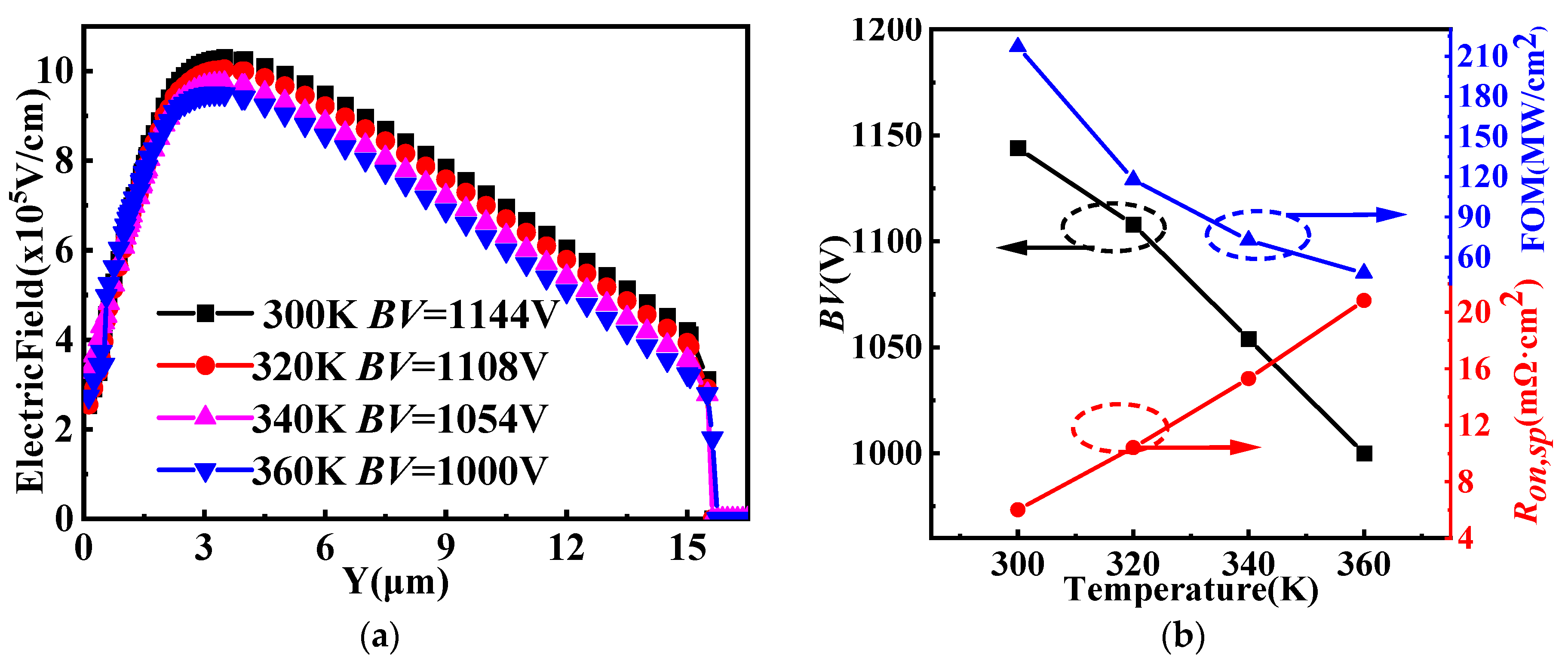
Figure 7a shows the vertical electric field distributions for SiC/Si VDMOS at the temperature range of 300 K to 360 K. It can be seen that the highest electric field of the SiC/Si VDMOS reached 9.8 MV/cm, and BV was 1144 V at 300 K [25,26,27,28,29]. When the temperature was increased to 360 K, the maximum electric field of the SiC/Si VDMOS dropped to 8.8 MV/cm, and BV dropped to 1000 V. The dependences of BV, Ron,sp, and figure-of-merit (FOM = BV2/Ron,sp) changes from 300 K to 360 K for the SiC/Si VDMOS are shown in Figure 7b. It was found that the BV of SiC/Si VDMOS decreased from 1144 V to 1000 V as the temperature increased. In addition, the Ron,sp of SiC/Si VDMOS increased, yielding a FOM (217 MW/cm2) of SiC/Si VDMOS that dropped to 48 MW/cm2.
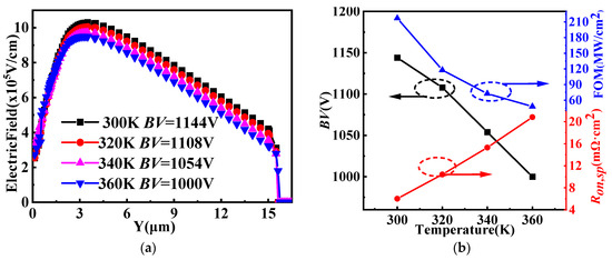
Figure 7.
(a) Vertical electric field distributions for SiC/Si VDMOS at a temperature range of 300 to 360 K, and (b) dependences of BV, Ron,sp, and figure-of-merit (FOM = BV2/Ron,sp) changes from 300 to 360 K for SiC/Si VDMOS.
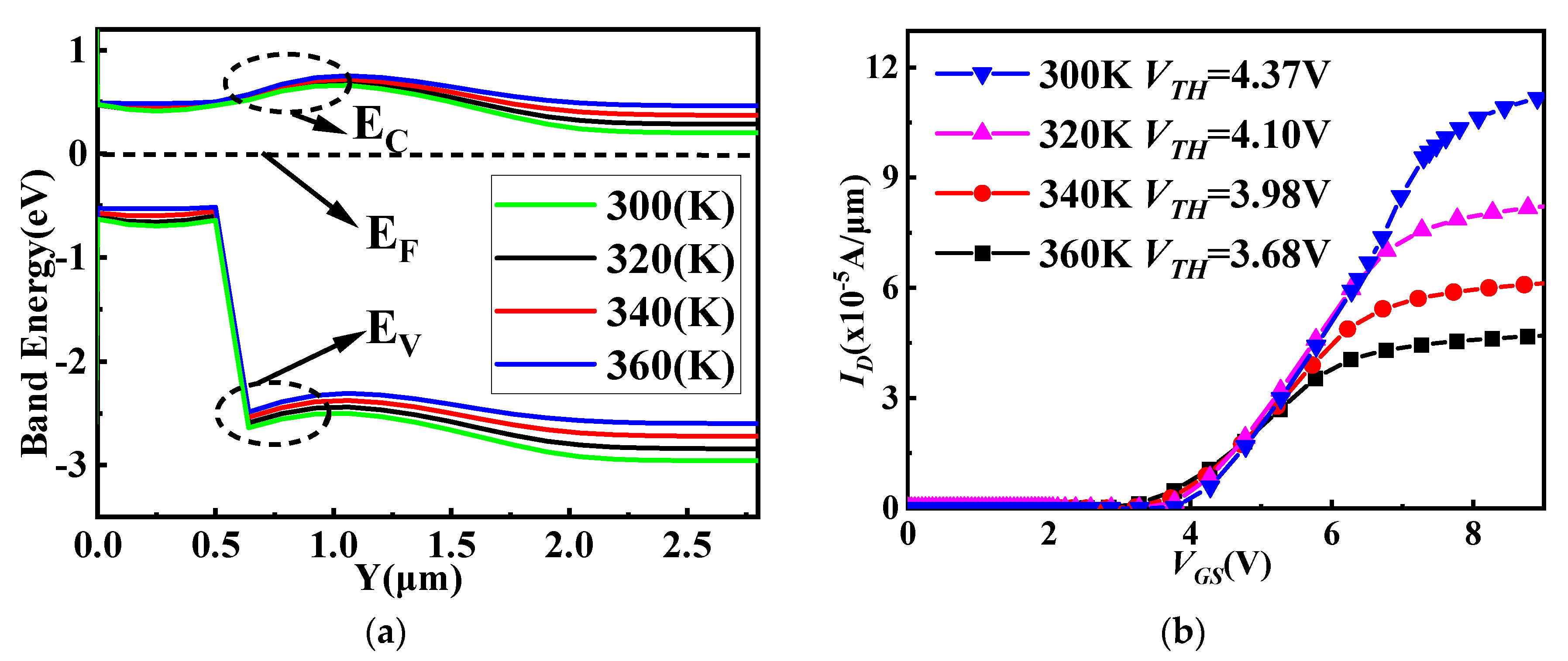
Figure 8a shows the band diagram of the P-Si/N−SiC heterojunction at a temperature range of 300 K to 360 K. The barrier height difference decreased when the temperature rose and BV decreased. At the same time, the resistivity and impurity ionization rate of the drift region increased as the temperature increased [37]. Transfer characteristics changes from 300 K to 360 K for the SiC/Si VDMOS are shown in Figure 8b. At 300 K, VTH was 4.37 V for SiC/Si VDMOS. As the temperature increased, the barrier height difference decreased, resulting in a decrease in the VTH of SiC/Si VDMOS. When the temperature reached 360 K, the VTH of the SiC/Si VDMOS was reduced to 3.68 V.

Figure 8.
(a) Band diagram of the P-Si/N−-SiC heterojunction at a temperature range of 300 to 360 K, and (b) transfer characteristic changes from 300 K to 360 K for SiC/Si VDMOS.
3.4. The Influence of Interface State on Interface Capacitances and Switching Performances
Figure 9 shows the reverse transfer capacitances (Crss) of SiC/Si VDMOS, Si VDMOS, and SiC VDMOS. Crss is especially important when VDMOS devices are used for power supplies due to the switching loss of the device being seriously affected. The expression for Crss is:
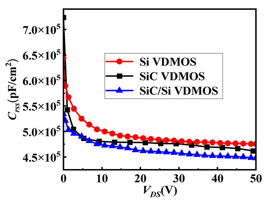
Figure 9.
Reverse transfer capacitances (Crss) of SiC/Si VDMOS, Si VDMOS, and SiC VDMOS.
As shown in Figure 9, the Crss of SiC/Si VDMOS was smaller than that of conventional Si VDMOS and SiC VDMOS. A new capacitor was introduced at the interface where the SiC/Si heterojunction was introduced, thereby reducing the depletion capacitance of the SiC/Si VDMOS.
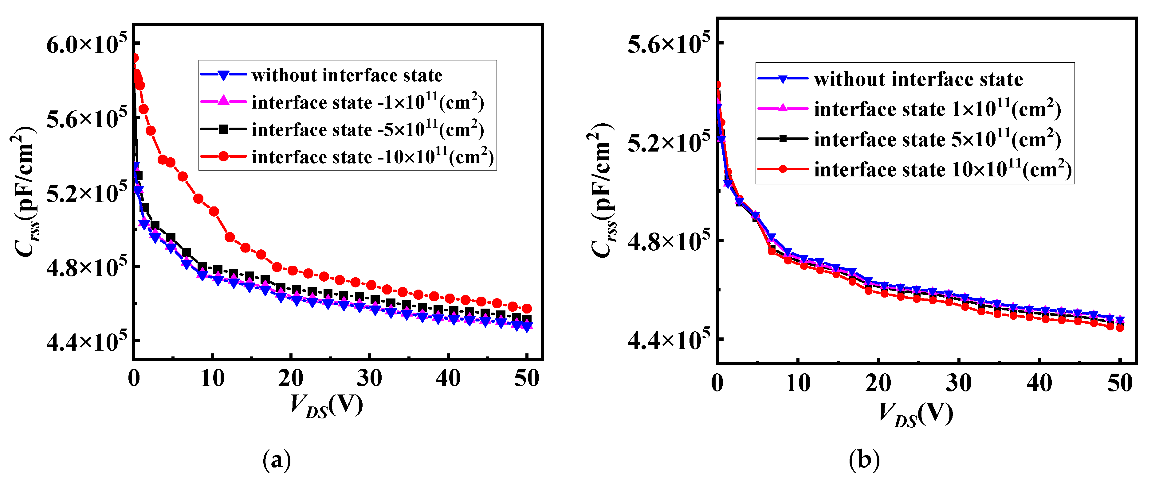
Figure 10a shows the influence of different interface state charges (acceptorlike) on the reverse transfer capacitances (Crss) for SiC/Si VDMOS. When the acceptor (hole) interface charge was considered, an opposite type of negative charge was induced at the channel of e SiC/Si VDMOS. This increased the depletion charge of the device, causing the Crss of SiC/Si VDMOSFET to increase as the interface concentration increased. The Crss of SiC/Si VDMOS with different interface state charges (donor) is shown in Figure 10b. A positive charge induced at the channel of the SiC/Si VDMOS reduced the depletion charge of SiC/Si VDMOS due to the interface charge donor (electron) being introduced at the SiC/Si interface. Therefore, as the concentration increased, the Crss of SiC/Si VDMOS decreased.

Figure 10.
(a) The influence of different interface state charges (acceptorlike) on the reverse transfer capacitances (Crss) for SiC/Si VDMOS, and (b) the influence of different interface state charges (donor) on the reverse transfer capacitances (Crss) for SiC/Si VDMOS.
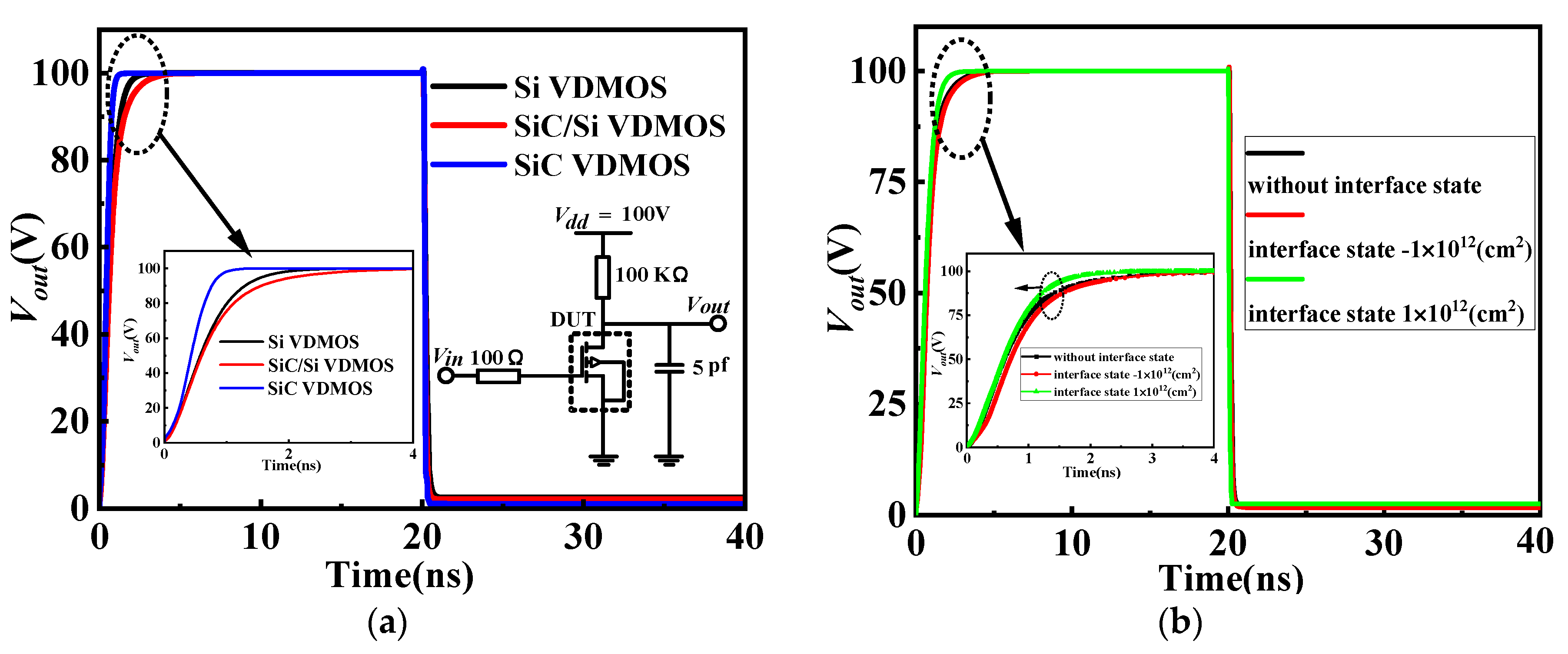
Figure 11a shows the dynamic performance of the three devices under resistive load. It can be seen that the turn-OFF speed of SiC VDMOS was lower than that of SiC/Si VDMOS and Si VDMOS. The dynamic characteristics of the proposed device were more suitable for low and medium frequencies in the power field, while the turn-ON speed for the two devices was almost the same. Figure 11b shows the influence of different interface state charges on the switching characteristics for SiC/Si VDMOS. A positive charge was induced at the channel of the SiC/Si VDMOS due to the interface charge donor (electron) being introduced. This reduced the depletion charge of the device, resulting in a faster turn-OFF speed of SiC/Si VDMOS. When the acceptor (hole) interface charge was considered, the depletion charge of the device increased. This resulted in a slower turn-OFF of SiC/Si VDMOS, while the turn-ON speed for the three cases was almost the same. The dynamic characteristics of the SiC/Si VDMOS were more suitable for low and medium frequencies in the power field.
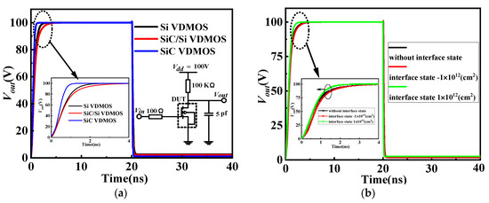
Figure 11.
(a) Switching characteristics under resistive load for the SiC/Si VDMOS, Si VDMOS, and SiC VDMOS, and (b) the influence of different interface state charges on the switching characteristics for SiC/Si VDMOS.
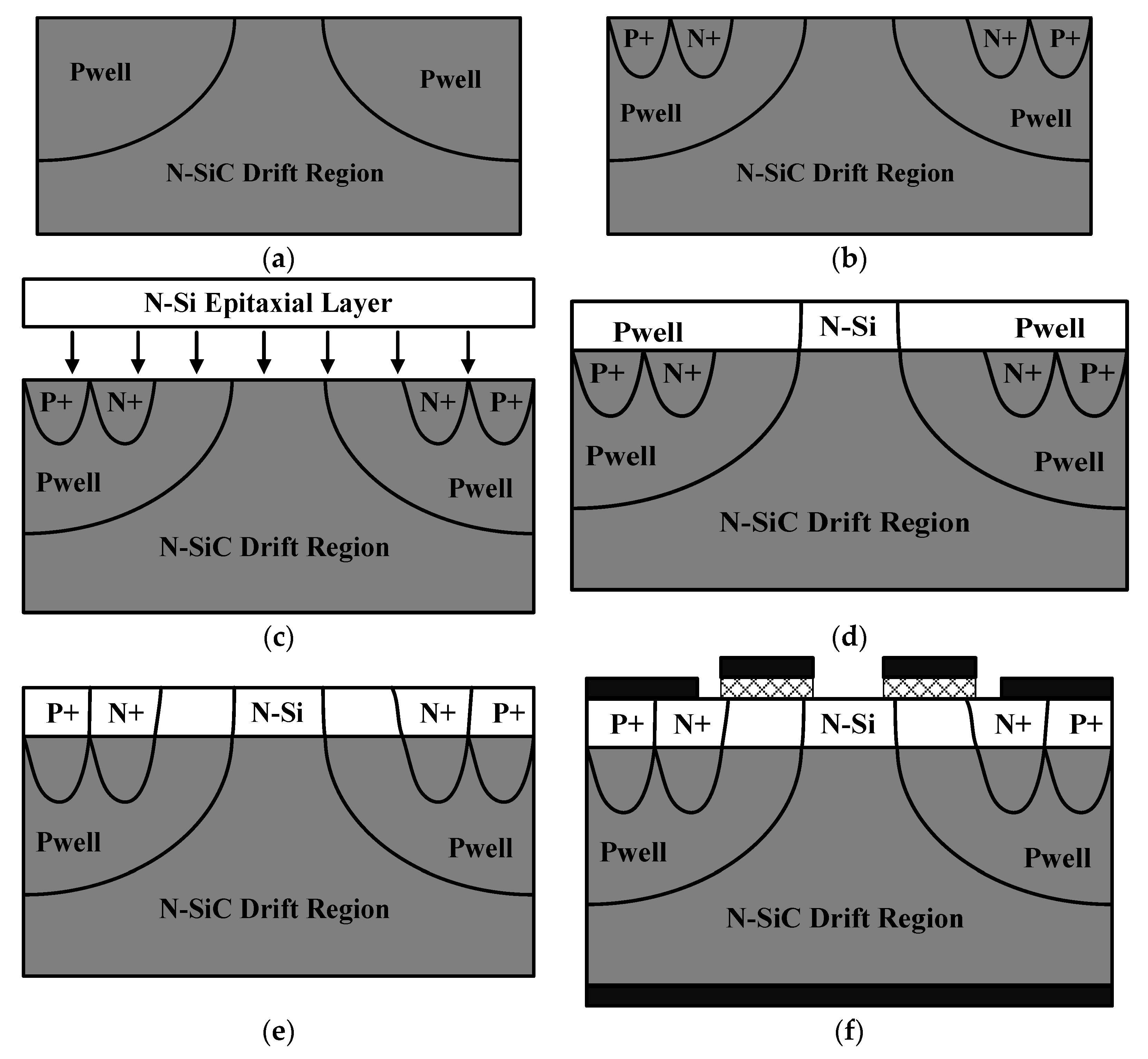
The key processes for the feasibility of manufacturing SiC/Si VDMOS are shown in Figure 12, and some key processes are similar to Si VDMOS. The formation of the SiC/Si drift region can be achieved by the method in Ref. [22]. The simplified wafer bonding process is as follows: (a) ion implantation forms a P-well in the N–SiC drift region; (b) ion implantation to form source region; (c) epitaxial growth of N–Si Layer; (d) wafer bonding is carried out and ion implantation is made to form the portion of the P-well in the N–Si layer; (e) ion implantation to form the portion of the source in the N–Si layer; and (f) the gate oxide layer grows, the field oxide layer grows, and then the source electrode and the drain electrode are contacted.

Figure 12.
(a–f) is a simplified key process for manufacturing SiC/Si VDMOS.
4. Conclusions
SiC/Si VDMOS and GaN/Si VDMOS were proposed in our previous paper; however, only the electrical and structural parameters of the device were studied. In the present study, SiC/Si VDMOS was optimized based on breakdown point transfer technology, and the influence of the band interface state on the device was analyzed. The BV of the SiC/Si heterojunction VDMOS was considerably increased from 259 V to 1144 V, and Ron,sp decreased from 18.2 mΩ·cm2 to 6.03 mΩ·cm2. Simulation results showed that the type and concentration of interface charges have a great influence on the electric field, blocking characteristics, output characteristics, transfer characteristics, and energy band distributions of SiC/Si VDMOS but have little effect on the capacitance characteristics and switching performances. As the positive concentration acceptor (hole) increased, the energy at the SiC/Si heterojunction rose slightly, resulting in an increase in BV. As the negative concentration donor (electron) increased, a decrease in the barrier height resulted in a decrease in the Ron,sp of BV. The electrical characteristics of SiC/Si VDMOS were changed when the temperature was raised, resulting in a negative temperature coefficient for BV and VTH but a positive temperature coefficient for Ron,sp.
Author Contributions
Project administration, B.D. and Y.Y.; writing—original draft preparation X.Y. All authors have read and agreed to the published version of the manuscript.
Funding
This research was funded by Science Foundation for Distinguished Young Scholars of Shaanxi Province, grant number 2018JC-017 and 111 Project, grant number B12026.
Institutional Review Board Statement
Not applicable.
Informed Consent Statement
Not applicable.
Data Availability Statement
Not applicable.
Conflicts of Interest
The authors declare no conflict of interest.
References
- Baliga, B.J. Fundamentals of Power Semiconductor Devices; Springer-Science: New York, NY, USA, 2008. [Google Scholar]
- Thapar, N.; Baliga, B. Influence of the Trench Corner Design on Edge Termination of UMOS Power Devices. Solid-State Electron. 1997, 41, 1929–1936. [Google Scholar] [CrossRef]
- Chen, X.-B.; Sin, J. Optimization of the specific on-resistance of the COOLMOS. IEEE Trans. Electron Devices 2001, 48, 344–348. [Google Scholar] [CrossRef]
- Lidow, A.; Herman, T.; Collins, H.W. Power MOSFET technology. In Proceedings of the International Electron Devices Meeting, Washington, DC, USA, 3–5 December 1979; Volume 25, pp. 79–85. [Google Scholar] [CrossRef]
- Baliga, B.J. The future of power semiconductor device technology. Proc. IEEE 2001, 89, 822–832. [Google Scholar] [CrossRef]
- Huang, H.M.; Chen, X.-B. Optimization of Specific On-Resistance of Balanced Symmetric Super junction MOSFETs Based on a Better Approximation of Ionization Integral. IEEE Trans. Electron Devices 2012, 59, 2742–2747. [Google Scholar] [CrossRef]
- Udrea, F.; Deboy, G.; Fujihira, T. Superjunction Power Devices, History, Development, and Future Prospects. IEEE Trans. Electron Devices 2017, 64, 713–727. [Google Scholar] [CrossRef]
- Luo, X.; Jiang, Y.H.; Zhou, K.; Wang, P.; Wang, X.W.; Wang, Q.; Yao, G.L.; Zhang, B.; Li, Z.J. Ultralow Specific On-Resistance Superjunction Vertical DMOS With High-K Dielectric Pillar. IEEE Electron Device Lett. 2012, 33, 1042–1044. [Google Scholar] [CrossRef]
- Luo, X.; Tan, Q.; Wei, J.; Zhou, K.; Deng, G.; Li, Z.; Zhang, B. Ultralow ON-Resistance High-Voltage p-Channel LDMOS With an Accumulation-Effect Extended Gate. IEEE Trans. Electron Devices 2016, 63, 2614–2619. [Google Scholar] [CrossRef]
- Ohta, K.; Morimoto, M.; Saitoh, M.; Fukuda, T.; Morino, A.; Shimizu, K.; Hayashi, Y.; Tarui, Y. A high-speed logic LSI using diffusion self-aligned enhancement depletion MOS IC. IEEE J. Solid-State Circuits 1975, 10, 314–321. [Google Scholar] [CrossRef]
- Chen, X.; Huang, M. A Vertical Power MOSFET With an Interdigitated Drift Region Using High-k Insulator. IEEE Trans. Electron Devices 2012, 59, 2430–2437. [Google Scholar] [CrossRef]
- Cao, Z.; Duan, B.X.; Cai, H.; Yuan, S.; Yang, Y.T. Theoretical Analyses of Complete 3-D Reduced Surface Field LDMOS With Folded-Substrate Breaking Limit of Superjunction LDMOS. IEEE Trans. Electron Devices 2016, 63, 4865–4872. [Google Scholar] [CrossRef]
- Duan, B.; Cao, Z.; Yuan, X.; Yuan, S.; Yang, Y. New Superjunction LDMOS Breaking Silicon Limit by Electric Field Modulation of Buffered Step Doping. IEEE Electron Device Lett. 2014, 36, 47–49. [Google Scholar] [CrossRef]
- Duan, B.; Cao, Z.; Yuan, S.; Yang, Y. Complete 3D-Reduced Surface Field Superjunction Lateral Double-Diffused MOSFET Breaking Silicon Limit. IEEE Electron Device Lett. 2015, 36, 1348–1350. [Google Scholar] [CrossRef]
- Duan, B.; Yang, Y. REBULF super junction MOSFET with N+ buried layer. Micro Nano Lett. 2011, 6, 881–883. [Google Scholar] [CrossRef]
- Duan, B.; Yang, X.; Lv, J.; Yang, Y. Novel SiC/Si Heterojunction Power MOSFET With Breakdown Point Transfer Terminal Technology by TCAD Simulation Study. IEEE Trans. Electron Devices 2018, 65, 3388–3393. [Google Scholar] [CrossRef]
- Duan, B.; Lv, J.; Zhao, Y.; Yang, Y. SiC/Si heterojunction VDMOS breaking silicon limit by breakdown point transfer technology. Micro Nano Lett. 2018, 13, 96–99. [Google Scholar] [CrossRef]
- Yang, X.; Duan, B.; Yang, Y. GaN/Si Heterojunction VDMOS with High Breakdown Voltage and Low Specific On-Resistance. Micromachines 2023, 14, 1166. [Google Scholar] [CrossRef]
- Zhao, D.; Wang, Y.; Chen, Y.; Shao, J.; Fu, Z.; Duan, B.; Liu, F.; Li, X.; Li, T.; Yang, X.; et al. Novel Step Floating Islands VDMOS with Low Specific on-Resistance by TCAD Simulation. Micromachines 2022, 13, 573. [Google Scholar] [CrossRef]
- Saddow, S.E.; Frewin, C.L.; Nezafati, M.; Oliveros, A.; Afroz, S.; Register, J.; Reyes, M.; Thomas, S. 3C-SiC on Si: A bio- and hemo-compatible material for advanced nano-bio devices. In Proceedings of the 2014 IEEE 9th Nanotechnology Materials and Devices Conference (NMDC), Aci Castello, Italy, 12–15 October 2014; pp. 49–53. [Google Scholar]
- Kukushkin, S.A.; Osipov, A.V. Theory and practice of SiC growth on Si and its applications to wide-gap semiconductor films. J. Phys. D. Appl. Phys. 2014, 47, 313001. [Google Scholar] [CrossRef]
- Jennings, M.R.; Pérez-Tomás, A.; Guy, O.J.; Hammond, R.; Burrows, S.E.; Gammon, P.M.; Lodzinski, M.; Covington, J.A.; Mawby, P.A. Si/SiC Heterojunctions Fabricated by Direct Wafer Bonding. Electrochem. Solid-State Lett. 2008, 11, H306–H308. [Google Scholar] [CrossRef]
- Gammon, P.M.; Chan, C.W.; Li, F.; Gity, F.; Trajkovic, T.; Pathirana, V.; Flandre, D.; Kilchytska, V. Development, characterisation and simulation of wafer bonded Si-on-SiC substrates. Mater. Sci. Semicond. Process. 2018, 78, 69–74. [Google Scholar] [CrossRef]
- Sasada, Y.; Kurumi, T.; Shimizu, H.; Kinoshita, H.; Yoshimoto, M. Junction Formation via Direct Bonding of Si and 6H-SiC. Mater. Sci. Forum 2014, 778–780, 714–717. [Google Scholar] [CrossRef]
- Hayashi, T.; Tanaka, H.; Shimoida, Y.; Tanimoto, S.; Hoshi, M. New High-Voltage Unipolar Mode p+ Si/n− 4H-SiC Heterojunction Diode. Mater. Sci. Form 2005, 483–485, 953–956. [Google Scholar] [CrossRef]
- Chen, L.; Guy, O.; Jennings, M.; Igic, P.; Wilks, S.; Mawby, P. Study of a novel Si/SiC hetero-junction MOSFET. Solid-State Electron. 2007, 51, 662–666. [Google Scholar] [CrossRef]
- Liang, J.; Nishida, S.; Hayashi, T.; Arai, M.; Shigekawa, N. Effects of interface state charges on the electrical properties of Si/SiC heterojunctions. Appl. Phys. Lett. 2014, 105, 151607. [Google Scholar] [CrossRef]
- Williams, R.K.; Darwish, M.N.; Blanchard, R.A.; Siemieniec, R.; Rutter, P.; Kawaguchi, Y. The Trench Power MOSFET: Part I—History, Technology, and Prospects. IEEE Trans. Electron Devices 2017, 64, 674–691. [Google Scholar] [CrossRef]
- Williams, R.K.; Darwish, M.N.; Blanchard, R.A.; Siemieniec, R.; Rutter, P.; Kawaguchi, Y. The Trench Power MOSFET—Part II: Application Specific VDMOS, LDMOS, Packaging, and Reliability. IEEE Trans. Electron Devices 2017, 64, 692–712. [Google Scholar] [CrossRef]
- Sung, W.; Baliga, B.J. Monolithically Integrated 4H-SiC MOSFET and JBS Diode (JBSFET) Using a Single Ohmic/Schottky Process Scheme. IEEE Electron Device Lett. 2016, 37, 1605–1608. [Google Scholar] [CrossRef]
- Sung, W.; Baliga, B.J. A Near Ideal Edge Termination Technique for 4500V 4H-SiC Devices: The Hybrid Junction Termination Extension. IEEE Electron Device Lett. 2016, 37, 1609–1612. [Google Scholar] [CrossRef]
- Tega, N.; Hisamoto, D.; Shima, A.; Shimamoto, Y. Channel Properties of SiC Trench-Etched Double-Implanted MOS (TED MOS). IEEE Trans. Electron Devices 2016, 63, 3439–3444. [Google Scholar] [CrossRef]
- Ni, W.; Emori, K.; Marui, T.; Saito, Y.; Yamagami, S.; Hayashi, T.; Hoshi, M. SiC Trench MOSFET with an Integrated Low Von Unipolar Heterojunction Diode. Mater. Sci. Forum 2014, 778–780, 923–926. [Google Scholar] [CrossRef]
- Nazarov, A.N.; Vovk, Y.N.; Lysenko, V.S.; Turchanikov, V.I.; Scryshevskii, V.A.; Ashok, S. Carrier transport in amorphous SiC/crystalline silicon heterojunctions. J. Appl. Phys. 2001, 89, 4422–4428. [Google Scholar] [CrossRef]
- Gammon, P.M.; Pérez-Tomás, A.; Jennings, M.R.; Sanchez, A.M.; Fisher, C.A.; Thomas, S.M.; Donnellan, B.T.; Mawby, P.A. Bipolar Conduction across a Wafer Bonded p-n Si/SiC Heterojunction. Mater. Sci. Forum 2013, 740–742, 1006–1009. [Google Scholar] [CrossRef]
- Su, J.; Niu, Q.; Zhang, D.; Zhang, Y.; Fu, Z. Carrier transport mechanisms of p-SiC/n-Si hetero-junctions. Solid State Sci. 2011, 13, 434–437. [Google Scholar] [CrossRef]
- Nishida, S.; Liang, J.; Hayashi, T.; Arai, M.; Shigekawa, A. Correlation between the electrical properties of p-Si/n-4H-SiC junctions and concentrations of acceptors in Si. Jpn. J. Appl. Phys. 2015, 54, 030210. [Google Scholar] [CrossRef]
- Raghunathan, R.; Alok, D.; Baliga, B. High voltage 4H-SiC Schottky barrier diodes. IEEE Electron Device Lett. 1995, 16, 226–227. [Google Scholar] [CrossRef]
- Raghunathan, R.; Baliga, B.J. Role of defects in producing negative temperature dependence of breakdown voltage in SiC. Appl. Phys. Lett. 1998, 72, 3196–3198. [Google Scholar] [CrossRef]
- Kimoto, T.; Urushidani, T.; Kobayashi, S.; Matsunami, H. High-voltage (>1 kV) SiC Schottky barrier diodes with low on-resistances. IEEE Electron Device Lett. 1993, 14, 548–550. [Google Scholar] [CrossRef]
- Licciardo, G.D.; Di Benedetto, L.; Bellone, S. Modeling of the SiO2/SiC Interface-Trapped Charge as a Function of the Surface Potential in 4H-SiC Vertical-DMOSFET. IEEE Trans. Electron Devices 2016, 63, 1783–1787. [Google Scholar] [CrossRef]
- Wang, Y.; Ma, Y.-C.; Hao, Y.; Hu, Y.; Wang, G.; Cao, F. Simulation Study of 4H-SiC UMOSFET Structure With p+-polySi/SiC Shielded Region. IEEE Trans. Electron Devices 2017, 64, 3719–3724. [Google Scholar] [CrossRef]
- Wang, Y.; Wang, H.-Y.; Cao, F.; Wang, H.-Y. High Performance of Polysilicon/4H-SiC Dual-Heterojunction Trench Diode. IEEE Trans. Electron Devices 2017, 64, 1653–1659. [Google Scholar] [CrossRef]
- Chan, C.; Mawby, P.A.; Gammon, P.M. Analysis of Linear-Doped Si/SiC Power LDMOSFETs Based on Device Simulation. IEEE Trans. Electron Devices 2016, 63, 2442–2448. [Google Scholar] [CrossRef]
- Chan, C.W.; Li, F.; Sanchez, A.; Mawby, P.A.; Gammon, P.M. Comparative study of RESURF Si/SiC LDMOSFETs for high-temperature applications using TCAD modeling. IEEE Trans. Electron Devices 2017, 64, 3713–3718. [Google Scholar] [CrossRef]
- Araki, R.; Shimizu, H.; Kurumi, T.; Kinoshita, H.; Yoshimoto, M. Drain current -gate voltage characteristics of Si MOSFETs fabricated on Si-on-SiC wafers. In Proceedings of the 2011 International Meeting for Future of Electron Devices, Osaka, Japan, 19–20 May 2011; pp. 68–69. [Google Scholar]
- Tanaka, H.; Hayashi, T.; Shimoida, Y.; Yamagami, S.; Tanimoto, S.; Hoshi, M. Ultra-low von and high voltage 4H-SiC heterojunction diode. In Proceedings of the 17th International Symposium on Power Semiconductor Devices and ICs, Santa Barbara, CA, USA, 23–26 May 2005; pp. 287–290. [Google Scholar] [CrossRef]


Disclaimer/Publisher’s Note: The statements, opinions and data contained in all publications are solely those of the individual author(s) and contributor(s) and not of MDPI and/or the editor(s). MDPI and/or the editor(s) disclaim responsibility for any injury to people or property resulting from any ideas, methods, instructions or products referred to in the content. |
© 2023 by the authors. Licensee MDPI, Basel, Switzerland. This article is an open access article distributed under the terms and conditions of the Creative Commons Attribution (CC BY) license (https://creativecommons.org/licenses/by/4.0/).