4.1. Temperature Cycling Test Results
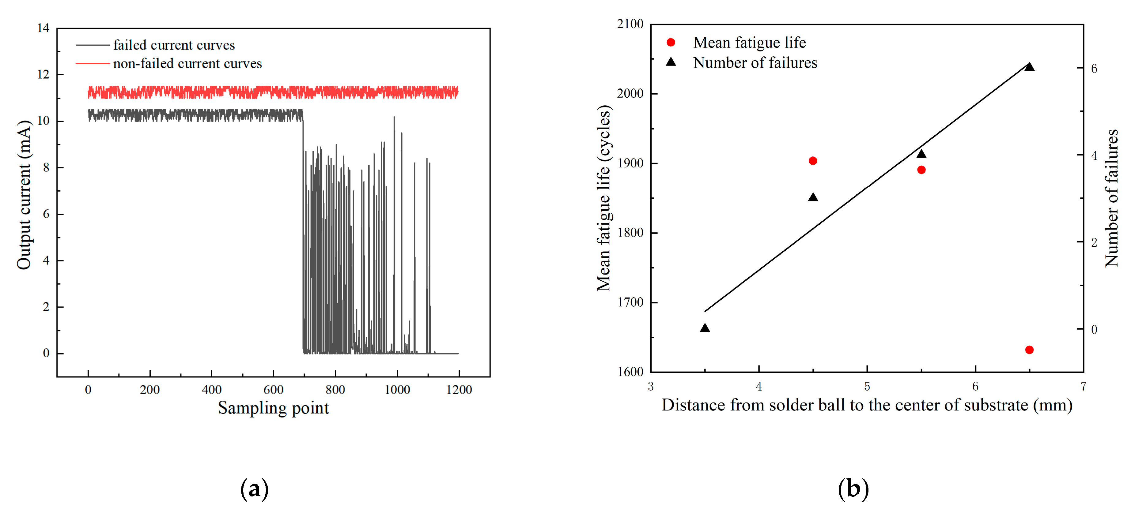
Figure 3a shows the typical output current curves of failed and non-failed samples. A stable current signal could always be received from the non-failed samples. For signals from failed samples, the failure can be identified at the first drop from over 10 mA to 0 mA, which was caused by the open circuit. The following spikes in the curve can be attributed to occasional contacts at the failed sites by the vibration of the chamber during the test. Thermal fatigue results are summarized in
Figure 3b. A total of 13 rings’ solder joint failures were monitored in the temperature cycling test.
As can be seen from
Figure 3b, the mean fatigue life of the solder balls decreased with the increase in distance between the solder balls and the geometric center of the BT substrate. Correspondingly, the number of failed solder balls increases as this distance increases. The innermost solder balls all survived after 2325 temperature cycles. The reason for this difference is that the amount of inelastic deformation by the mismatch of CTE is proportional to the distance from the solder ball to the geometric center of the substrate.
Since only 10.8% of the samples failed the tests, the right censored Weibull distribution [
18] was used to fit the failure data. According to the calculation, the shape parameter, β, and characteristic life, η, of the Weibull distribution in the cycles-to-failure (CTF) are 3.67 and 4184 cycles for the temperature cycling test, respectively.
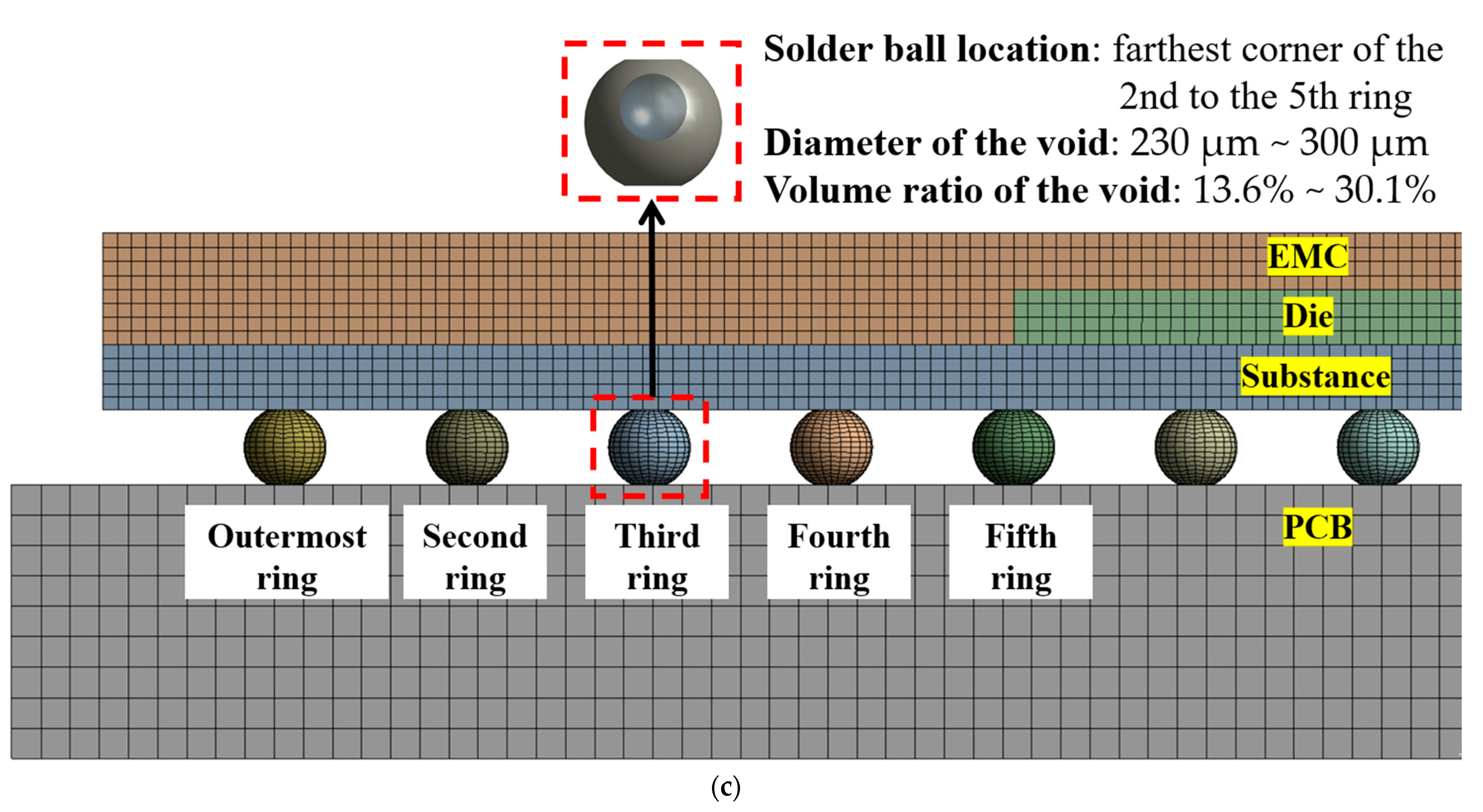
An X-ray was carried out on all 30 BGA board-level samples after the temperature cycling test. The three solder balls marked in
Figure 4b had typical open circuit failures, which were located in the outermost two rings of all solder balls. No failures or defects could be identified in solder balls closer to the geometric center. The void area ratio was calculated based on the X-ray projection images of BGA samples before and after the temperature cycle tests, as shown in
Figure 4c. It was found that the mean void area ratio decreases with the drop in distance between the solder balls and the geometric center. After the thermal cycle test of 5037 h, the area of void in the failed solder joint of the outermost ring was still smaller than that allowed by IPC-A 610E. Although voids were also found in the solder balls of the fourth and fifth rings, there were no failed solder joints due to smaller voids.
The results of the dye and pry test are shown in
Figure 5. The red area in
Figure 5a was the disconnected area caused by thermal fatigue, which has been stained by red ink. The white area was still connected after the thermal fatigue test, so it was not stained by red ink. Compared with
Figure 5a,b, it can be seen that the disconnection area is mainly composed of A, B, and C, and their enlarged images are shown in
Figure 5c. Similar lamellar morphology can be seen in
Figure 5c(A,C) with obvious cracks between them. Area B is porous and granular. EDS results show that area B contains 70 wt.% carbon, which is caused by red ink. Element distribution scanning was carried out for the whole section of the solder joint, and component analysis was carried out for the local parts. The results show that there was no IMC on the fracture surface, which indicates that the fracture occurred near the solder/IMC interface but that no crack passed through the IMC layer.
4.2. Finite Element Analysis Results
To evaluate the effects of voids on the fatigue life of solder joints, a BGA model with no voids was first investigated (case 1).
Figure 6a is the equivalent von Mises stress distribution of the outermost solder ball after five cycles of temperature cycling loading. The maximum equivalent stress and strain were located at the solder/chip interface at the outermost corner. This solder ball was the one farthest from the geometric center of the substrate and is often referred to as the “dangerous solder ball”. It was found that the “dangerous solder ball” is a weak link, which generally leads to the first failure of the packaging module [
19].
Figure 7 shows the evolution of the equivalent von Mises stress and accumulated equivalent plastic strain of four outer rings’ solder balls under the temperature cycling load. The equivalent stress changes periodically with time. However, the amplitude of the equivalent stress dropped with a lower distance to the geometric center.
Figure 7b shows that the accumulated plastic strain generally increased as the test continued with the highest rate at the outermost ring. This will also lead to the final failure of solder balls.
A strain-based Engelmaier-modified Coffin-Manson fatigue life prediction model [
20] was used to calculate the fatigue life of solder balls in the BGA package. For lead-free solder balls of SAC305, the formula for calculating the fatigue life
Nf is as follows:
where Δγ is the equivalent inelastic shear strain range, Δγ = √3Δε; Δε is the equivalent inelastic total strain range; ε
f is the fatigue toughness coefficient, ε
f = 0.48; and
c is the fatigue toughness index, which is related to the temperature and frequency of the temperature cycle.
where,
Tsj is the average temperature of the temperature cycle (°C), and
tD is the half-cycle dwell time in minutes. As can be seen from
Figure 8, the equivalent plastic strain accumulated in a single cycle tends to be stable after the first cycle. Therefore, it is normally recommended to use the accumulated equivalent plastic strain in the fifth cycle to calculate the fatigue life of solder balls.
Based on the accumulated equivalent plastic strain in
Figure 7b and Equations (1) and (2), the fatigue life of the solder balls was calculated and listed in
Table 5. The fatigue life decreased with a higher distance to the geometric center. The fatigue life of the “dangerous solder ball” located at the outermost corner was 4014 cycles from FEA, which was 4.1% different from the characteristic life of a solder ball obtained by the BGA thermal cycling test. This shows that the results of the simulation and experiment were consistent.
To further investigate the influences of voids on the thermal fatigue reliability of BGA, voids with progressively increasing diameters were introduced within solder balls at typical locations (case 2–21 in
Table 4). The typical results of the comparison of the stress and strain distribution between case 2 with a void and case 1 without a void are shown in
Table 6. It can be seen that the effects of the void in the solder joint of the second ring on the equivalent stress and strain of the outermost rings in case 2 were extremely small when comparing the stress/strain distribution of the outermost solder balls in case 1 and case 2. When comparing the solder ball at the second ring in case 2 with the solder balls at the outermost and second rings in case 1, it showed that the macro void could not affect the locations of maxima but that the stress and strain concentrations at the solder/chip interface deteriorated severely with the introduction of voids. This leads to the increase of the maximum stress/strain in the solder ball with a void at the second ring in case 2, which will likely exceed the maxima of the outermost solder ball in case 1.
Figure 9 shows the accumulated equivalent plastic strain of solder joints on the outermost ring in case 1 and the second ring in cases 2–6. The accumulated equivalent plastic strain of solder balls on the second ring will gradually increase with a larger void volume and even exceed that of the outermost ones without voids. In this process, a critical void volume ratio can be determined, which makes the accumulated plastic strain of the solder ball on the second ring equivalent to the outermost ones, such as in case 1 and case 4 in
Figure 9. According to formulas 1 and 2, the fatigue life of the two was also equivalent.
Based on the simulations listed in
Table 4, the similar effects of the void volume on the accumulated plastic strain can also be identified in solder balls at other inner rings, as summarized in
Figure 10a. It can be found that for solder balls at different inner rings, the accumulated plastic strain generally increased linearly with the void volume from less than that at the outermost solder ball in case 1 to surpassing it. Therefore, there is always a critical void volume for solder balls at the inner rings, at which the accumulated plastic strain in solder balls at inner rings was equivalent to that in the outermost solder ball (the interception points in
Figure 10a).
Based on Equations (1) and (2), the thermal fatigue life of solder balls from simulations in
Table 4 is also evaluated and summarized in
Figure 10b. In contrast to accumulated plastic strain, the increase in void volume led to a significant drop in fatigue life. The slopes of the fitted curves gradually decreased with a lower distance to the geometric center. This means that the fatigue life of solder joints farther from the geometric center tends to be more sensitive to void sizes, which can also be attributed to the fact that the solder joint of the outer ring withstands greater inelastic strain from the mismatch of CTE.
Furthermore, from
Figure 11, the critical void volume ratio dropped linearly with a higher distance to the geometric center. It can be expressed as:
where
x is the distance from the solder ball to the center of the substrate, and
y is the critical void volume ratio. The solder ball closer to the interior can withstand larger voids. Among them, for the solder joints of the second and third rings, when the void volume ratio exceeded 10.5% and 19.6%, respectively, their increased rate of accumulated inelastic strain during thermal cycling would exceed the outermost ones without voids, so that failures occurred first. This is also the reason why partial failures were also monitored in the second and third rings’ solder joints in the thermal cycling tests. However, the critical void volume ratio in the fourth and fifth rings’ solder joints reached 30.1% and 42.3%, respectively. Such a large void can seldom be found in solder balls [
21,
22]. This is also the reason why no thermal fatigue failure can be found within the fourth ring in the temperature cycling test. The results of this study show that the solder balls on the inner ring have a stronger tolerance to voids. However, the requirements of the current standards on the voids of solder joints are half-baked and oversimplified. For example, IPC-A 610E requires that voids in X-ray images not exceed 30% of the area of a single solder ball. In addition, from the perspective of practical application, the fatigue life of the BGA module and the tolerance of deviation in the process parameter can be significantly improved by adding several rings of solder joints outside the solder joints of key functions.


