


Multi Frequency Controllable In-Band Suppressions in a Broad Bandwidth Microstrip Filter Design for 5G Wi-Fi and Satellite Communication Systems Utilizing a Quad-Mode Stub-Loaded Resonator


 , , ,
, , , 
Abstract
:1. Introduction
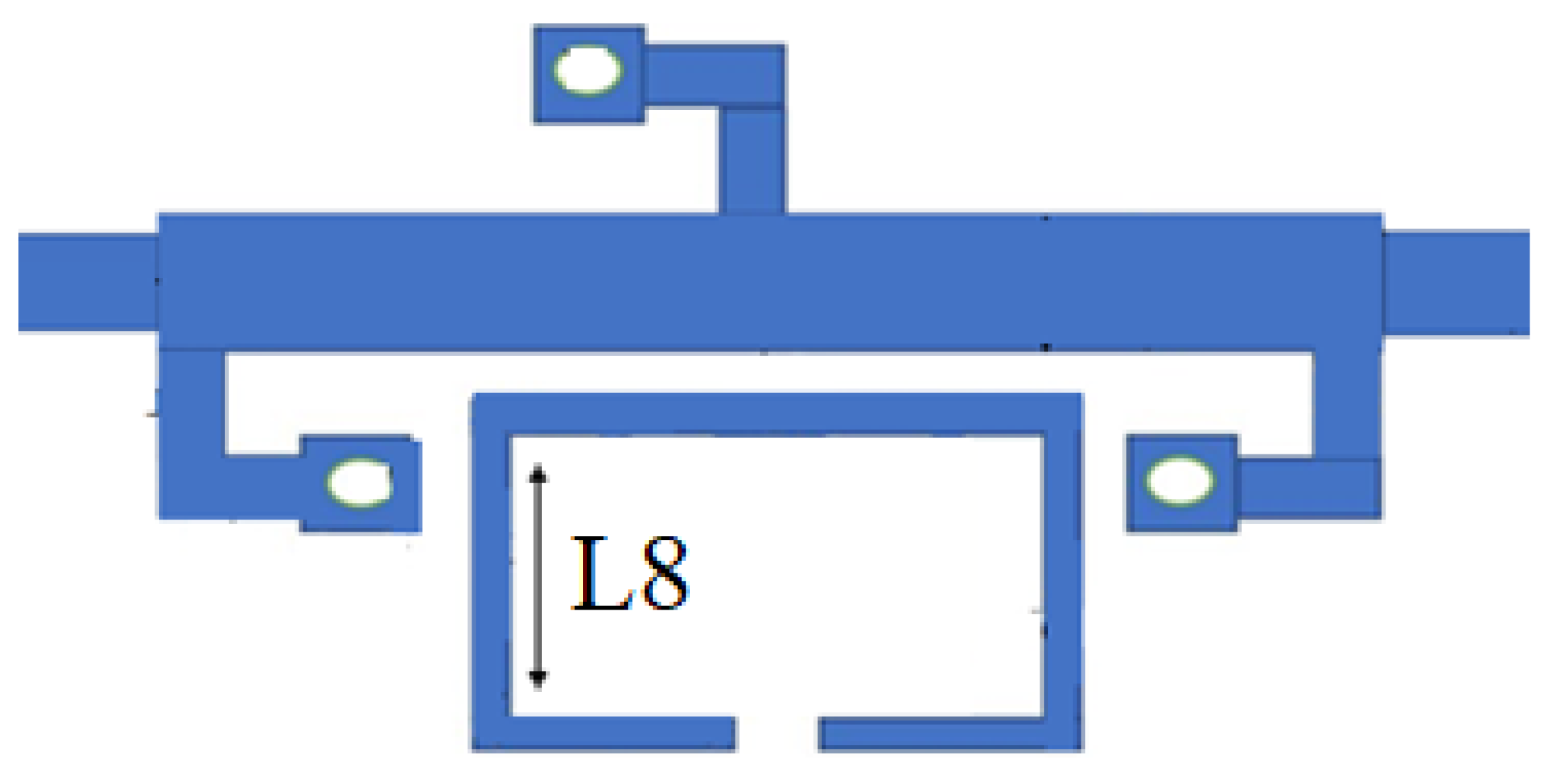
2. Design and Analysis of the SUWB-BPF
3. Operational Principle of the SUWB-BPF with In-Band Frequency Suppression
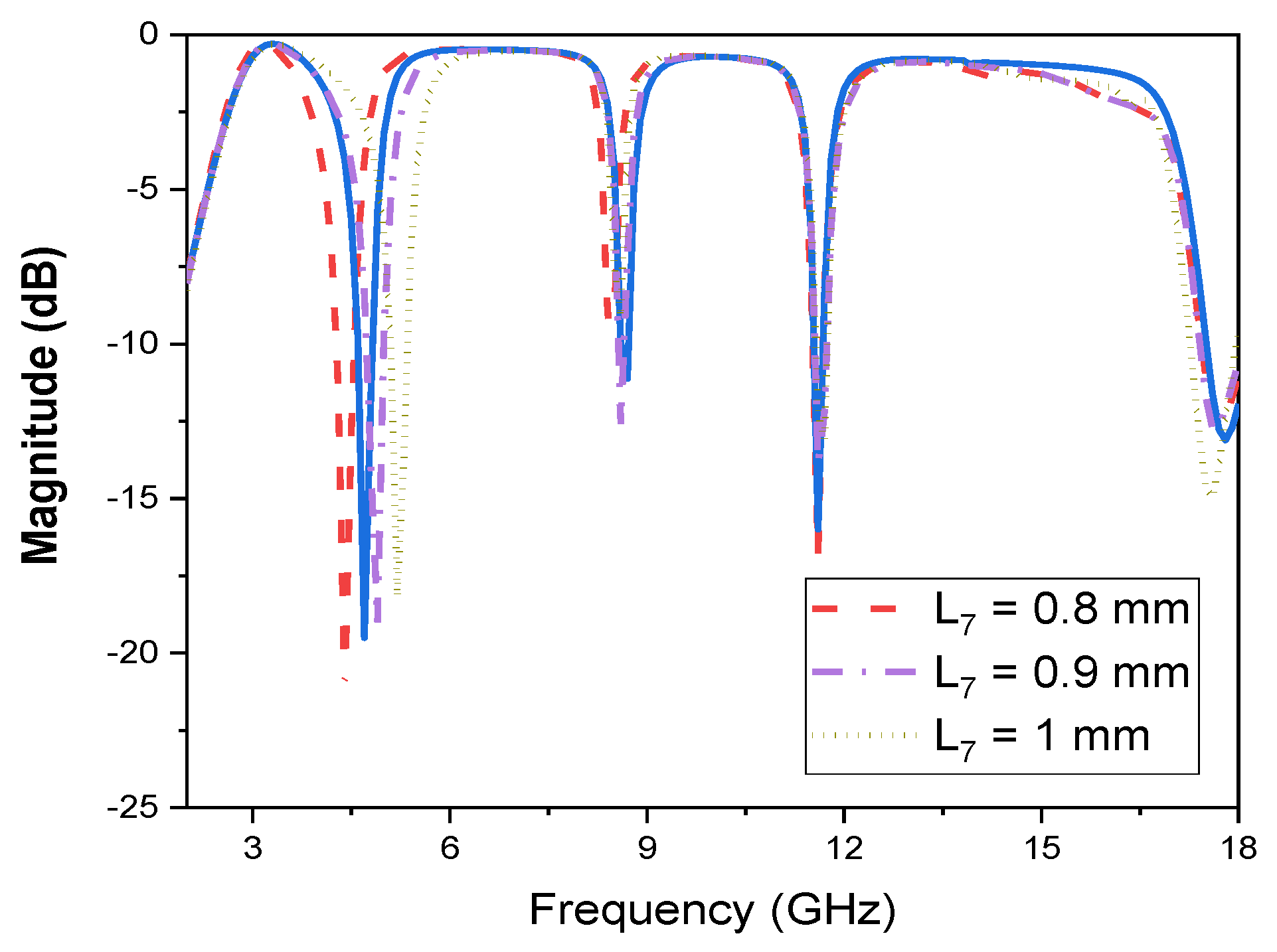
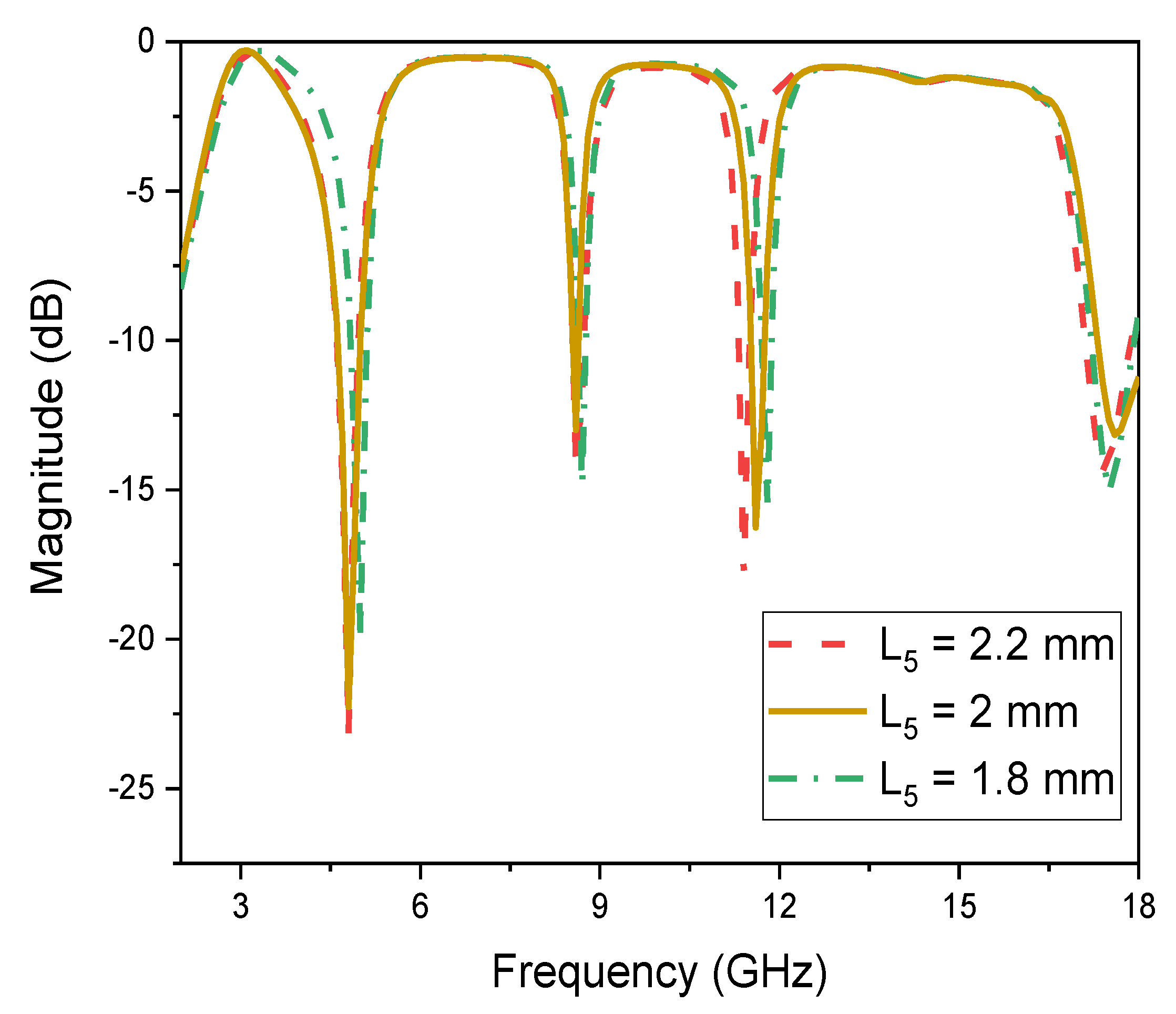
4. Proposed Filter Architecture and Determination of Stopband Frequencies
5. Measured and Experimental Results
6. Conclusions
Author Contributions
Funding
Data Availability Statement
Conflicts of Interest
References
- Bandyopadhyay; Anjan; Sarkar, P.; Ghatak, R. A Bandwidth Reconfigurable Bandpass Filter for Ultra-Wideband and Wideband Applications. IEEE Trans. Circuits Syst. II Express Briefs 2022, 13, 2747–2751. [Google Scholar]
- Ramkumar, S.; Rani, R.B. Compact reconfigurable bandpass filter using quarter wavelength stubs for ultra-wideband applications. AEU Int. J. Electron. Commun. 2022, 151, 154219. [Google Scholar] [CrossRef]
- Basit, A.; Daraz, A.; Khan, M.I.; Saqib, N.; Zhang, G. Design, Modeling, and Implementation of Dual Notched UWB Bandpass Filter Employing Rectangular Stubs and Embedded L-Shaped Structure. Fractal Fract. 2023, 7, 112. [Google Scholar] [CrossRef]
- Zhou, C.X.; Guo, P.P.; Zhou, K.; Wu, W. Design of a compact UWB filter with high selectivity and super wide stopband. IEEE Microw. Wireless Compon. Lett. 2017, 27, 636–638. [Google Scholar] [CrossRef]
- Zhou, J.; Rao, Y.; Yang, D.; Qian, H.J.; Luo, X. Compact Wideband BPF With Wide Stopband Using Substrate Integrated Defected Ground Structure. IEEE Microw. Wirel. Components Lett. 2021, 31, 353–356. [Google Scholar] [CrossRef]
- Xu, J. Compact Quasi-Elliptic Response Wideband Bandpass Filter With Four Transmission Zeros. IEEE Microw. Wirel. Components Lett. 2015, 25, 169–171. [Google Scholar] [CrossRef]
- Iqubal, A.; Abdulla, P. Bandpass filter based on asymmetric funnel shaped resonators with ultra wide upper stopband characteristics. AEU Int. J. Electron. Commun. 2020, 116, 153062. [Google Scholar] [CrossRef]
- Ali Kursad, G.; Dogan, E.; Gorur, A. Quintuple-mode wideband bandpass filter based on stub-loaded circular resonator. Int. J. RF Microw. Comput.-Aided Eng. 2022, 32, e22927. [Google Scholar]
- Zhang, X.; Liu, S.; Wang, L.; Yu, Q.; Lou, J. Design and Analysis of Ultra-wideband and Miniaturized Bandpass Filter Based on Spoof Surface Plasmon Polaritons. Plasmonics 2022, 17, 789–797. [Google Scholar] [CrossRef]
- Wang, C.-H.; Shi, X.-M. Miniaturized tri-notched wideband bandpass filter with ultrawide upper stopband suppression. Sci. Rep. 2021, 11, 13004. [Google Scholar] [CrossRef]
- Widaa, A.; You, C.J.; Awad, M.; Cai, J. Compact Wideband Bandpass Filter Using Miniaturized Staircase Interdigital Resonators. In Proceedings of the 2020 50th European Microwave Conference (EuMC), Utrecht, The Netherlands, 12–14 January 2021. [Google Scholar] [CrossRef]
- Sun, J.; Li, G.R. A balanced ultra-wideband bandpass filter based on H-type sandwich slotline. Int. J. RF Microw. Comput.-Aided Eng. 2021, 31, e22611. [Google Scholar] [CrossRef]
- Razzaz, F.; Saeed, S.M.; Alkanhal, M.A.S. Ultra-Wideband Bandpass Filters Using Tapered Resonators. Appl. Sci. 2022, 12, 3699. [Google Scholar] [CrossRef]
- Jamsai, M.; Angkawisittpan, N.; Nuan-On, A. Design of a Compact Ultra-Wideband Bandpass Filter Using Inductively Compensated Parallel-Coupled Lines. Electronics 2021, 10, 2575. [Google Scholar] [CrossRef]
- Ansoft Corporation. Ansoft HFSS (Version 13). Available online: https://www.ansys.com/products/electronics/ansys-hfss (accessed on 7 April 2023).
- Wang, C.-H.; Lin, Y.-S.; Chen, C.H. Novel inductance-incorporated microstrip coupled-line bandpass filters with two attenuation poles. In Proceedings of the 2004 IEEE MTT-S International Microwave Symposium Digest (IEEE Cat. No.04CH37535), Fort Worth, TX, USA, 6–11 June 2004. [Google Scholar] [CrossRef]
- Hong, J.-S.; Shaman, H.; Chun, Y.-H. Dual-Mode Microstrip Open-Loop Resonators and Filters. IEEE Trans. Microw. Theory Tech. 2007, 55, 1764–1770. [Google Scholar] [CrossRef]
- Guillemin, E.A. Synthesis of Passive Networks: Theory and Methods Appropriate to the Realization and Approximation Problems; Wiley: New York, NY, USA, 1959. [Google Scholar]
- Matthaei, G.L.; Young, L.; Jones, E.M.T. Microwave Filters, Impedance-Matching Networks, and Coupling Structures; Artech House Books: New York, NY, USA, 1980. [Google Scholar]
- Litvintsev, S.N.; Zakharov, A.V. Analysis of Dual-mode Resonators from Transmission Line Segments. Radioelectron. Commun. Syst. 2022, 65, 186–199. [Google Scholar] [CrossRef]
- Li, Q.; Liang, C.-H.; Wen, H.-B.; Wu, G.-C. Compact planar ultra-wideband (UWB) bandpass filter with notched band. In Proceedings of the 2009 Asia Pacific Microwave Conference, Singapore, 7–10 December 2009; pp. 257–260. [Google Scholar] [CrossRef]
- Basit, A.; Khattak, M.I.; Sebak, A.R.; Qazi, A.B.; Telba, A.A. Design of a compact microstrip triple independently controlled pass bands filter for GSM, GPS and WiFi applications. IEEE Access 2020, 8, 77156–77163. [Google Scholar] [CrossRef]
- Basit, A.; Khattak, M.I. Designing Modern Compact Microstrip Planar Quadband Bandpass Filter for Hand Held Wireless Applications. Frequenz 2020, 74, 219–227. [Google Scholar] [CrossRef]
- Pozar, D.M. Microwave Engineering, 3rd ed.; Wiley: New York, NY, USA, 2003. [Google Scholar]
- Ali, E.M.; Awan, W.A.; Naqvi, S.I.; Alzaidi, M.S.; Alzahrani, A.; Elkamchouchi, D.H.; Falcone, F.; Alharbi, T.E.A. A Low-Profile Antenna for On-Body and Off-Body Applications in the Lower and Upper ISM and WLAN Bands. Sensors 2023, 23, 709. [Google Scholar] [CrossRef]
- Ali, E.M.; Awan, W.A.; Alizaidi, M.S.; Alzahrani, A.; Elkamchouchi, D.H.; Falcone, F.; Ghoneim, S.S.M. A Shorted Stub Loaded UWB Flexible Antenna for Small IoT Devices. Sensors 2023, 23, 748. [Google Scholar] [CrossRef]
- Hussain, M.; Awan, W.A.; Alzaidi, M.S.; Hussain, N.; Ali, E.M.; Falcone, F. Metamaterials and Their Application in the Performance Enhancement of Reconfigurable Antennas: A Review. Micromachines 2023, 14, 349. [Google Scholar] [CrossRef]
- Zaidi, A.; Awan, W.A.; Ghaffar, A.; Alzaidi, M.S.; Alsharef, M.; Elkamchouchi, D.H.; Ghoneim, S.S.M.; Alharbi, T.E.A. A Low Profile Ultra-Wideband Antenna with Reconfigurable Notch Band Characteristics for Smart Electronic Systems. Micromachines 2022, 13, 1803. [Google Scholar] [CrossRef] [PubMed]
- Basit, A.; Khattak, M.I.; Nebhen, J.; Jan, A.; Ahmad, G. Investigation of external quality factor and coupling coefficient for a novel SIR based microstrip tri-band bandpass filter. PLoS ONE 2021, 16, e0258386. [Google Scholar] [CrossRef] [PubMed]
- El Bakali, H.E.; Elftouh, H.; Farkhsi, A.; Zakriti, A.; El Ouahabi, M. Design of a Super Compact UWB Filter Based on Hybrid Technique with a Notch Band Using Open Circuited Stubs. Adv. Electromagn. 2020, 9, 39–46. [Google Scholar] [CrossRef]
- Kamma, A.; Das, R.; Bhatt, D.; Mukherjee, J. Multi Mode Resonators Based Triple Band Notch UWB Filter. IEEE Microw. Wirel. Components Lett. 2017, 27, 120–122. [Google Scholar] [CrossRef]
- Kumar, S.; Gupta, R.D.; Parihar, M.S. Multiple Band Notched Filter Using C-Shaped and E-Shaped Resonator for UWB Applications. IEEE Microw. Wirel. Compon. Lett. 2016, 26, 340–342. [Google Scholar] [CrossRef]
- Xiao, Y.; Li, G.; Chen, B.; Jiang, Q.; Song, Y. Band-notched ultra-wideband bandpass filter with broad stopband. IEEE Asia-Pac. Int. Symp. Electromagn. Compat. (APEMC) 2022, 548–550. [Google Scholar] [CrossRef]
- Bohra, H.; Ghosh, A.; Bhaskar, A.; Sharma, A. A Miniaturized Notched Band Microstrip Wideband Filter with Hybrid Defected Ground Structure Technique. In Proceedings of the 2020 Third International Conference on Smart Systems and Inventive Technology (ICSSIT), Tirunelveli, India, 20–22 August 2020; pp. 745–750. [Google Scholar] [CrossRef]
- Ranjan, P.; Kishore, N.; Dwivedi, V.K.; Upadhyay, G.; Tripathi, V.S. UWB filter with controllable notch band and higher stop band transmission zero using open stub in inverted T-shaped resonator. In Proceedings of the 2017 IEEE Asia Pacific Microwave Conference (APMC), Kuala Lumpar, Malaysia, 13–16 November 2017; pp. 817–820. [Google Scholar] [CrossRef]
- Ghazali, A.N.; Sazid, M.; Pal, S. A dual notched band UWB-BPF based on microstrip-to-short circuited CPW transition. Int. J. Microw. Wirel. Technol. 2018, 10, 794–800. [Google Scholar] [CrossRef]
- Kavosi, M.; Nourinia, J.; Ghobadi, C.; Bazdar, A.; Mohammadi, B. A compact UWB ring resonator BPF with double notched bands. In Proceedings of the 2017 IEEE 4th International Conference on Knowledge-Based Engineering and Innovation (KBEI), Tehran, Iran, 22 December 2017; pp. 69–71. [Google Scholar]
- Sazid, M.; Raghava, N. Planar UWB-bandpass filter with multiple passband transmission zeros. AEU Int. J. Electron. Commun. 2021, 134, 153711. [Google Scholar] [CrossRef]


| L | 22.5 | W | 3.2 | L1 | 4 | L2 | 1 |
| L3 | 1.5 | L4 | 9 | L5 | 2 | L6 | 6 |
| W1 | 1 | L8 | 2.9 | L9 | 1.2 | L7 | 0.8 |
| W2 | 0.3 | W3 | 1.5 | W4 | 0.5 | S | 0.1 |
| R1 | 0.55 | R2 | 0.3 | PCB height | 1.5 | PCB | RO-4350 |
| ϵr | 3.6 | tan δ | 0.0003 | Wf | 3.1 |
| Serial No. | Design Equation | Design Resonator Model | Theoretical Results | Simulated Results |
|---|---|---|---|---|
| 1st stopband |  | 5.5 GHz | 4.9 GHz | |
| 2nd stopband |  | 8.1 GHz | 8.3 GHz | |
| 3rd stopband |  | 10.8 GHz | 11.5 GHz |
| Serial No. | Insertion Loss | Bandwidth (MHz) | Rejection Level |
|---|---|---|---|
| 1ststopband | <0.5 dB | 300 | −20 dB |
| 2ndstopband | <0.5 dB | 290 | −15 dB |
| 3rdstopband | <0.5 dB | 170 | −19.3 dB |
| Serial No. | Theoretical Results | Simulated Results | Measured Results |
|---|---|---|---|
| 1ststopband | 5.5 GHz | 4.9 GHz | 4.83 GHz |
| 2ndstopband | 8.1 GHz | 8.3 GHz | 8.51 GHz |
| 3rdstopband | 10.8 GHz | 11.5 GHz | 11.69 GHz |
| S1 (mm) | 1st Band (GHz) | 2nd Band (GHz) | 3rd Band (GHz) |
|---|---|---|---|
| 0.08 | 0.08 | 0.06 | 0.04 |
| 0.09 | 0.065 | 0.058 | 0.038 |
| 0.1 | 0.055 | 0.048 | 0.031 |
| 0.2 | 0.03 | 0.01 | 0.021 |
| Ref. No. | Passband (GHz) | FBW (%) | IL/RL (dB) | C.F/BW (GHz) |
|---|---|---|---|---|
| [31] | 3.3–10.7 | 105.7 | 0.9/15 | 4.4, 5.5, 7.6 |
| [32] | 3.1–10.6 | 117.0 | 1.25/>16 | 3.6, 5.2, 8.4 |
| [33] | 3.3–9.7 | 104 | 0.3/29 | 7.3 |
| [34] | 3.3–10.6 | 105 | <0.5/14 | 8.95 |
| [35] | 3.1–11 | 112 | 0.66/35 | 6 |
| [36] | 3–10.9 | 110 | 0.9/>15 | 5.96, 8.15 |
| [37] | 3.58–10.07 | 95.1 | <1.2/>15 | 5.53, 8.1 |
| [38] | 3.25–10.73 | 106 | 0.52/>19 | 5.6, 6.4, 8.03 |
| This work | 2.9–16.85 | 141.1 | <0.4/>15 | 4.9, 8.3, 11.5 |
Disclaimer/Publisher’s Note: The statements, opinions and data contained in all publications are solely those of the individual author(s) and contributor(s) and not of MDPI and/or the editor(s). MDPI and/or the editor(s) disclaim responsibility for any injury to people or property resulting from any ideas, methods, instructions or products referred to in the content. |
© 2023 by the authors. Licensee MDPI, Basel, Switzerland. This article is an open access article distributed under the terms and conditions of the Creative Commons Attribution (CC BY) license (https://creativecommons.org/licenses/by/4.0/).
Share and Cite
Zhang, G.; Basit, A.; Khan, M.I.; Daraz, A.; Saqib, N.; Zubir, F. Multi Frequency Controllable In-Band Suppressions in a Broad Bandwidth Microstrip Filter Design for 5G Wi-Fi and Satellite Communication Systems Utilizing a Quad-Mode Stub-Loaded Resonator. Micromachines 2023, 14, 866. https://doi.org/10.3390/mi14040866
Zhang G, Basit A, Khan MI, Daraz A, Saqib N, Zubir F. Multi Frequency Controllable In-Band Suppressions in a Broad Bandwidth Microstrip Filter Design for 5G Wi-Fi and Satellite Communication Systems Utilizing a Quad-Mode Stub-Loaded Resonator. Micromachines. 2023; 14(4):866. https://doi.org/10.3390/mi14040866
Chicago/Turabian StyleZhang, Guoqiang, Abdul Basit, Muhammad Irshad Khan, Amil Daraz, Najmus Saqib, and Farid Zubir. 2023. "Multi Frequency Controllable In-Band Suppressions in a Broad Bandwidth Microstrip Filter Design for 5G Wi-Fi and Satellite Communication Systems Utilizing a Quad-Mode Stub-Loaded Resonator" Micromachines 14, no. 4: 866. https://doi.org/10.3390/mi14040866
APA StyleZhang, G., Basit, A., Khan, M. I., Daraz, A., Saqib, N., & Zubir, F. (2023). Multi Frequency Controllable In-Band Suppressions in a Broad Bandwidth Microstrip Filter Design for 5G Wi-Fi and Satellite Communication Systems Utilizing a Quad-Mode Stub-Loaded Resonator. Micromachines, 14(4), 866. https://doi.org/10.3390/mi14040866