Concurrently Fabricating Precision Meso- and Microscale Cross-Scale Arrayed Metal Features and Components by Using Wire-Anode Scanning Electroforming Technique
Abstract
:1. Introduction
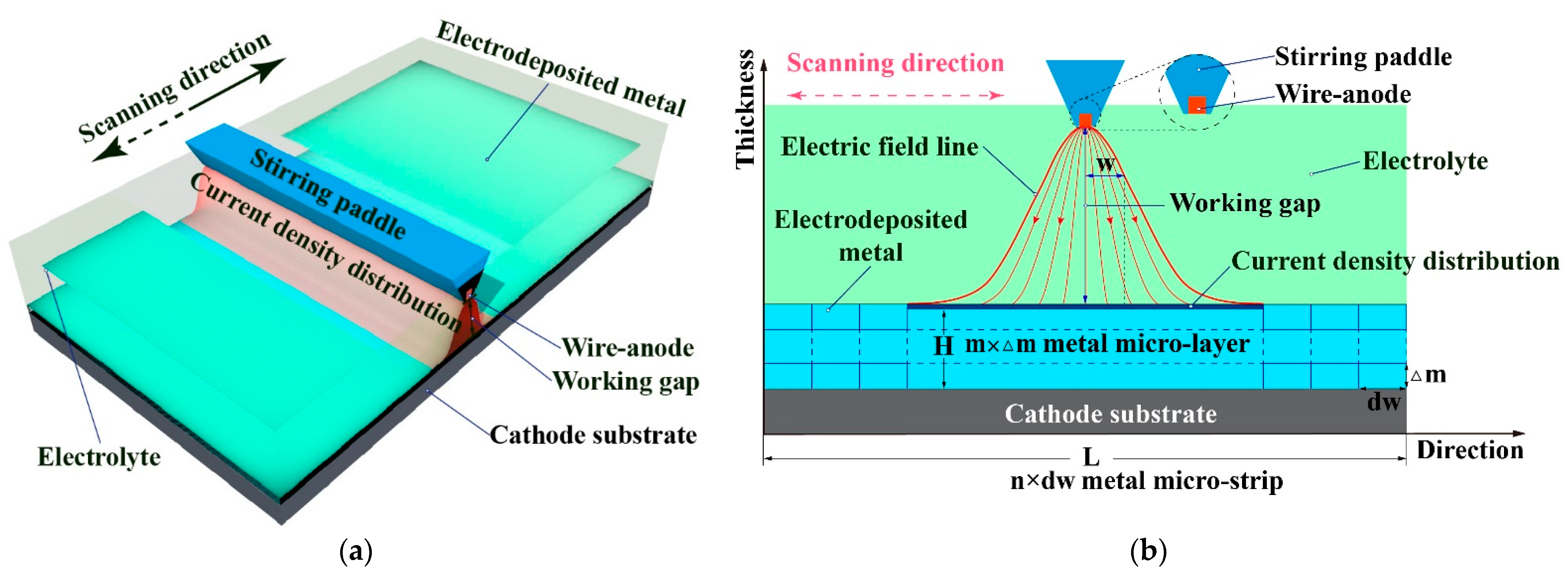
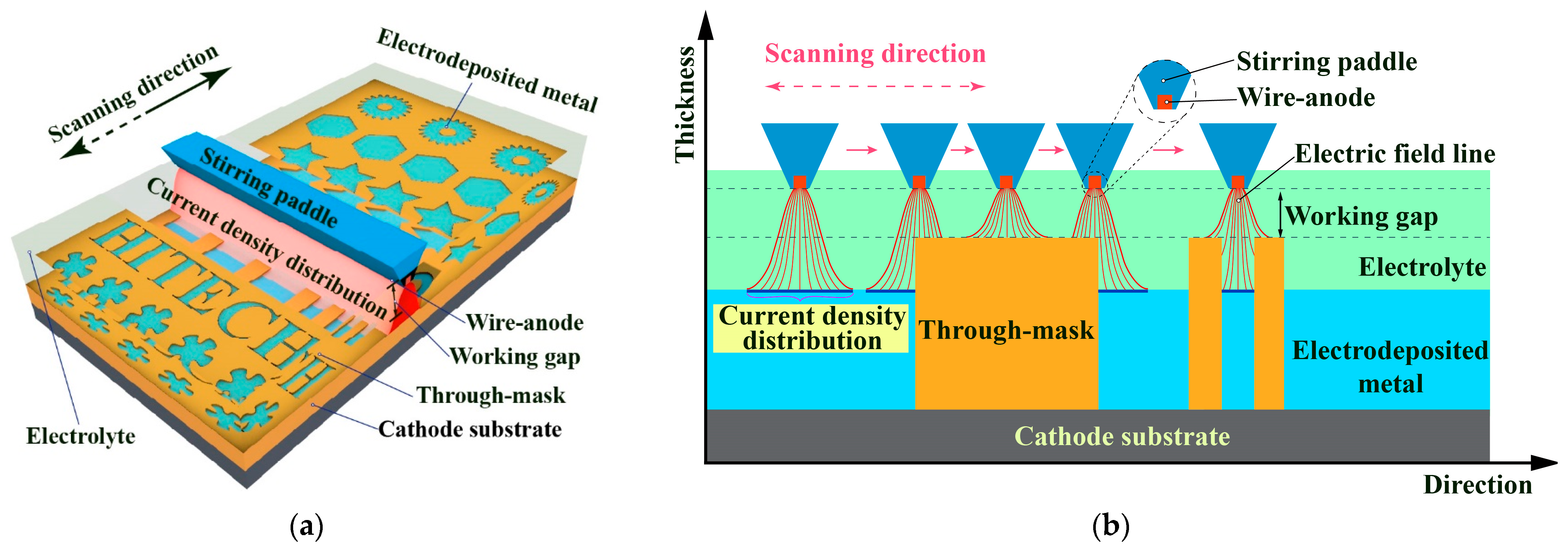
2. Working Scheme of Wire-Anode Scanning Electroforming
3. Simulation of Electric and Flow Fields during WAS-EF
3.1. Modeling and Conditions
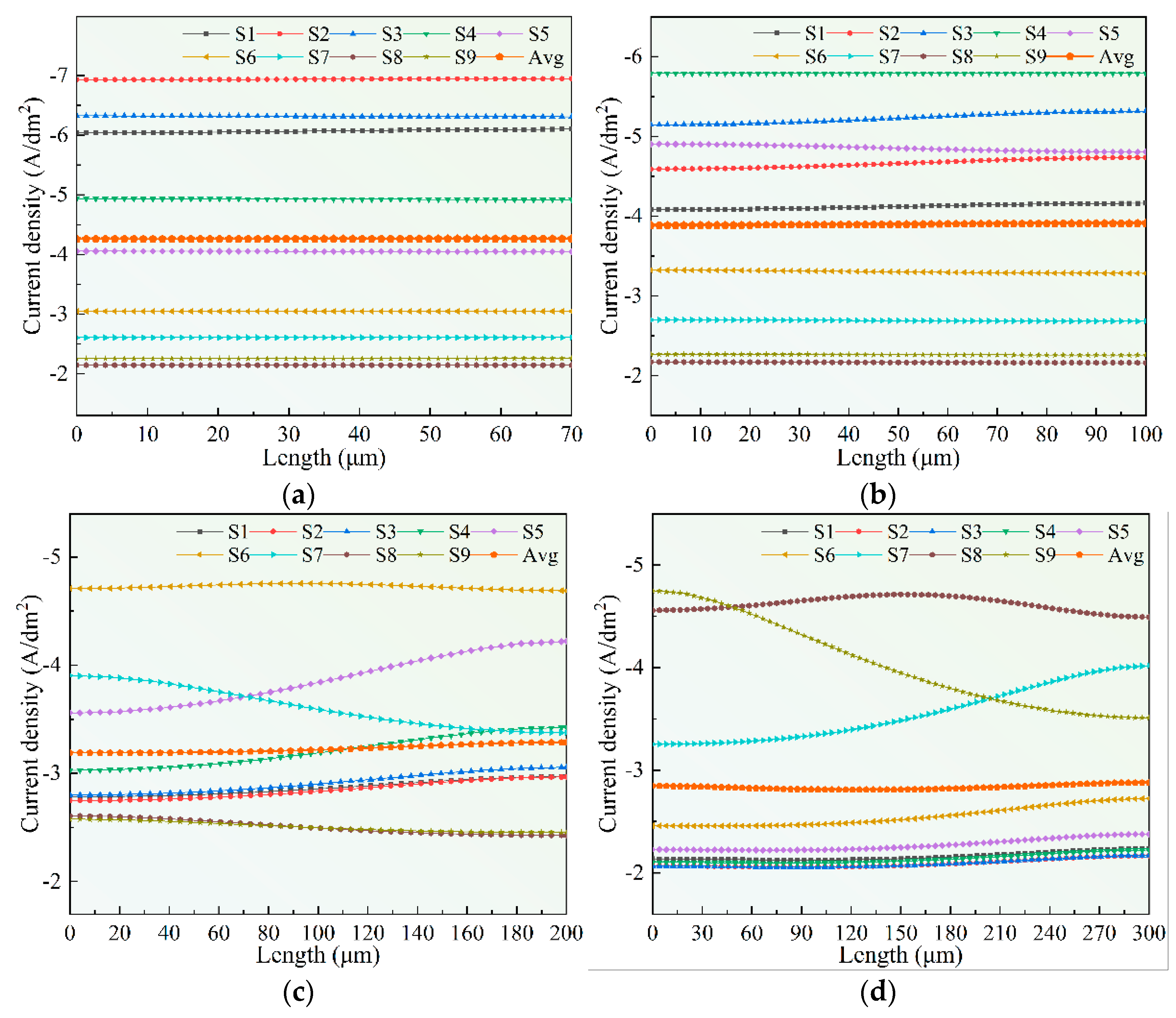
3.2. Electric Field Distribution in the Cathode Region
3.3. Distribution of Flow Field in the Cathode Region
4. Experimental Study
4.1. Experimental Setup and Materials
4.2. Surface Morphologies and Geometrical Dimension Accuracy Characterization
5. Results and Discussion
5.1. Surface Morphology Analysis of Parts
5.2. Characteristic Analysis of Single Part
5.3. Characteristic Analysis of Part Arrays
5.4. Parametric Analysis of Thickness Uniformity of Electroforming Parts
6. Conclusions
- (1)
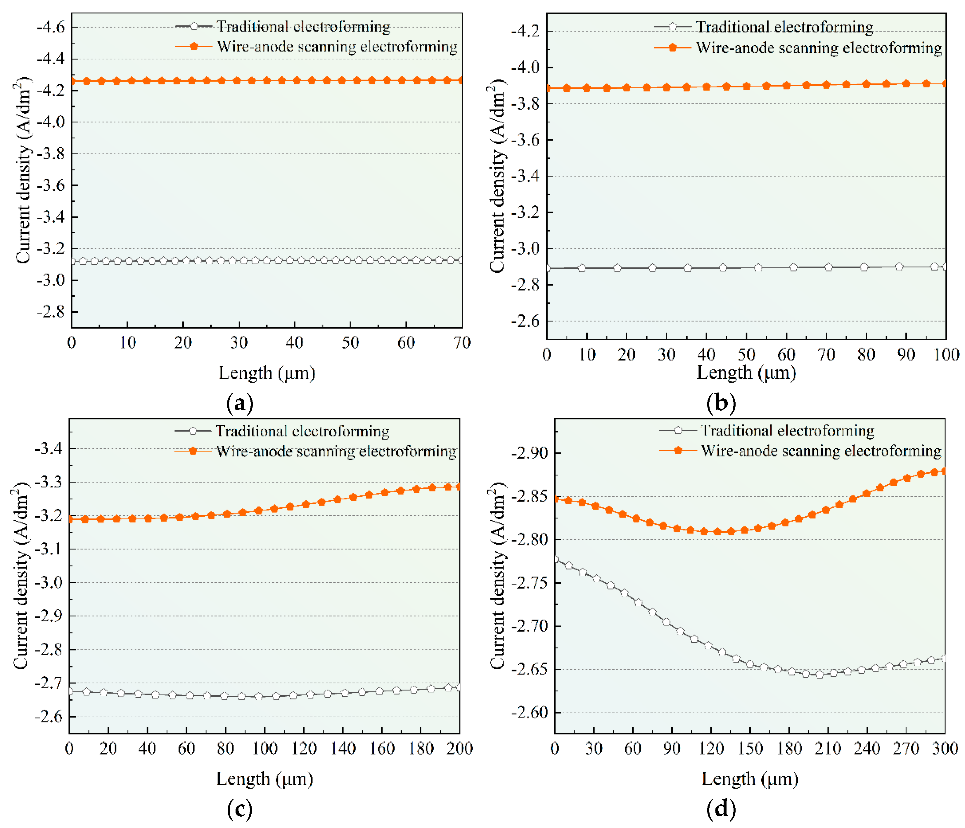
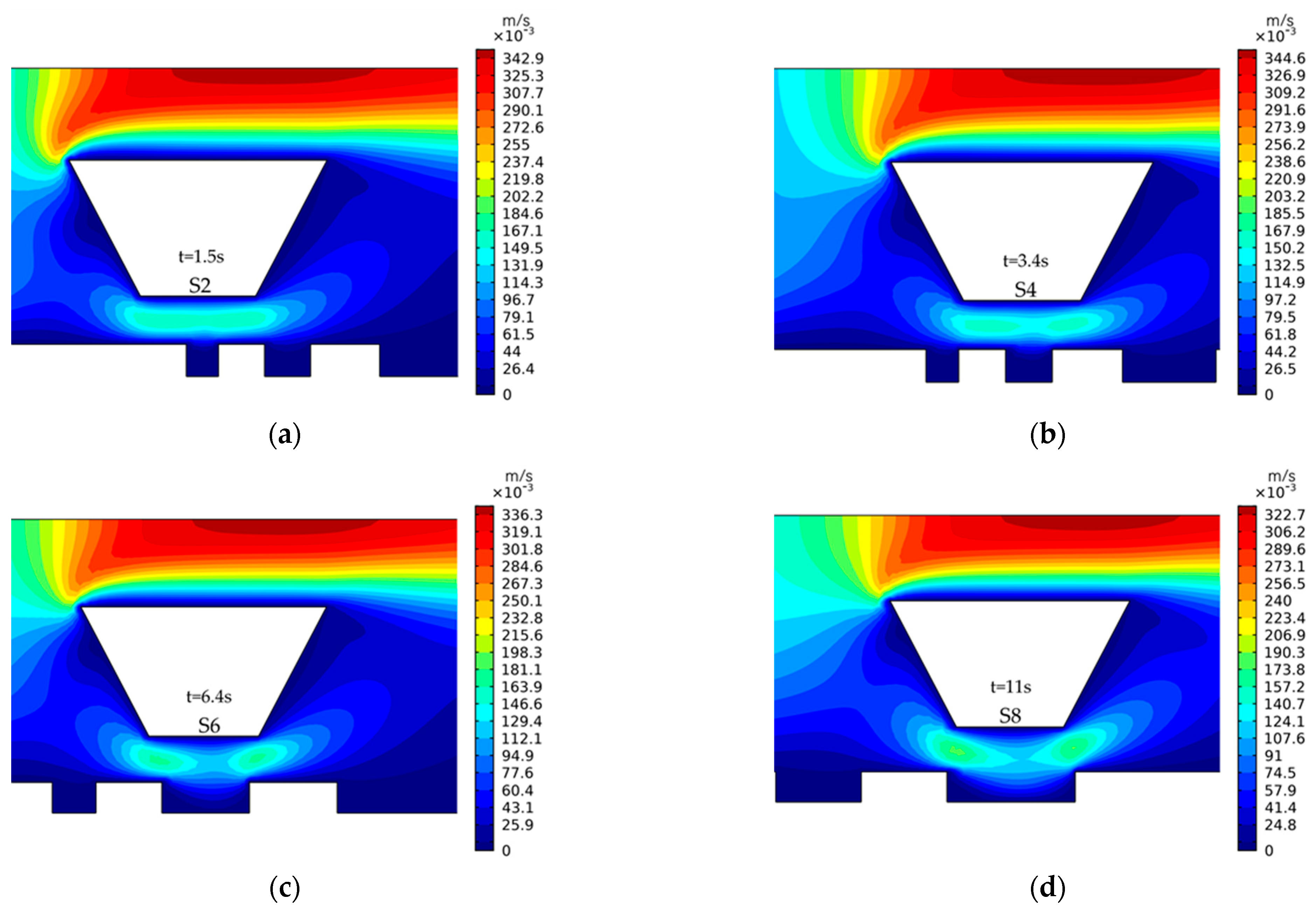
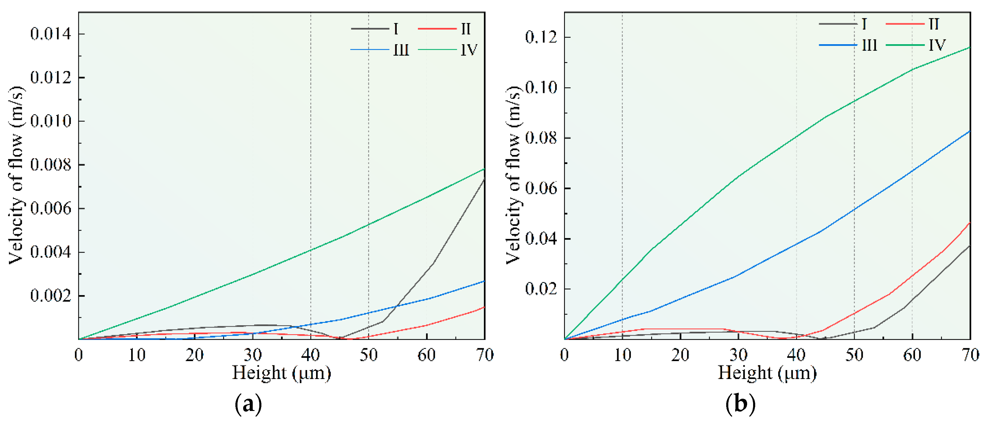
- Through numerical simulation, it can be concluded that the eddy current generated by a stirring paddle motion can affect the flow field in the micropore, resulting in a better mass transfer effect on the cathode surface. On the other hand, by stacking electric fields, it can be seen that the current density is higher and the distribution is more uniform in the mode of wire-anode scanning electroforming.
- (2)
- The results show that the uniformity of components decreases with the increase in the working gap. When the machining voltage is high or low, the surface quality of components is not ideal. Under the optimized working gap and machining voltage, components with better uniformity can be obtained.
- (3)
- Compared with the traditional electroforming technique, the thickness uniformity of wire-anode scanning electroforming is improved by 15.5% on average for the preparation of single-scale components, and 11.4% for the preparation of multi-scale component arrays.
Author Contributions
Funding
Data Availability Statement
Acknowledgments
Conflicts of Interest
References
- Ehmann, K.F.; DeVor, R.E.; Kapoor, S.G. PL-2 Micro/Meso-Scale Mechanical Manufacturing: Opportunities and Challenges. JSME/ASME Int. Conf. Mater. Process. 2002, 1, 6–13. [Google Scholar] [CrossRef]
- Chaubey, S.K.; Jain, N.K. State-of-Art Review of Past Research on Manufacturing of Meso and Micro Cylindrical Gears. Precis. Eng. 2018, 51, 702–728. [Google Scholar] [CrossRef]
- Seo, H.; Kishimoto, M.; Nakagawa, T.; Iwai, H.; Yoshida, H. Mechanism of Improved Electrochemical Performance of Anode-Supported Solid Oxide Fuel Cells by Mesostructural Modification of Electrode–Electrolyte Interface. J. Power Sources 2021, 506, 230107. [Google Scholar] [CrossRef]
- Lee, Y.-S.; Bhattacharjee, N.; Folch, A. 3D-Printed Quake-Style Microvalves and Micropumps. Lab Chip 2018, 18, 1207–1214. [Google Scholar] [CrossRef] [PubMed]
- Im, S.B.; Uddin, M.J.; Jin, G.J.; Shim, J.S. A Disposable On-Chip Microvalve and Pump for Programmable Microfluidics. Lab Chip 2018, 18, 1310–1319. [Google Scholar] [CrossRef]
- Van Lith, R.; Baker, E.; Ware, H.; Yang, J.; Farsheed, A.C.; Sun, C.; Ameer, G. 3D-Printing Strong High-Resolution Antioxidant Bioresorbable Vascular Stents. Adv. Mater. Technol. 2016, 1, 1600138. [Google Scholar] [CrossRef]
- O’Toole, L.; Kang, C.-W.; Fang, F.-Z. Precision Micro-Milling Process: State of the Art. Adv. Manuf. 2021, 9, 173–205. [Google Scholar] [CrossRef]
- Hasan, M.; Zhao, J.; Jiang, Z. A Review of Modern Advancements in Micro Drilling Techniques. J. Manuf. Process. 2017, 29, 343–375. [Google Scholar] [CrossRef]
- Bachus, K.J.; Mats, L.; Choi, H.W.; Gibson, G.T.T.; Oleschuk, R.D. Fabrication of Patterned Superhydrophobic/Hydrophilic Substrates by Laser Micromachining for Small Volume Deposition and Droplet-Based Fluorescence. ACS Appl. Mater. Interfaces 2017, 9, 7629–7636. [Google Scholar] [CrossRef]
- Li, P.; Chen, S.; Dai, H.; Yang, Z.; Chen, Z.; Wang, Y.; Chen, Y.; Peng, W.; Shan, W.; Duan, H. Recent Advances in Focused Ion Beam Nanofabrication for Nanostructures and Devices: Fundamentals and Applications. Nanoscale 2021, 13, 1529–1565. [Google Scholar] [CrossRef]
- Buchnev, O.; Grant-Jacob, J.A.; Eason, R.W.; Zheludev, N.I.; Mills, B.; MacDonald, K.F. Deep-Learning-Assisted Focused Ion Beam Nanofabrication. Nano Lett. 2022, 22, 2734–2739. [Google Scholar] [CrossRef]
- Zou, Z.; Guo, Z.; Huang, Q.; Yue, T.; Liu, J.; Chen, X. Precision EDM of Micron-Scale Diameter Hole Array Using in-Process Wire Electro-Discharge Grinding High-Aspect-Ratio Microelectrodes. Micromachines 2021, 12, 17. [Google Scholar] [CrossRef]
- Zhan, D.; Han, L.; Zhang, J.; Shi, K.; Zhou, J.-Z.; Tian, Z.-W.; Tian, Z.-Q. Confined Chemical Etching for Electrochemical Machining with Nanoscale Accuracy. Acc. Chem. Res. 2016, 49, 2596–2604. [Google Scholar] [CrossRef]
- Schuster, R.; Kirchner, V.; Allongue, P.; Ertl, G. Electrochemical Micromachining. Science 2000, 289, 98–101. [Google Scholar] [CrossRef]
- Wei, W.; Pingmei, M.; Xinmin, Z.; Xinchao, L.; Yunyan, Z.; Shen, N.; Sansan, A. Additive Manufacturing of Three-Dimensional Intricate Microfeatures by Electrolyte-Column Localized Electrochemical Deposition. Addit. Manuf. 2022, 50, 102582. [Google Scholar] [CrossRef]
- Hossain Bhuiyan, M.E.; Moreno, S.; Wang, C.; Minary-Jolandan, M. Interconnect Fabrication by Electroless Plating on 3D-Printed Electroplated Patterns. ACS Appl. Mater. Interfaces 2021, 13, 19271–19281. [Google Scholar] [CrossRef]
- Kimura, M.; Yamagiwa, H.; Asakawa, D.; Noguchi, M.; Kurashina, T.; Fukawa, T.; Shirai, H. Site-Selective Electroless Nickel Plating on Patterned Thin Films of Macromolecular Metal Complexes. ACS Appl. Mater. Interfaces 2010, 2, 3714–3717. [Google Scholar] [CrossRef]
- Chen, P.; van Veldhoven, E.; Sanford, C.A.; Salemink, H.W.M.; Maas, D.J.; Smith, D.A.; Rack, P.D.; Alkemade, P.F.A. Nanopillar Growth by Focused Helium Ion-Beam-Induced Deposition. Nanotechnology 2010, 21, 455302. [Google Scholar] [CrossRef]
- Ning, B.; Xia, T.; Tong, Z.-X.; He, Y.-L. Experimental and Numerical Studies of Tungsten Line Growth in Laser Chemical Vapor Deposition. Int. J. Heat Mass Transf. 2019, 140, 564–578. [Google Scholar] [CrossRef]
- Yang, H.; Kang, S.-W. Improvement of Thickness Uniformity in Nickel Electroforming for the LIGA Process. Int. J. Adv. Manuf. Technol. 2000, 40, 1065–1072. [Google Scholar] [CrossRef]
- Qian, S.; Ji, F.; Qu, N.; Li, H. Improving the Localization of Surface Texture by Electrochemical Machining with Auxiliary Anode. Mater. Manuf. Process. 2014, 29, 1488–1493. [Google Scholar] [CrossRef]
- Zhao, M.; Du, L.; Wei, Z.; Du, C.; Liu, X.; Ji, X. Fabrication of Metal Microfluidic Chip Mold with Coplanar Auxiliary Cathode in the Electroforming Process. J. Micromech. Microeng. 2018, 29, 025002. [Google Scholar] [CrossRef]
- Ishizuka, N.; Yamada, T.; Izui, K.; Nishiwaki, S. Topology Optimization for Unifying Deposit Thickness in Electroplating Process. Struct. Multidiscipl. Optim. 2020, 62, 1767–1785. [Google Scholar] [CrossRef]
- Xiang, J.; Chen, P.; Wang, Y.; Zeng, C.; Yang, W.; Li, J.; Xu, Y. Numerical Simulation of Optimizing Plating Uniformity of Interconnect Circuits on Printed Circuit Boards. J. Phys. Conf. Ser. 2021, 1986, 012135. [Google Scholar] [CrossRef]
- Volgin, V.M.; Lyubimov, V.V.; Gnidina, I.V.; Kabanova, T.B.; Davydov, A.D. Effect of Anode Shape on Uniformity of Electrodeposition onto Resistive Substrates. Electrochim. Acta 2017, 230, 382–390. [Google Scholar] [CrossRef]
- Fukukawa, M.; Tong, L. Effect of Mass Flow Induced by a Reciprocating Paddle on Electroplating. In Proceedings of the 2017 COMSOL Conference, Boston, MA, USA, 4–6 October 2017. [Google Scholar]
- Zhao, Y.; Qian, S.; Zhang, Y.; Wan, X.; Zhang, H. Experimental Study on Uniformity of Copper Layer with Microstructure Arrays by Electroforming. Int. J. Adv. Manuf. Technol. 2021, 114, 2019–2030. [Google Scholar] [CrossRef]
- Cao, Q.-D.; Fang, L.; Lv, J.-M.; Zhang, X.-P.; Thuy Dat, N. Effects of Pulse Reverse Electroforming Parameters on the Thickness Uniformity of Electroformed Copper Foil. Trans. Inst. Met. Finish. 2018, 96, 108–112. [Google Scholar] [CrossRef]
- Suzuki, A.; Oue, S.; Kobayashi, S.; Nakano, H. Effects of Additives on the Surface Roughness and Throwing Power of Copper Deposited from Electrorefining Solutions. Mater. Trans. 2017, 58, 1538–1545. [Google Scholar] [CrossRef]
- Chen, T.-C.; Tsai, Y.-L.; Hsu, C.-F.; Dow, W.-P.; Hashimoto, Y. Effects of Brighteners in a Copper Plating Bath on Throwing Power and Thermal Reliability of Plated Through Holes. Electrochim. Acta 2016, 212, 572–582. [Google Scholar] [CrossRef]
- Chen, Y.; He, W.; Chen, X.; Wang, C.; Tao, Z.; Wang, S.; Zhou, G.; Moshrefi-Torbati, M. Plating Uniformity of Bottom-up Copper Pillars and Patterns for IC Substrates with Additive-Assisted Electrodeposition. Electrochim. Acta 2014, 120, 293–301. [Google Scholar] [CrossRef]
- Tsai, T.-H.; Yang, H.; Chein, R. New Electroforming Technology Pressure Aid for LIGA Process. Microsyst. Technol. 2004, 10, 351–356. [Google Scholar] [CrossRef]
- Zhai, K.; Du, L.; Wang, W.; Zhu, H.; Zhao, W.; Zhao, W. Research of Megasonic Electroforming Equipment Based on the Uniformity of Electroforming Process. Ultrason. Sonochem. 2018, 42, 368–375. [Google Scholar] [CrossRef]
- Ke, J.; Su, W.; Howdle, S.M.; George, M.W.; Cook, D.; Perdjon-Abel, M.; Bartlett, P.N.; Zhang, W.; Cheng, F.; Levason, W.; et al. Electrodeposition of Metals from Supercritical Fluids. Proc. Natl. Acad. Sci. USA 2009, 106, 14768–14772. [Google Scholar] [CrossRef]
- Xiao, Y.; Ming, P.; Zhang, X.; Hou, Y.; Du, L.; Li, S.; Zhang, Y.; Song, J. Ultrahigh Strength Ultrapure Nanostructured Nickel Metal Prepared via Ultrafine Anode Scanning Electrodeposition. Mater. Des. 2022, 213, 110339. [Google Scholar] [CrossRef]
- Foias, C.; Temam, R. Gevrey Class Regularity for the Solutions of the Navier-Stokes Equations. J. Funct. Anal. 1989, 87, 359–369. [Google Scholar] [CrossRef]
- Dickinson, E.J.F.; Wain, A.J. The Butler-Volmer Equation in Electrochemical Theory: Origins, Value, and Practical Application. J. Electroanal. Chem. 2020, 872, 114145. [Google Scholar] [CrossRef]

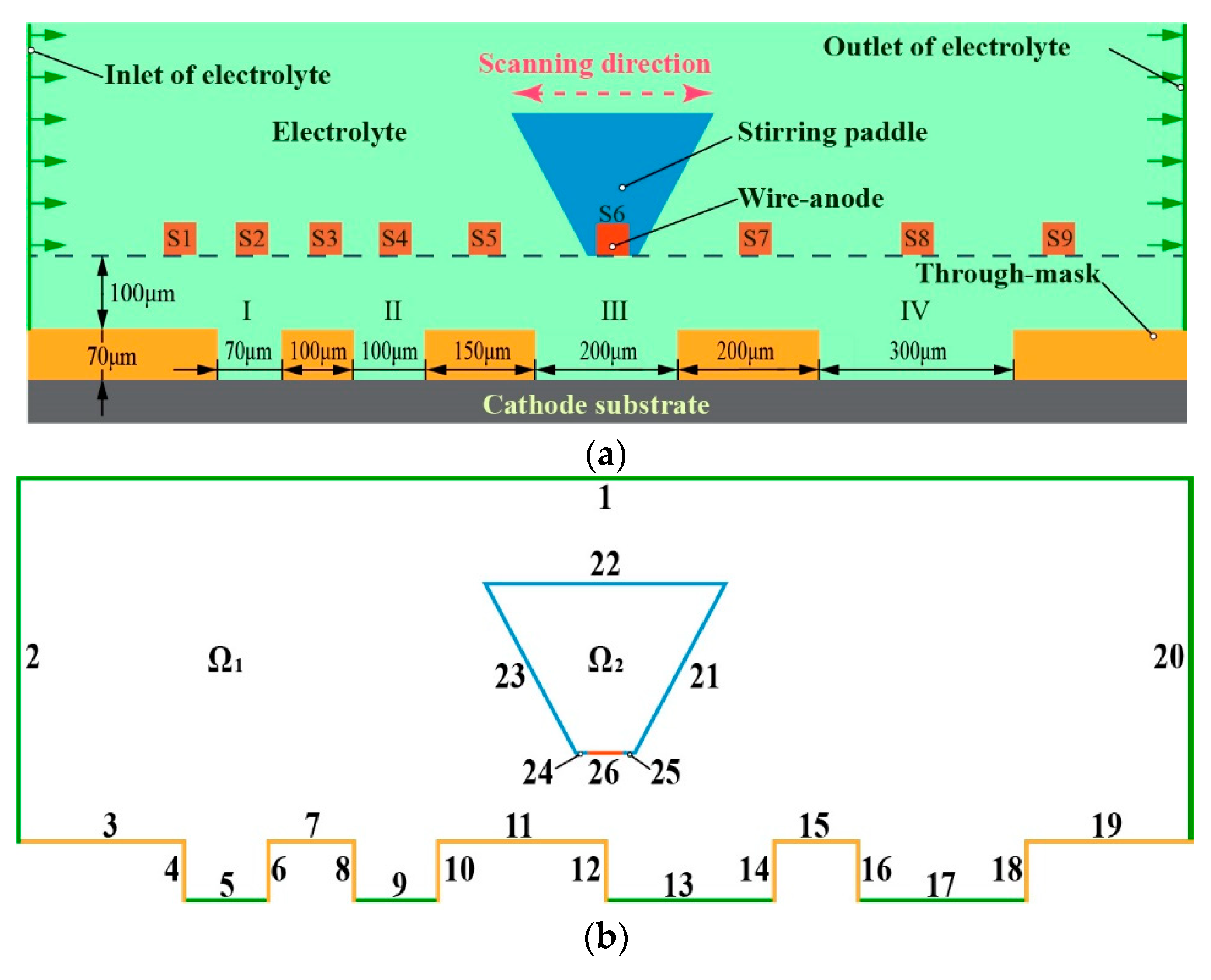



| Domain Conditions | Domain | Property |
|---|---|---|
| Electrolyte | Ω1 | ρ1 = 1.042 g/cm3; μ1 = 1.062 × 10⁻³ Pa·s σ1 = 10.3 S/m; T = 328.15 K |
| Stirring paddle | Ω2 | ρ2 = 1.18 g/cm3; E = 3.16 × 10⁹ Pa nu = 0.32 |
| Specify deformation domain | Ω2 | X = 0.00055 [m] × sin (2 × pi × t [1/s]); Y = 0 |
| Boundary Conditions | Boundary | Property |
|---|---|---|
| Electrolyte inlet | 2 | U0 = 0.1 m/s |
| Outlet | 20 | p0 = 0 Pa |
| Anode | 26 | I0 = 250 A/m2 |
| Cathode | 5, 9, 13, 17 | 0 V |
| Wall | 3–19 | Slip |
Disclaimer/Publisher’s Note: The statements, opinions and data contained in all publications are solely those of the individual author(s) and contributor(s) and not of MDPI and/or the editor(s). MDPI and/or the editor(s) disclaim responsibility for any injury to people or property resulting from any ideas, methods, instructions or products referred to in the content. |
© 2023 by the authors. Licensee MDPI, Basel, Switzerland. This article is an open access article distributed under the terms and conditions of the Creative Commons Attribution (CC BY) license (https://creativecommons.org/licenses/by/4.0/).
Share and Cite
Li, S.; Ming, P.; Zhang, J.; Zhang, Y.; Yan, L. Concurrently Fabricating Precision Meso- and Microscale Cross-Scale Arrayed Metal Features and Components by Using Wire-Anode Scanning Electroforming Technique. Micromachines 2023, 14, 979. https://doi.org/10.3390/mi14050979
Li S, Ming P, Zhang J, Zhang Y, Yan L. Concurrently Fabricating Precision Meso- and Microscale Cross-Scale Arrayed Metal Features and Components by Using Wire-Anode Scanning Electroforming Technique. Micromachines. 2023; 14(5):979. https://doi.org/10.3390/mi14050979
Chicago/Turabian StyleLi, Shicheng, Pingmei Ming, Junzhong Zhang, Yunyan Zhang, and Liang Yan. 2023. "Concurrently Fabricating Precision Meso- and Microscale Cross-Scale Arrayed Metal Features and Components by Using Wire-Anode Scanning Electroforming Technique" Micromachines 14, no. 5: 979. https://doi.org/10.3390/mi14050979
APA StyleLi, S., Ming, P., Zhang, J., Zhang, Y., & Yan, L. (2023). Concurrently Fabricating Precision Meso- and Microscale Cross-Scale Arrayed Metal Features and Components by Using Wire-Anode Scanning Electroforming Technique. Micromachines, 14(5), 979. https://doi.org/10.3390/mi14050979


