
Modeling the Impact of Phonon Scattering with Strain Effects on the Electrical Properties of MoS2 Field-Effect Transistors

Abstract
:1. Introduction
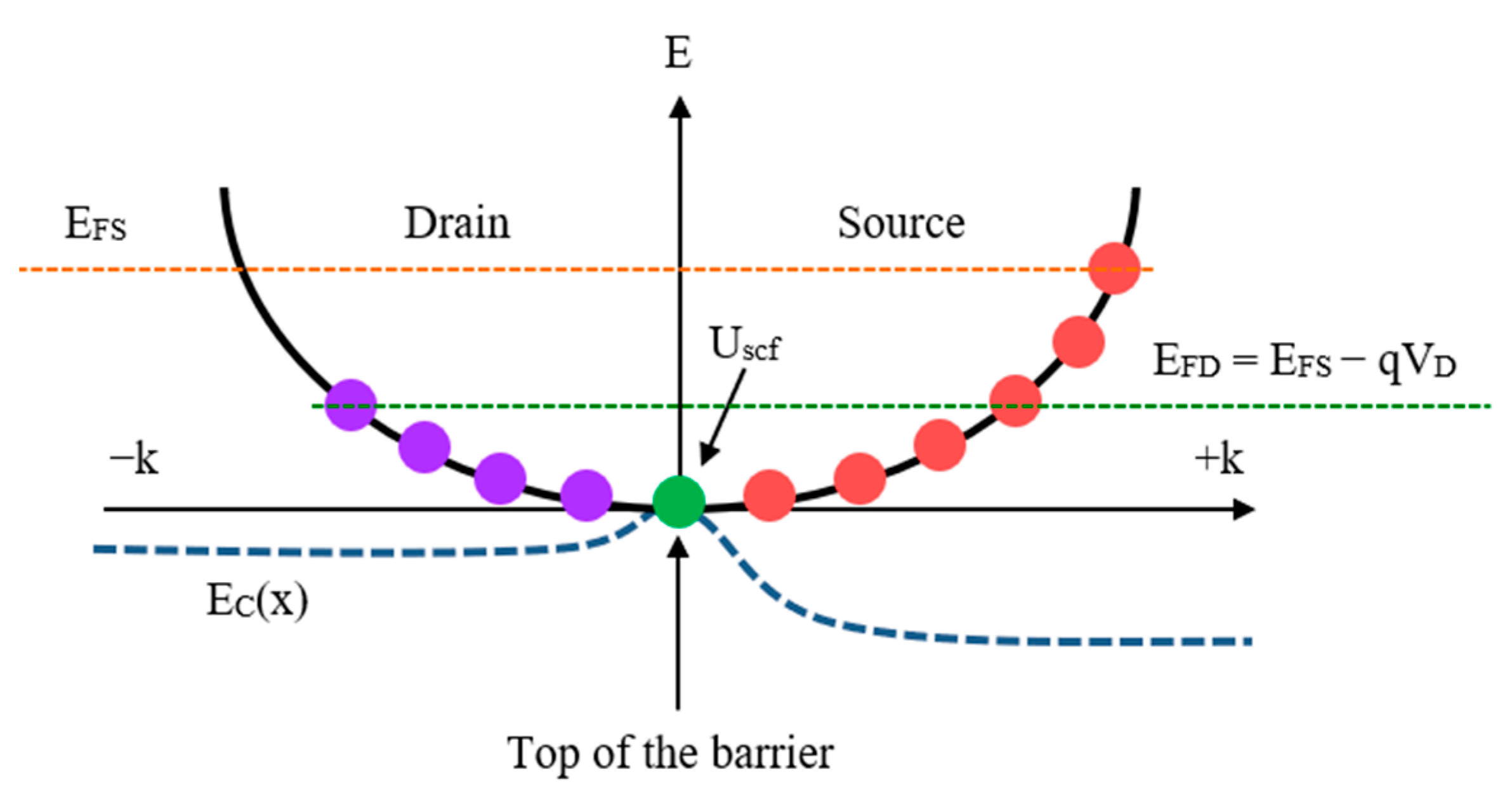
2. Device Modeling
2.1. Phonon Mean Free Path
2.2. Transmission Probability
3. Results and Discussion
4. Conclusions
Author Contributions
Funding
Data Availability Statement
Acknowledgments
Conflicts of Interest
Appendix A
References
- Wei, S.; Zhang, G.; Shao, Z.; Geng, L.; Yang, C.-F. Analysis of a high-performance ultra-thin body ultra-thin box silicon-on-insulator MOSFET with the lateral dual-gates: Featuring the suppression of the DIBL. Microsyst. Technol. 2018, 24, 3949–3956. [Google Scholar] [CrossRef] [Green Version]
- Zhang, S. Review of Modern Field Effect Transistor Technologies for Scaling. J. Phys. Conf. Ser. 2020, 1617, 012054. [Google Scholar] [CrossRef]
- Novoselov, K.S.; Geim, A.K.; Morozov, S.V.; Jiang, D.-e.; Zhang, Y.; Dubonos, S.V.; Grigorieva, I.V.; Firsov, A.A. Electric field effect in atomically thin carbon films. Science 2004, 306, 666–669. [Google Scholar] [CrossRef] [PubMed] [Green Version]
- Jing, S.; Wang, Y.; Chen, W.; Pan, J.; Li, W.; Bian, B.; Liao, B. Device Simulation of 5.1 nm High-Performance Field-Effect Transistors Based on Two-Dimensional Boron Phosphide. J. Phys. Chem. C 2022, 126, 12091–12099. [Google Scholar] [CrossRef]
- Wang, J.; Liu, W.; Wang, C. High-Performance Black Phosphorus Field-Effect Transistors with Controllable Channel Orientation. Adv. Electron. Mater. 2023, 9, 2201126. [Google Scholar] [CrossRef]
- Sang, P.; Wang, Q.; Wei, W.; Tai, L.; Zhan, X.; Li, Y.; Chen, J. Two-dimensional silicon atomic layer field-effect transistors: Electronic property, metal-semiconductor contact, and device performance. IEEE Trans. Electron Devices 2022, 69, 2173–2179. [Google Scholar] [CrossRef]
- Novoselov, K.; Jiang, D.; Schedin, F.; Booth, T.; Khotkevich, V.; Morozov, S.; Geim, A. Two-dimensional atomic crystals. Proc. Natl. Acad. Sci. USA 2005, 102, 10451–10453. [Google Scholar] [CrossRef] [Green Version]
- Hong, S.; Zagni, N.; Choo, S.; Liu, N.; Baek, S.; Bala, A.; Yoo, H.; Kang, B.H.; Kim, H.J.; Yun, H.J. Highly sensitive active pixel image sensor array driven by large-area bilayer MoS2 transistor circuitry. Nat. Commun. 2021, 12, 3559. [Google Scholar] [CrossRef] [PubMed]
- Karimipour, M.; Khazraei, S.; Kim, B.J.; Boschloo, G.; Johansson, E.M. Efficiency and Stability Enhancement of Perovskite Solar Cells Utilizing a Thiol Ligand and MoS2 (100) Nanosheet Surface Modification. ACS Appl. Energy Mater. 2021, 4, 14080–14092. [Google Scholar] [CrossRef]
- Ding, X.; Peng, F.; Zhou, J.; Gong, W.; Slaven, G.; Loh, K.P.; Lim, C.T.; Leong, D.T. Defect engineered bioactive transition metals dichalcogenides quantum dots. Nat. Commun. 2019, 10, 41. [Google Scholar] [CrossRef]
- Kumar, A.; Faella, E.; Durante, O.; Giubileo, F.; Pelella, A.; Viscardi, L.; Intonti, K.; Sleziona, S.; Schleberger, M.; Di Bartolomeo, A. Optoelectronic memory in 2D MoS2 field effect transistor. J. Phys. Chem. Solids 2023, 179, 111406. [Google Scholar] [CrossRef]
- Slobodeniuk, A.O.; Koutenský, P.; Bartoš, M.; Trojánek, F.; Malý, P.; Novotný, T.; Kozák, M. Ultrafast valley-selective coherent optical manipulation with excitons in WSe2 and MoS2 monolayers. NPJ 2d Mater. Appl. 2023, 7, 17. [Google Scholar] [CrossRef]
- Ahmed, Z.; Shi, Q.; Ma, Z.; Zhang, L.; Guo, H.; Chan, M. Analytical monolayer MoS2 MOSFET modeling verified by first principle simulations. IEEE Electron Device Lett. 2019, 41, 171–174. [Google Scholar] [CrossRef]
- Ma, S.; Wang, Y.; Chen, X.; Wu, T.; Wang, X.; Tang, H.; Yao, Y.; Yu, H.; Sheng, Y.; Ma, J. Analog Integrated Circuits Based on Wafer-Level Two-Dimensional MoS2 Materials with Physical and SPICE Model. IEEE Access 2020, 8, 197287–197299. [Google Scholar] [CrossRef]
- Nandan, K.; Yadav, C.; Rastogi, P.; Toral-Lopez, A.; Marin-Sanchez, A.; Marin, E.G.; Ruiz, F.G.; Bhowmick, S.; Chauhan, Y.S. Compact modeling of multi-layered MoS2 FETs including negative capacitance effect. IEEE J. Electron Devices Soc. 2020, 8, 1177–1183. [Google Scholar] [CrossRef]
- Khare, A.; Dwivedi, P. Design, simulation and optimization of multi-layered MoS2 based FET devices. Eng. Res. Express 2021, 3, 045046. [Google Scholar] [CrossRef]
- Singh, N.K.; Kumari, M.; Sahoo, M. A compact short-channel analytical drain current model of asymmetric dual-gate TMD FET in subthreshold region including fringing field effects. IEEE Access 2020, 8, 207982–207990. [Google Scholar] [CrossRef]
- Zeng, J.; Deng, W.; Zhou, C.; Peng, J.; Huang, J. A Compact Model of MoS2 Field-Effect Transistors from Drift-Diffusion to Ballistic Carrier Transport Regimes. IEEE J. Electron Devices Soc. 2020, 8, 285–290. [Google Scholar] [CrossRef]
- Gholinataj-Jelodar, E.; Aghanejad Ahmadchally, A.; Gooran-Shoorakchaly, A.; Gholipour, M. Semi-analytical SPICE-compatible ballistic I–V model for 5 nm channel MoS2 FETs. J. Comput. Electron. 2022, 21, 1108–1115. [Google Scholar] [CrossRef]
- Silvestri, L.; Palsgaard, M.; Rhyner, R.; Frey, M.; Wellendorff, J.; Smidstrup, S.; Gull, R.; El Sayed, K. Hierarchical modeling for TCAD simulation of short-channel 2D material-based FETs. Solid-State Electron. 2023, 200, 108533. [Google Scholar] [CrossRef]
- Li, H.; Li, Y.; Jiang, H.; Mao, L.; Ni, Y. Characteristic analysis of the MoS2/SiO2 interface field-effect transistor with varying MoS2 layers. J. Mater. Sci. Mater. Electron. 2023, 34, 427. [Google Scholar] [CrossRef]
- Tiwari, S.; Dolai, S.; Rahaman, H.; Gupta, P.S. Effect of temperature & phonon scattering on the drain current of a MOSFET using SL-MoS2 as its channel material. Superlattices Microstruct. 2017, 111, 912–921. [Google Scholar]
- Pilotto, A.; Khakbaz, P.; Palestri, P.; Esseni, D. Semi-classical transport in MoS2 and MoS2 transistors by a Monte Carlo approach. Solid-State Electron. 2022, 192, 108295. [Google Scholar] [CrossRef]
- Guo, F.; Liu, Z.; Zhu, M.; Zheng, Y. Electron–phonon scattering limited hole mobility at room temperature in a MoS2 monolayer: First-principles calculations. Phys. Chem. Chem. Phys. 2019, 21, 22879–22887. [Google Scholar] [CrossRef] [PubMed]
- Khair, K.A.; Ahmed, S.S. Strain-dependent polar optical phonon scattering and drive current optimization in nanoscale monolayer MoS2 FETs. Electron. Mater. Lett. 2020, 16, 299–309. [Google Scholar] [CrossRef]
- Chai, Y.; Su, S.; Yan, D.; Ozkan, M.; Lake, R.; Ozkan, C.S. Strain gated bilayer molybdenum disulfide field effect transistor with edge contacts. Sci. Rep. 2017, 7, 41593. [Google Scholar] [CrossRef] [Green Version]
- Pető, J.; Dobrik, G.; Kukucska, G.; Vancsó, P.; Koós, A.A.; Koltai, J.; Nemes-Incze, P.; Hwang, C.; Tapasztó, L. Moderate strain induced indirect bandgap and conduction electrons in MoS2 single layers. NPJ 2d Mater. Appl. 2019, 3, 39. [Google Scholar] [CrossRef] [Green Version]
- Chen, Y.; Deng, W.; Chen, X.; Wu, Y.; Shi, J.; Zheng, J.; Chu, F.; Liu, B.; An, B.; You, C. Carrier mobility tuning of MoS2 by strain engineering in CVD growth process. Nano Res. 2021, 14, 2314–2320. [Google Scholar] [CrossRef]
- Kaushal, P.; Chaudhary, T.; Khanna, G. Effect of Tensile Strain on Performance Parameters of Different Structures of MoS2 Monolayer. Silicon 2021, 14, 4935–4943. [Google Scholar] [CrossRef]
- Rahman, A.; Guo, J.; Datta, S.; Lundstrom, M.S. Theory of ballistic nanotransistors. IEEE Trans. Electron Devices 2003, 50, 1853–1864. [Google Scholar] [CrossRef] [Green Version]
- Pierret, R.F. Advanced Semiconductor Fundamentals, 2nd ed.; Prentice Hall: Hoboken, NJ, USA, 2003; Volume 6. [Google Scholar]
- Mohammad Tabatabaei, S.; Noei, M.; Khaliji, K.; Pourfath, M.; Fathipour, M. A first-principles study on the effect of biaxial strain on the ultimate performance of monolayer MoS2-based double gate field effect transistor. J. Appl. Phys. 2013, 113, 163708. [Google Scholar] [CrossRef]
- El Grour, T.; Pasadas, F.; Medina-Rull, A.; Najari, M.; Marin, E.G.; Toral-Lopez, A.; Ruiz, F.G.; Godoy, A.; Jiménez, D.; El Mir, L. Compact Modeling of pH-Sensitive FETs Based on 2-D Semiconductors. IEEE Trans. Electron Devices 2021, 68, 5916–5919. [Google Scholar] [CrossRef]
- Xu, Y.; Sheng Li, W.; Fan, D.; Shi, Y.; Qiu, H.; Wang, X. A compact model for transition metal dichalcogenide field effect transistors with effects of interface traps. In Proceedings of the 2021 5th IEEE Electron Devices Technology & Manufacturing Conference (EDTM), Chengdu, China, 8–11 April 2021; pp. 1–3. [Google Scholar]
- Kormányos, A.; Burkard, G.; Gmitra, M.; Fabian, J.; Zólyomi, V.; Drummond, N.D.; Fal’ko, V. k·p theory for two-dimensional transition metal dichalcogenide semiconductors. 2D Mater. 2015, 2, 022001. [Google Scholar] [CrossRef]
- Kadantsev, E.S.; Hawrylak, P. Electronic structure of a single MoS2 monolayer. Solid State Commun. 2012, 152, 909–913. [Google Scholar] [CrossRef]
- Chuan, M.W.; Riyadi, M.A.; Hamzah, A.; Alias, N.E.; Sultan, S.M.; Lim, C.S.; Tan, M.L.P. Impact of phonon scattering mechanisms on the performance of silicene nanoribbon field-effect transistors. Results Phys. 2021, 29, 104714. [Google Scholar] [CrossRef]
- Murnal, V.R.; Vijaya, C. A quasi-ballistic drain current, charge and capacitance model with positional carrier scattering dependency valid for symmetric DG MOSFETs in nanoscale regime. Nano Converg. 2019, 6, 19. [Google Scholar] [CrossRef]
- Ahmed, S.N. Physics and Engineering of Radiation Detection; Elsevier Science: Amsterdam, The Netherlands, 2018. [Google Scholar]
- Cheng, L.; Zhang, C.; Liu, Y. Why two-dimensional semiconductors generally have low electron mobility. Phys. Rev. Lett. 2020, 125, 177701. [Google Scholar] [CrossRef]
- Shree, S.; Semina, M.; Robert, C.; Han, B.; Amand, T.; Balocchi, A.; Manca, M.; Courtade, E.; Marie, X.; Taniguchi, T. Observation of exciton-phonon coupling in MoSe2 monolayers. Phys. Rev. B 2018, 98, 035302. [Google Scholar] [CrossRef] [Green Version]
- Nakamura, K. Coherent Control of Optical Phonons in Solids. In Encyclopedia of Interfacial Chemistry; Elsevier: Amsterdam, The Netherlands, 2018; pp. 334–337. [Google Scholar]
- Shinozuka, Y. Electron–Lattice Interactions in Semiconductors; Jenny Stanford Publishing: Singapore, 2021. [Google Scholar]
- Ahmed, S.; Alam, K. Effects of phonon scattering on the performance of silicon nanowire transistors. In Proceedings of the International Conference on Electrical & Computer Engineering (ICECE 2010), Dhaka, Bangladesh, 18–20 December 2010; pp. 226–229. [Google Scholar]
- Cai, Y.; Lan, J.; Zhang, G.; Zhang, Y.-W. Lattice vibrational modes and phonon thermal conductivity of monolayer MoS2. Phys. Rev. B 2014, 89, 035438. [Google Scholar] [CrossRef] [Green Version]
- Chandrasekar, H.; Ganapathi, K.L.; Bhattacharjee, S.; Bhat, N.; Nath, D.N. Optical-Phonon-Limited High-Field Transport in Layered Materials. IEEE Trans. Electron Devices 2015, 63, 767–772. [Google Scholar] [CrossRef] [Green Version]
- Laturia, A.; Van de Put, M.L.; Vandenberghe, W.G. Dielectric properties of hexagonal boron nitride and transition metal dichalcogenides: From monolayer to bulk. npj 2D Mater. Appl. 2018, 2, 6. [Google Scholar] [CrossRef] [Green Version]
- Chatterjee, A.K.; Kushwaha, M.; Prasad, B. Analytical Model for Drain Current of a Ballistic MOSFET. Silicon 2021, 13, 1777–1785. [Google Scholar] [CrossRef]
- Lundstrom, M.S. Fundamentals of Nanotransistors; World Scientific Publishing Company: Hackensack, NJ, USA; London, UK, 2017; Volume 6. [Google Scholar]
- Kumar, J.; Sheoran, G.; Shrivastava, M. Electrothermal transport induced material reconfiguration and performance degradation of CVD-grown monolayer MoS2 transistors. npj 2D Mater. Appl. 2020, 4, 37. [Google Scholar]
- Khan, M.A.U.; Srivastava, A.; Mayberry, C.; Sharma, A.K. Analytical current transport modeling of monolayer molybdenum disulfide-based dual gate tunnel field effect transistor. IEEE Trans. Nanotechnol. 2020, 19, 620–627. [Google Scholar] [CrossRef]
- Khan, M.; Tripathi, M.N.; Tripathi, A. Strain-induced structural, elastic, and electronic properties of 1L-MoS2. J. Mater. Res. 2022, 37, 3340–3351. [Google Scholar] [CrossRef]
- Hosseini, M.; Elahi, M.; Pourfath, M.; Esseni, D. Strain-Induced Modulation of Electron Mobility in Single-Layer Transition Metal Dichalcogenides MX2 ( M = Mo, W.; X = S, Se). IEEE Trans. Electron Devices 2015, 62, 3192–3198. [Google Scholar] [CrossRef]
- Chong, C.; Liu, H.; Wang, S.; Yang, K. First-principles study on the effect of strain on single-layer molybdenum disulfide. Nanomaterials 2021, 11, 3127. [Google Scholar] [CrossRef]
- Piacentini, A.; Marian, D.; Schneider, D.S.; González Marín, E.; Wang, Z.; Otto, M.; Canto, B.; Radenovic, A.; Kis, A.; Fiori, G. Stable Al2O3 Encapsulation of MoS2-FETs Enabled by CVD Grown h-BN. Adv. Electron. Mater. 2022, 8, 2200123. [Google Scholar] [CrossRef]
- Kawanago, T.; Oba, T.; Oda, S. Transfer printing of Al2O3 gate dielectric for fabrication of top-gate MoS2 FET. Appl. Phys. Express 2019, 12, 026501. [Google Scholar] [CrossRef]
- Ryu, J.H.; You, Y.G.; Kim, S.W.; Hong, J.H.; Na, J.H.; Jhang, S.H. Effect of Al2O3 deposition on carrier mobility and ambient stability of few-layer MoS2 field effect transistors. Curr. Appl. Phys. 2020, 20, 363–365. [Google Scholar] [CrossRef]
- Song, X.; Xu, J.; Liu, L.; Deng, Y.; Lai, P.-T.; Tang, W.-M. Optimizing Al-doped ZrO2 as the gate dielectric for MoS2 field-effect transistors. Nanotechnology 2020, 31, 135206. [Google Scholar] [CrossRef] [PubMed]
- Kol, S.; Oral, A. Hf-Based High-κ Dielectrics: A Review. Acta Phys. Pol. A 2019, 136, 873–881. [Google Scholar] [CrossRef]
- Divya, N.B.; Sivasankaran, K. Impact of MgO interfacial layer of gate dielectric engineered monolayer MoS2 FET. In Computer-Aided Developments: Electronics and Communication; CRC Press: Boca Raton, FL, USA, 2019; pp. 239–245. [Google Scholar]
- Song, X.-J.; Xu, L.-C.; Bai, H.-F.; Li, Y.; Ma, Z.; Yang, Z.; Liu, R.; Li, X. Effects of high-k dielectric environment on the full ballistic transport properties of monolayer MoS2 FETs. J. Appl. Phys. 2017, 121, 144505. [Google Scholar] [CrossRef]
- Bha, J.K.; Priya, P.A.; Joseph, H.B.; Thiruvadigal, D.J. 10 nm Trigate high k underlap finFETs: Scaling effects and analog performance. Silicon 2020, 12, 2111–2119. [Google Scholar] [CrossRef]
- Kumar, S.A.; Pravin, J.C. Analysis of Multi Bridge Channel Undoped Trigate MOSFET by Different High-k Dielectrics for Sub 10 nm. Silicon 2022, 14, 5535–5543. [Google Scholar] [CrossRef]
- Kosmani, N.F.; Hamid, F.A.; Razali, M.A. Effects of high-k dielectric materials on electrical performance of double gate and gate-all-around mosfet. Int. J. Integr. Eng. 2020, 12, 81–88. [Google Scholar]
- Zhao, X.-Y.; Xu, J.-P.; Liu, L.; Li, Z. Improved Electrical Properties of Top-Gate MoS2 Transistor with NH3-Plasma Treated HfO2 as Gate Dielectric. IEEE Electron Device Lett. 2020, 41, 1364–1367. [Google Scholar] [CrossRef]
- Sun, X.; Zhang, Y.; Jia, K.; Tian, G.; Yu, J.; Xiang, J.; Yang, R.; Wu, Z.; Yin, H. Improved performance of MoS2 FET by in situ NH3 doping in ALD Al2O3 dielectric. Chin. Phys. B 2022, 31, 077701. [Google Scholar] [CrossRef]
- Pan, Y.; Jia, K.; Huang, K.; Wu, Z.; Bai, G.; Yu, J.; Zhang, Z.; Zhang, Q.; Yin, H. Near-ideal subthreshold swing MoS2 back-gate transistors with an optimized ultrathin HfO2 dielectric layer. Nanotechnology 2019, 30, 095202. [Google Scholar] [CrossRef] [PubMed]
- Kumar, S.; Sharma, A.; Tomar, M.; Gupta, V. Realization of low-power and high mobility thin film transistors based on MoS2 layers grown by PLD technique. Mater. Sci. Eng. B 2021, 266, 115047. [Google Scholar] [CrossRef]
- Xie, J.; Patoary, N.M.; Zhou, G.; Sayyad, M.Y.; Tongay, S.; Esqueda, I.S. Analysis of Schottky barrier heights and reduced Fermi-level pinning in monolayer CVD-grown MoS2 field-effect-transistors. Nanotechnology 2022, 33, 225702. [Google Scholar] [CrossRef] [PubMed]


| Dual-Gate Device | Single-Gate Device | Single-Gate Device | ||||
|---|---|---|---|---|---|---|
| Parameters | Our Study | Other Model [19] | Our Study | Experimental Data [67] | Our Study | Experimental Data [68] |
| Channel length, L | 5 nm | 5 nm | 16 µm | 16 µm | 20 µm | 20 µm |
| Temperature, T (K) | 300 | 300 | 300 | 300 | 300 | 300 |
| Dielectric constant, k | 16 | 16 | 25 | 25 | 3.9 | 3.9 |
| Oxide thickness, Tox (nm) | 2 | 2 | 10 | 10 | 90 | 90 |
| SS (mV/dec) | 153.5 | 157.0 | 76.4 | 77.6 | 359 | 360 |
| On–off ratio | 103 | 103 | 104 | 104 | 105 | 105 |
Disclaimer/Publisher’s Note: The statements, opinions and data contained in all publications are solely those of the individual author(s) and contributor(s) and not of MDPI and/or the editor(s). MDPI and/or the editor(s) disclaim responsibility for any injury to people or property resulting from any ideas, methods, instructions or products referred to in the content. |
© 2023 by the authors. Licensee MDPI, Basel, Switzerland. This article is an open access article distributed under the terms and conditions of the Creative Commons Attribution (CC BY) license (https://creativecommons.org/licenses/by/4.0/).
Share and Cite
Chin, H.C.; Hamzah, A.; Alias, N.E.; Tan, M.L.P. Modeling the Impact of Phonon Scattering with Strain Effects on the Electrical Properties of MoS2 Field-Effect Transistors. Micromachines 2023, 14, 1235. https://doi.org/10.3390/mi14061235
Chin HC, Hamzah A, Alias NE, Tan MLP. Modeling the Impact of Phonon Scattering with Strain Effects on the Electrical Properties of MoS2 Field-Effect Transistors. Micromachines. 2023; 14(6):1235. https://doi.org/10.3390/mi14061235
Chicago/Turabian StyleChin, Huei Chaeng, Afiq Hamzah, Nurul Ezaila Alias, and Michael Loong Peng Tan. 2023. "Modeling the Impact of Phonon Scattering with Strain Effects on the Electrical Properties of MoS2 Field-Effect Transistors" Micromachines 14, no. 6: 1235. https://doi.org/10.3390/mi14061235