
Multipoint Lock-in Detection for Diamond Nitrogen-Vacancy Magnetometry Using DDS-Based Frequency-Shift Keying


Abstract
:1. Introduction
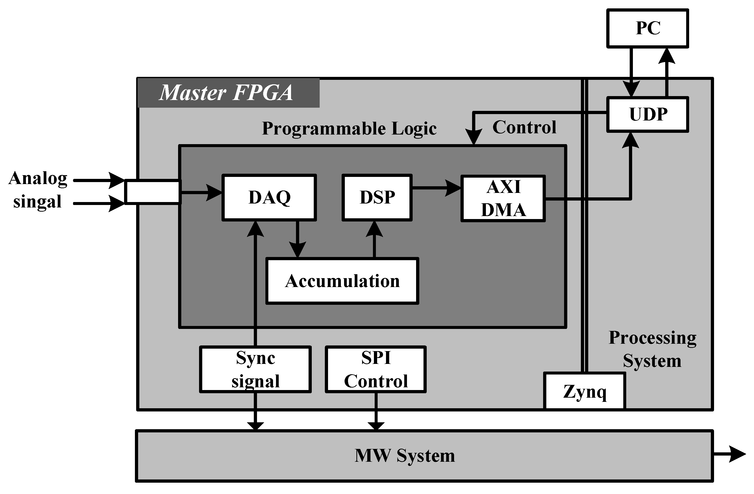
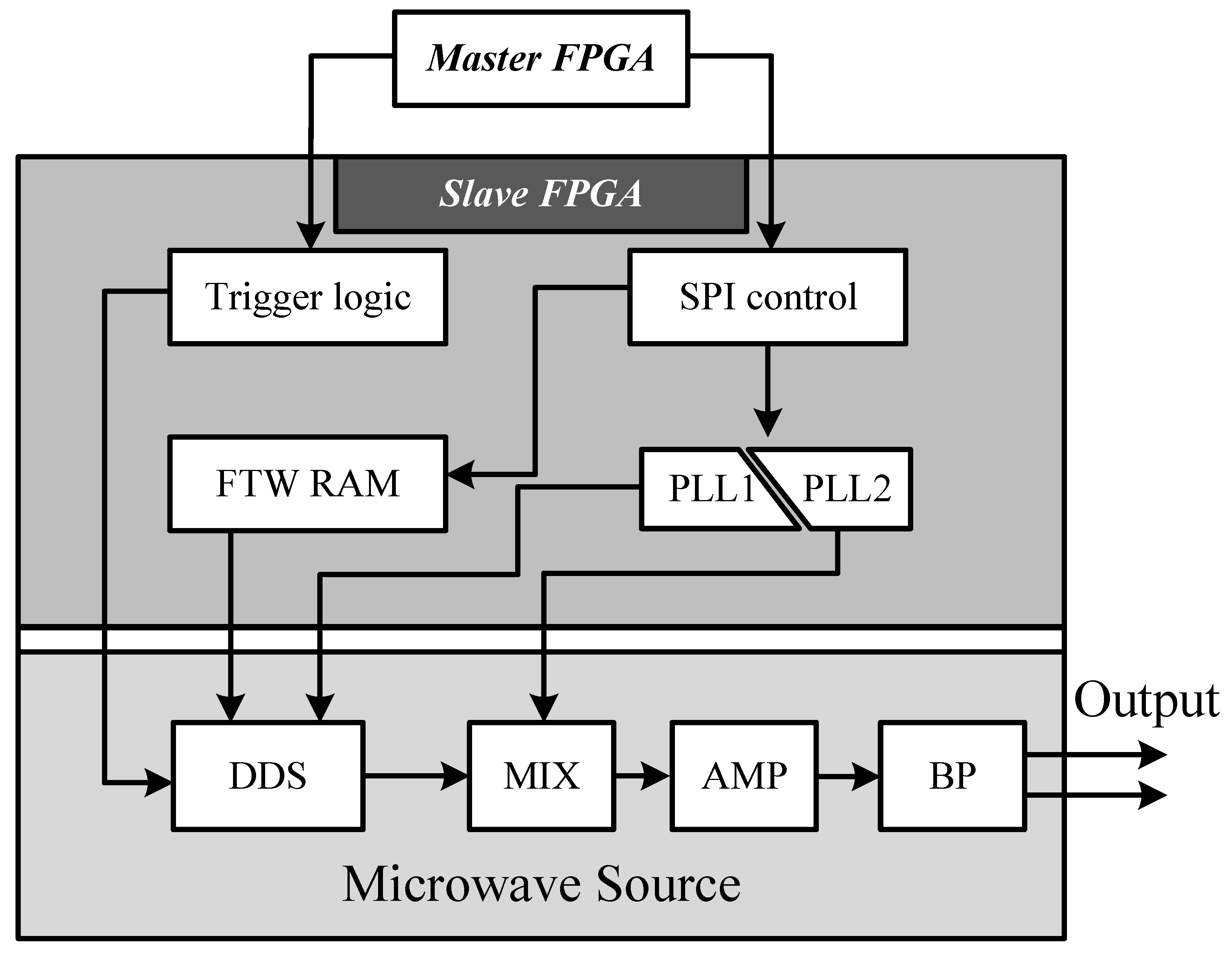
2. Implementation
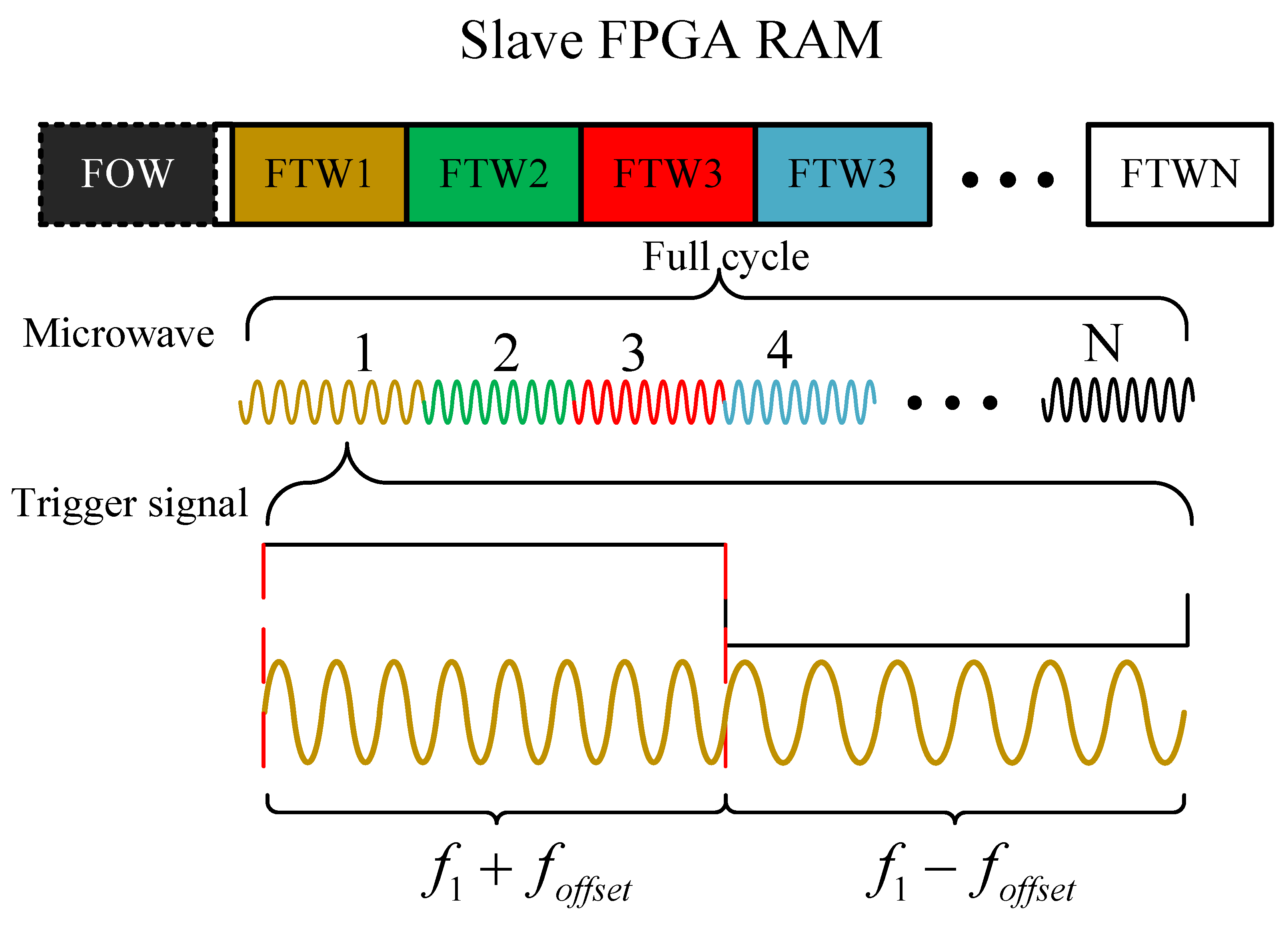
2.1. Microwave Source
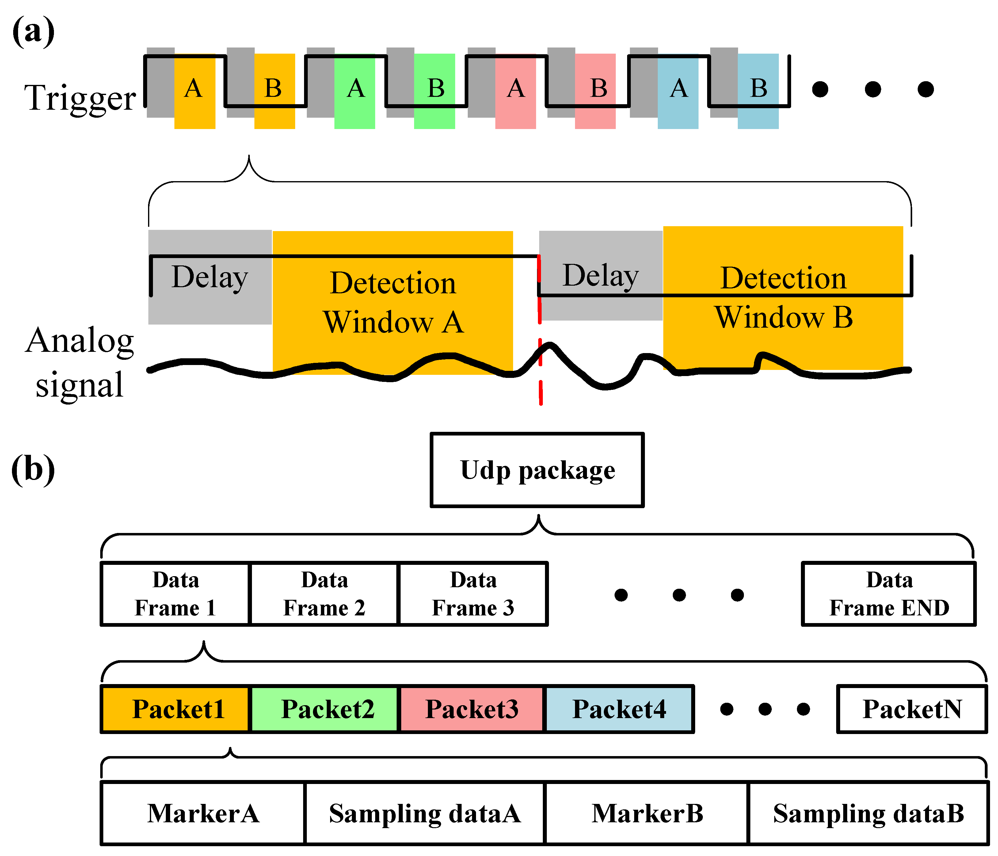
2.2. Signal Sampling and Processing
2.3. Experiment Setup
3. Result
3.1. General-Purpose Experiment of NV Ensembles
3.2. Multipoint Lock-in Detection
4. Conclusions
Author Contributions
Funding
Data Availability Statement
Conflicts of Interest
References
- Barry, J.F.; Schloss, J.M.; Bauch, E.; Turner, M.J.; Hart, C.A.; Pham, L.M.; Walsworth, R.L. Sensitivity optimization for nv-diamond magnetometry. Rev. Mod. Phys. 2020, 92, 015004. [Google Scholar] [CrossRef]
- Zhang, J.; Hegde, S.S.; Suter, D. Efficient implementation of a quantum algorithm in a single nitrogen-vacancy center of diamond. Phys. Rev. Lett. 2020, 125, 030501. [Google Scholar] [CrossRef] [PubMed]
- Neumann, P.; Mizuochi, N.; Rempp, F.; Hemmer, P.; Watanabe, H.; Yamasaki, S.; Gaebel, T.; Jelezko, F.; Wrachtrup, J. Multipartite entanglement among single spins in diamond. Science 2008, 320, 1326–1329. [Google Scholar] [CrossRef] [PubMed]
- Shi, F.; Zhang, Q.; Naydenov, B.; Jelezko, F.; Du, J.; Reinhard, F.; Wrachtrup, J. Quantum logic readout and cooling of a single dark electron spin. Phys. Rev. B 2013, 87, 195414. [Google Scholar] [CrossRef]
- Kong, F.; Ju, C.; Liu, Y.; Lei, C.; Wang, M.; Kong, X.; Wang, P.; Huang, P.; Li, Z.; Shi, F.; et al. Direct measurement of topological numbers with spins in diamond. Phys. Rev. Lett. 2016, 117, 060503. [Google Scholar] [CrossRef] [PubMed]
- Wang, Y.; Dolde, F.; Biamonte, J.; Babbush, R.; Bergholm, V.; Yang, S.; Jakobi, I.; Aspuru-Guzik, A.; Whitfield, J.D.; Whitfield, J.D.; et al. Quantum simulation of helium hydride cation in a solid-state spin register. ACS Nano 2015, 9, 7769–7774. [Google Scholar] [CrossRef]
- Maze, J.R.; Stanwix, P.L.; Hodges, J.S.; Hong, S.; Taylor, J.M.; Cappellaro, P.; Dutt, M.V.G.; Togan, E.; Zibrov, A.S.; Yacoby, A.; et al. Nanoscale magnetic sensing with an individual electronic spin in diamond. Nature 2008, 455, 644–647. [Google Scholar] [CrossRef]
- Hall, L.T.; Beart, G.C.G.; Thomas, E.A.; Simpson, D.A.; McGuinness, L.P.; Manton, J.H.; Scholten, R.E.; Jelezko, F.; Wrachtrup, J.; Hollenberg, L.C.L. High spatial and temporal resolution wide-field imaging of neuron activity using quantum nv-diamond. Sci. Rep. 2012, 2, 401. [Google Scholar] [CrossRef]
- Jakobi, I.; Neumann, P.; Wang, Y.; Dasari, D.B.R.; El Hallak, F.; Bashir, M.A.; Edmonds, A.; Twitchen, D.; Wrachtrup, J. Measuring broadband magnetic fields on the nanoscale using a hybrid quantum register. Nat. Nanotechnol. 2017, 12, 67–72. [Google Scholar] [CrossRef]
- Shim, J.H.; Lee, S.-J.; Ghimire, S.; Hwang, J.I.; Lee, K.-G.; Kim, K.; Turner, M.J.; Hart, C.A.; Walsworth, R.L.; Oh, S. Multiplexed sensing of magnetic field and temperature in real time using a nitrogen-vacancy ensemble in diamond. Phys. Rev. Appl. 2022, 17, 014009. [Google Scholar] [CrossRef]
- Schoenfeld, R.S.; Harneit, W. Real time magnetic field sensing and imaging using a single spin in diamond. Phys. Rev. Lett. 2011, 106, 030802. [Google Scholar] [CrossRef] [PubMed]
- Dolde, F.; Fedder, H.; Doherty, M.W.; Nöbauer, T.; Rempp, F.; Wolf, T.; Reinhard, F.; Hollenberg, L.C.L.; Jelezko, F. Electric-field sensing using single diamond spins. Nat. Phys. 2011, 7, 459–463. [Google Scholar] [CrossRef]
- Li, R.; Kong, F.; Zhao, P.; Cheng, Z.; Qin, Z.; Wang, M.; Zhang, Q.; Wang, P.; Wang, Y.; Du, J. Nanoscale electrometry based on a magnetic-field-resistant spin sensor. Phys. Rev. Lett. 2020, 124, 247701. [Google Scholar] [CrossRef] [PubMed]
- Kucsko, G.; Maurer, P.C.; Yao, N.Y.; Kubo, M.; Noh, H.J.; Lo, P.K.; Park, H.; Lukin, M.D. Nanometre-scale thermometry in a living cell. Nature 2013, 500, 54–58. [Google Scholar] [CrossRef] [PubMed]
- Neumann, P.; Jakobi, I.; Dolde, F.; Burk, C.; Reuter, R.; Waldherr, G.; Honert, J.; Wolf, T.; Brunner, A.; Shim, J.H.; et al. High-precision nanoscale temperature sensing using single defects in diamond. Nano Lett. 2013, 13, 2738–2742. [Google Scholar] [CrossRef] [PubMed]
- Doherty, M.W.; Struzhkin, V.V.; Simpson, D.A.; McGuinness, L.P.; Meng, Y.; Karle, T.J.; Hemley, R.J.; Manson, N.B.; Hollenberg, L.C.; Hollenberg, L.C.L.; et al. Electronic properties and metrology applications of the diamond nv- center under pressure. Phys. Rev. Lett. 2014, 112, 047601. [Google Scholar] [CrossRef] [PubMed]
- Barry, J.F.; Turner, M.J.; Schloss, J.M.; Glenn, D.R.; Song, Y.; Lukin, M.D.; Walsworth, R.L. Optical magnetic detection of single-neuron action potentials using quantum defects in diamond. Proc. Natl. Acad. Sci. USA 2016, 113, 14133–14138. [Google Scholar] [CrossRef] [PubMed]
- Stimpson, G.; Skilbeck, M.; Patel, R.; Green, B.L.; Morley, G. An open-source high-frequency lock-in amplifier. Rev. Sci. Instrum. 2019, 90, 094701. [Google Scholar] [CrossRef]
- Schloss, J.M.; Barry, J.F.; Turner, M.J.; Walsworth, R.L. Simultaneous broadband vector magnetometry using solid-state spins. Phys. Rev. Appl. 2018, 10, 034044. [Google Scholar] [CrossRef]
- Santarini, M. Xilinx redefines state of the art with new 7 series fpgas. Xcell J. 2010, 3, 6–11. [Google Scholar]
- Tierney, J.; Rader, C.; Gold, B. A digital frequency synthesizer. IEEE Trans. Audio Electroacoust. 1971, 19, 48–57. [Google Scholar] [CrossRef]
- Arablu, M.; Kafashi, S.; Smith, S.T. Synchronous radio-frequency fm signal generator using direct digital synthesizers. Rev. Sci. Instrum. 2018, 89, 045009. [Google Scholar] [CrossRef] [PubMed]
- Qin, X.; Shi, Z.; Xie, Y.; Wang, L.; Rong, X.; Jia, W.; Zhang, W.; Du, J. An integrated device with high performance multi-function generators and time-to-digital convertors. Rev. Sci. Instrum. 2017, 88, 014702. [Google Scholar] [CrossRef] [PubMed]
- Przybus, B. Xilinx Redefines Power, Performance, and Design Productivity with Three New 28 nm Fpga Families: Virtex-7, Kintex-7, and Artix-7 Devices. Xilinx White Paper. 2010. Available online: http://xilinx.eepw.com.cn/share/show/s/285 (accessed on 16 October 2023).
- Vindhya, K.; Bharathi, B.; Shenoy, N.R.; Kamala, C. Performance evaluation of wide bandwidth rf signal generator chip. Int. J. Adv. Eng. Res. Sci. 2017, 4, 237264. [Google Scholar]
- Anand, N.; Joseph, G.; Oommen, S.S.; Dhanabal, R. Design and implementation of a high speed serial peripheral interface. In Proceedings of the 2014 International Conference on Advances in Electrical Engineering (ICAEE), Vellore, India, 9–11 January 2014; IEEE: Piscataway, NJ, USA, 2014; pp. 1–3. [Google Scholar]
- Liu, Y.; Ye, R.; Hu, Q.; Chen, B.; Zhang, W.; Zhou, F.; Xu, N. A dds-based integrated microwave source for fast frequency sweeping in quantum magnetic-resonance systems. AIP Adv. 2023, 13, 015009. [Google Scholar] [CrossRef]
- Steiner, M.; Neumann, P.; Beck, J.; Jelezko, F.; Wrachtrup, J. Universal enhancement of the optical readout fidelity of single electron spins at nitrogen-vacancy centers in diamond. Phys. Rev. B 2010, 81, 035205. [Google Scholar] [CrossRef]
- Tetienne, J.; Rondin, L.; Spinicelli, P.; Chipaux, M.; Debuisschert, T.; Roch, J.; Jacques, V. Magnetic-field-dependent photodynamics of single nv defects in diamond: An application to qualitative all-optical magnetic imaging. New J. Phys. 2012, 14, 103033. [Google Scholar] [CrossRef]
- Wang, N.; Liu, C.-F.; Fan, J.-W.; Feng, X.; Leong, W.-H.; Finkler, A.; Denisenko, A.; Li, Q.; Liu, R.-B. Zero-field magnetometry using hyperfine-biased nitrogen-vacancy centers near diamond surfaces. Phys. Rev. Res. 2022, 4, 013098. [Google Scholar] [CrossRef]
- Kitazawa, S.; Matsuzaki, Y.; Saijo, S.; Kakuyanagi, K.; Saito, S.; Ishi-Hayase, J. Vector-magnetic-field sensing via multifrequency control of nitrogen-vacancy centers in diamond. Phys. Rev. A 2017, 96, 042115. [Google Scholar] [CrossRef]
- Ambal, K.; McMichael, R.D. A differential rate meter for real-time peak tracking in optically detected magnetic resonance at low photon count rates. Rev. Sci. Instrum. 2019, 90, 023907. [Google Scholar] [CrossRef]


Disclaimer/Publisher’s Note: The statements, opinions and data contained in all publications are solely those of the individual author(s) and contributor(s) and not of MDPI and/or the editor(s). MDPI and/or the editor(s) disclaim responsibility for any injury to people or property resulting from any ideas, methods, instructions or products referred to in the content. |
© 2023 by the authors. Licensee MDPI, Basel, Switzerland. This article is an open access article distributed under the terms and conditions of the Creative Commons Attribution (CC BY) license (https://creativecommons.org/licenses/by/4.0/).
Share and Cite
Hu, Q.; Cheng, L.; Liu, Y.; Zhu, X.; Tian, Y.; Xu, N. Multipoint Lock-in Detection for Diamond Nitrogen-Vacancy Magnetometry Using DDS-Based Frequency-Shift Keying. Micromachines 2024, 15, 14. https://doi.org/10.3390/mi15010014
Hu Q, Cheng L, Liu Y, Zhu X, Tian Y, Xu N. Multipoint Lock-in Detection for Diamond Nitrogen-Vacancy Magnetometry Using DDS-Based Frequency-Shift Keying. Micromachines. 2024; 15(1):14. https://doi.org/10.3390/mi15010014
Chicago/Turabian StyleHu, Qidi, Luheng Cheng, Yushan Liu, Xinyi Zhu, Yu Tian, and Nanyang Xu. 2024. "Multipoint Lock-in Detection for Diamond Nitrogen-Vacancy Magnetometry Using DDS-Based Frequency-Shift Keying" Micromachines 15, no. 1: 14. https://doi.org/10.3390/mi15010014