Article

A Novel 6500 V SiC Trench MOSFET with Integrated Unipolar Diode for Improved Third Quadrant and Switching Characteristics

1
State Key Laboratory of Electronic Thin Films and Integrated Devices, University of Electronic Science and Technology of China, Chengdu 610054, China
2
Shenzhen Institute for Advanced Study, University of Electronic Science and Technology of China, Shenzhen 518110, China
*
Author to whom correspondence should be addressed.
Micromachines 2024, 15(1), 92; https://doi.org/10.3390/mi15010092
Submission received: 28 April 2023 / Revised: 22 December 2023 / Accepted: 25 December 2023 / Published: 31 December 2023
(This article belongs to the Section D1: Semiconductor Devices)

Abstract

:
A 6500 V SiC trench MOSFET with integrated unipolar diode (UD-MOS) is proposed to improve reverse conduction characteristics, suppress bipolar degradation, and reduce switching loss. An N type base region under the trench dummy gate provides a low barrier path to suppress hole injection during the reverse conduction operation. The reverse conduction voltage VON is reduced to 1.11 V, and the reverse recovery charge (QRR) is reduced to 1.22 μC/cm2. The gate-to-drain capacitance (CGD) and gate-to-source capacitance (CGS) of the UD-MOS are also reduced to improve switching loss due to the thick oxide layer between the trench gate and dummy gate. The proposed device exhibits an excellent loss-related figure of merit (FOM). It provides a high-voltage SiC MOSFET prototype with potential performance advantages for voltage source converter-based high voltage direct current applications.

1. Introduction

The voltage source converter-based high-voltage direct current (VSC-HVDC) transmission with high flexibility and controllability is a key approach to the construction of a high-proportion clean energy grid. The high-voltage (6500 V and above) SiC MOSFET is a promising candidate for VSC-HVDC transmission to increase power efficiency and reduce the volume of the system [1,2,3]. In the VSC, the freewheeling diode of SiC MOSFET operates during the dead time period. However, the utilization of the integrated PN body diode causes potential issues. Firstly, the reverse recovery charge QRR and reverse conduction voltage VON considerably increase loss. Secondly, the basic plane dislocations (BPDs) generate stacking faults (SFs) in the drift region by absorbing the energy from charge recombination [4], which degrades the VON and leakage current of SiC MOSFET [5]. For the 6500 V SiC MOSFET with a thicker drift region, many more SFs could be generated based on same initial BPDs density, spelling more serious bipolar degradation issues [6].
To prevent SiC MOSFET bipolar degradation issues, a common solution is utilizing the externally antiparallel Schottky barrier diode (SBD) for freewheeling operation [7], but this increases the parasitic parameters and size of the MOSFETs-based power module [8]. However, for the monolithic integrated diode schemes, SBD-integrated MOSFETs have been reported [9,10,11] and the source-controlled channel-diode-embedded SiC MOSFETs have been demonstrated [12,13], whereas Schottky contact and the uneven gate oxide layer-related reliability issues have yet to be introduced [14,15,16,17]. Gate-controlled channel-diode-embedded SiC MOSFETs have also been fabricated [18,19,20], which allow the forward and reverse conduction currents to share the same MOS-channel path. However, this brings a huge challenge to achieving a better trade-off between low reverse conduction voltage and reasonable threshold voltage [18].
In this paper, a 6500 V SiC trench MOSFET with integrated unipolar diode (UD-MOS) is proposed to improve reverse conduction characteristics, suppress bipolar degradation issue, and reduce switching loss. Compared with the asymmetric trench MOSFET (C-MOS), the performance with its operation mechanism of UD-MOS is demonstrated by numerical simulations, involving doping-dependent mobility, high-field saturation mobility, Shockley–Read–Hall (SRH) recombination, Auger recombination, incomplete ionization of impurities, and impact ionization models.

2. Device Structure and Mechanism

The schematic cross-section view of the 6500 V SiC C-MOS and UD-MOS is shown in Figure 1. Compared with the C-MOS, the polysilicon gate of UD-MOS splits into two parts with a thick oxide layer. The left one is the true gate electrically connected to the gate electrode, while the right one is the dummy gate electrically connected to the source electrode. An N type region (i.e., N base region) beneath the dummy gate for electrons from the CSL region to N+ region, forms a unipolar diode (UD) as illustrated in Figure 1b.
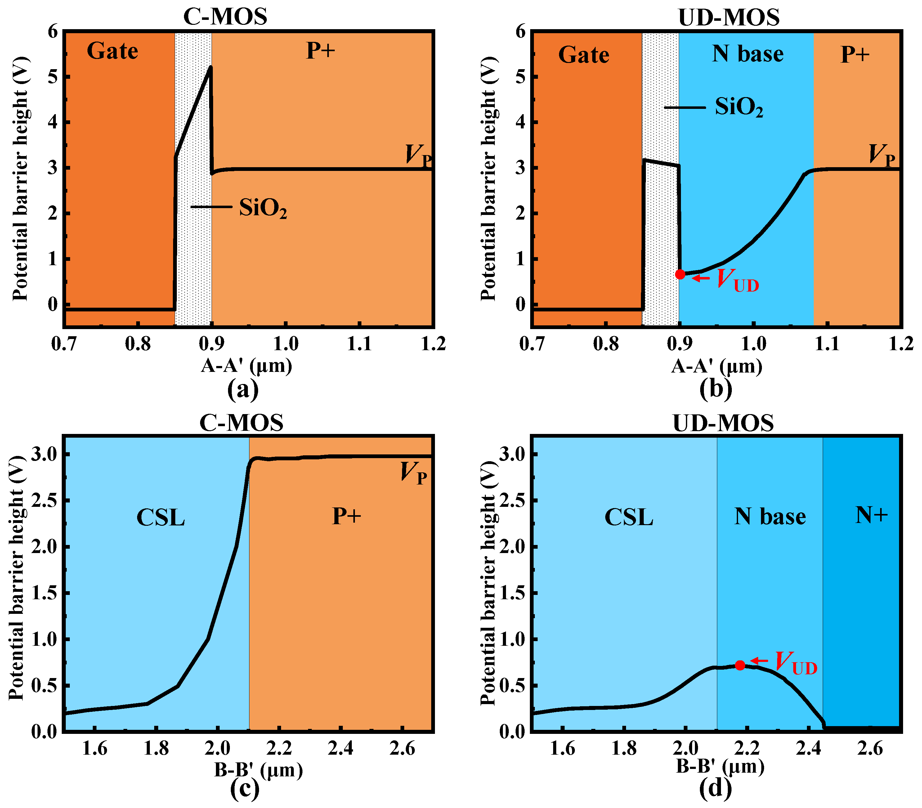
For the zero-bias condition, the potential barrier distribution of the integrated unipolar diode of UD-MOS is shown in Figure 2. Compared with the body diode of C-MOS, the decrease of potential barrier from the P+ region to the SiC/SiO2 interface (i.e., along line A′-A of Figure 1) makes a relatively low potential barrier (i.e., VUD) for electrons transported from the CSL to N+ region. It should be noted that the VUD is still relatively higher than the potential barrier of the CSL region and the N+ region as shown in Figure 2d. In other words, the electrons cannot flow through the N base region to the N+ region under this condition.
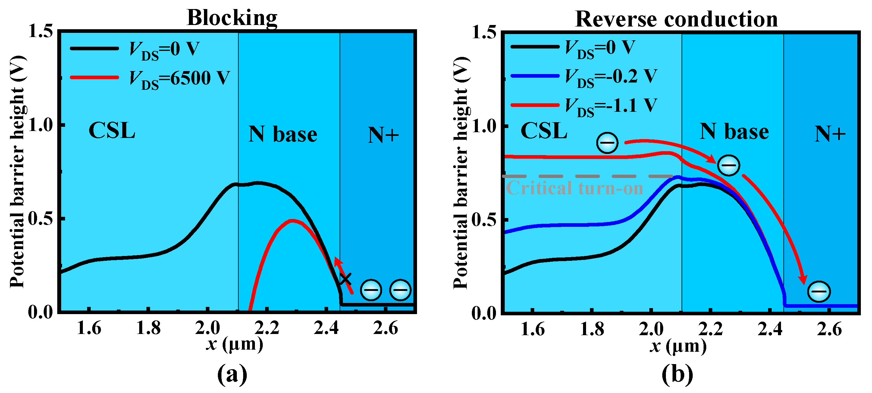
When in blocking condition, although the increasing VDS lowers the barrier of the CSL region and N base region due to the drain-induced barrier lowering effect, the VUD is still high enough to ensure blocking capability, as shown in Figure 3a. When in the reverse conduction condition, the potential barrier of the CSL region is raised by the negative VDS. Once the potential barrier of the CSL region exceeds VUD, the electrons from the CSL region can flow through the N base region to the N+ region, as shown in Figure 3b. Therefore, the potential height of the N base region determines both the blocking and reverse conduction characteristics of UD-MOS. Furthermore, a barrier height analysis model is given here to inform the design of the VUD as follows,
V UD = V P ϕ Si , SiC + V GS q N CH t CH 2 2 ε SiC ε SiC t ox ε ox t nch + 1 q N CH t CH 2 2 ε SiC
where VP is the potential barrier height of P+ region, ϕSi,SiC is the work function difference between N-type polysilicon and the P+ region, εSiC is the dielectric constant of SiC, εox is the dielectric constant of oxide, q is the elementary charge, tCH is the thickness of the N base region, and NCH is the doping concentration of the N base region, respectively. According to (1), even though the negative VGS can enhance blocking capability by increasing the VUD, it also results in a high reverse conduction voltage VON of UD-MOS. Moreover, the positive VGS even reduces the VUD to make the unipolar diode turn on, causing the UD-MOS to lose gate control when in the forward conduction condition [17]. Therefore, the dummy gate not controlled by the gate electrode is introduced to guarantee both the forward and reverse conduction capability. Furthermore, the thickness tCH and doping concentration NCH of the N base region also affect the VUD. With the increase of tCH and NCH, the VUD decreases, as shown in Figure 4. The influence of breakdown voltage (BV) and VON on tCH and NCH is discussed further in the following section.

3. Results and Discussion

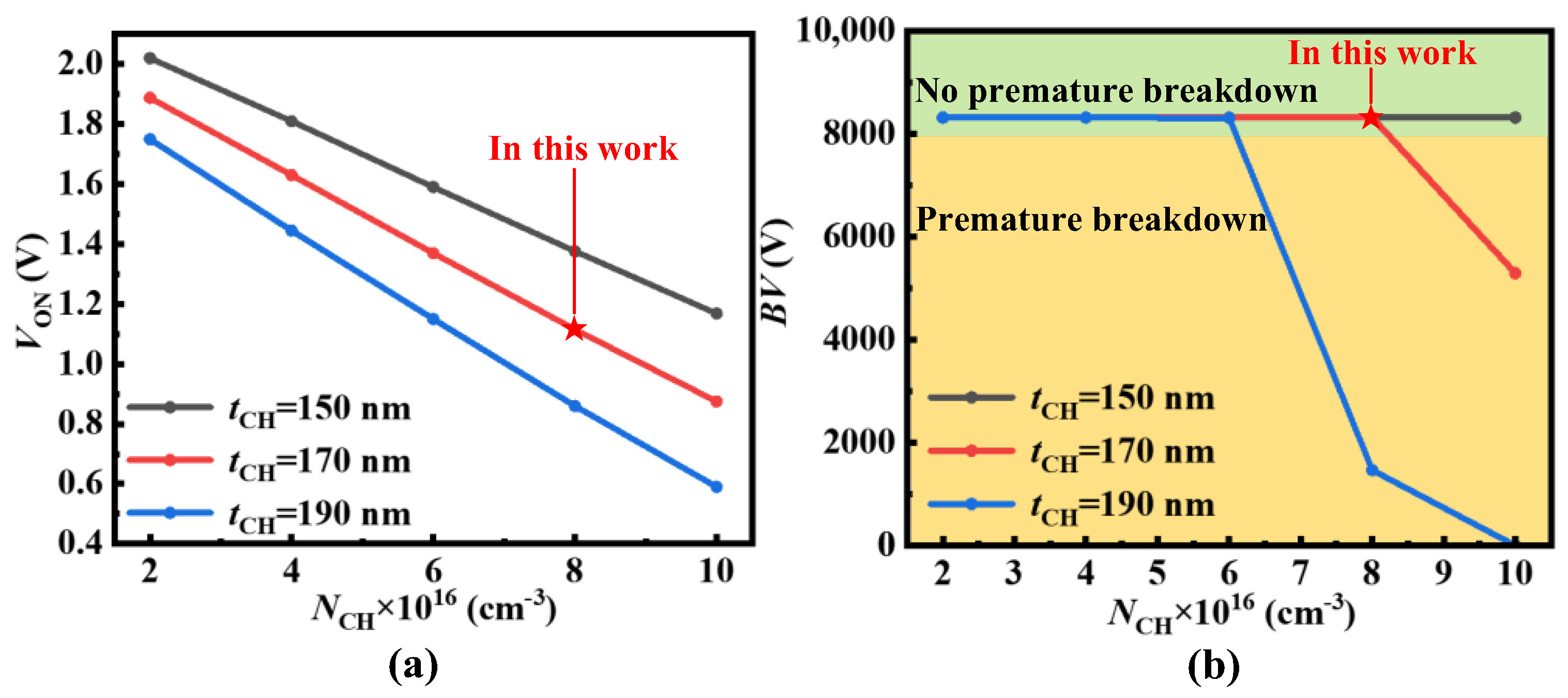
With the increase of tCH and NCH, the VON (@VGS = 0 V, IDS = −3 A/cm2) and BV (@IDS = 1 × 10⁻⁸ A/cm2) of UD-MOS decrease, as shown in Figure 5. It should be noted that the VON is mainly the voltage drop of the UD (i.e., VUD) and the thick epi-layer. The thicker tCH and higher NCH bring lower VON, but also lead to premature breakdown. Therefore, considering both the VON and BV of the UD-MOS, the tCH and NCH are designed to be 170 nm and 8 × 1016 cm−3, respectively. The key structural parameters of the C-MOS and UD-MOS are shown in Table 1.
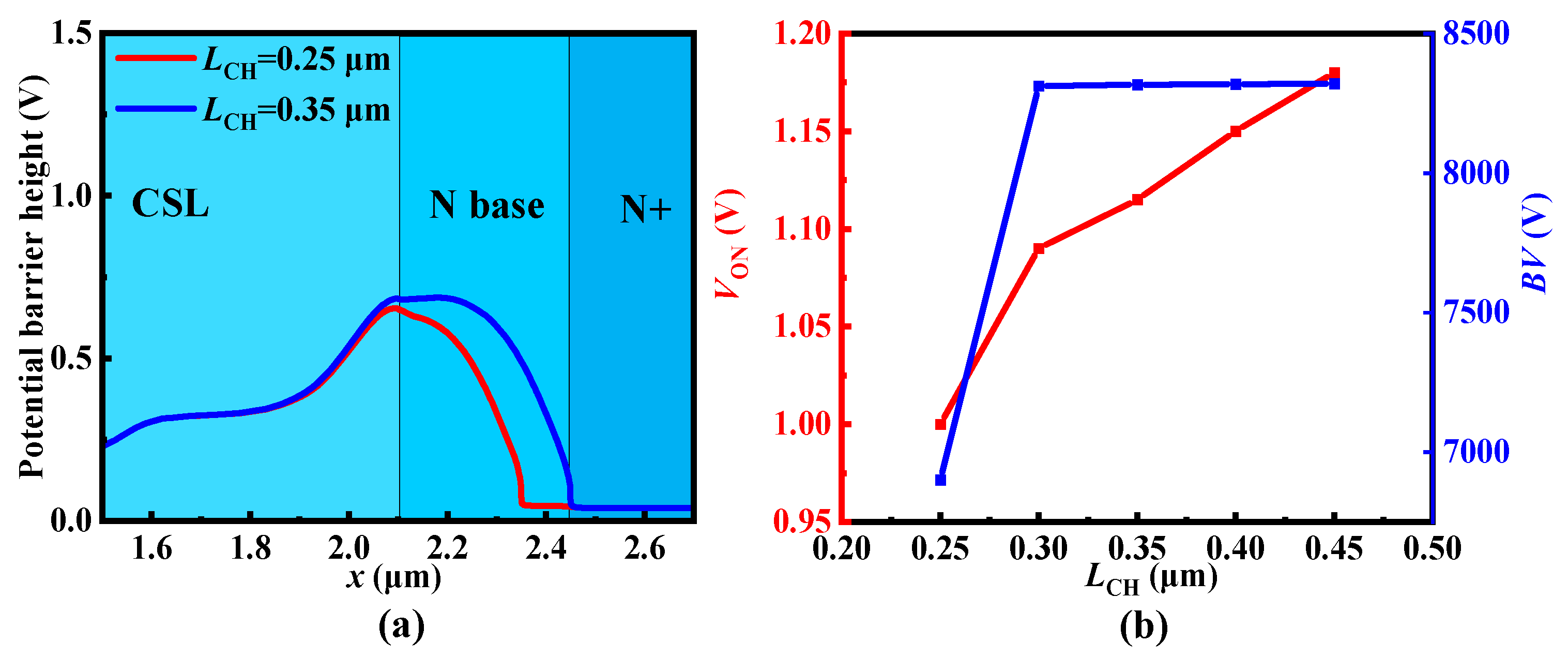
The effect of the N base length LCH on VUD is also discussed. With the narrowness of LCH, the potential of the N+ region influences the potential barrier of the N base as shown in Figure 6a. Although the lower VUD helps to reduce the VON, the BV is weakened at the same time, as shown in Figure 6b.

3.1. Static Characteristics

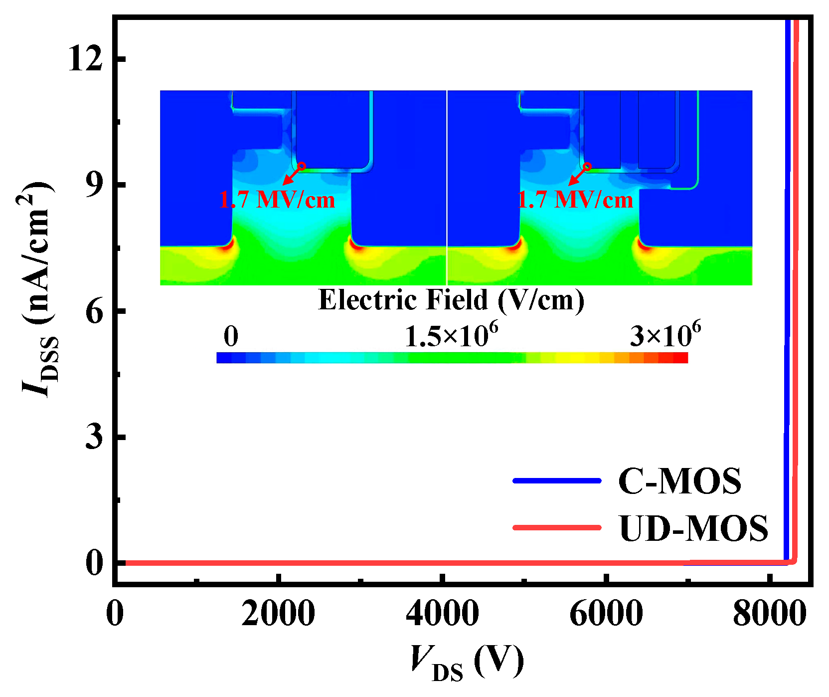
Based on optimized tCH and NCH, the SiC C-MOS and UD-MOS have a similar BV, as shown in Figure 7. The peak electric field in the gate oxide is less than 3 MV/cm, which ensures the long-term reliability of the gate oxide, as shown in the insets of Figure 7.
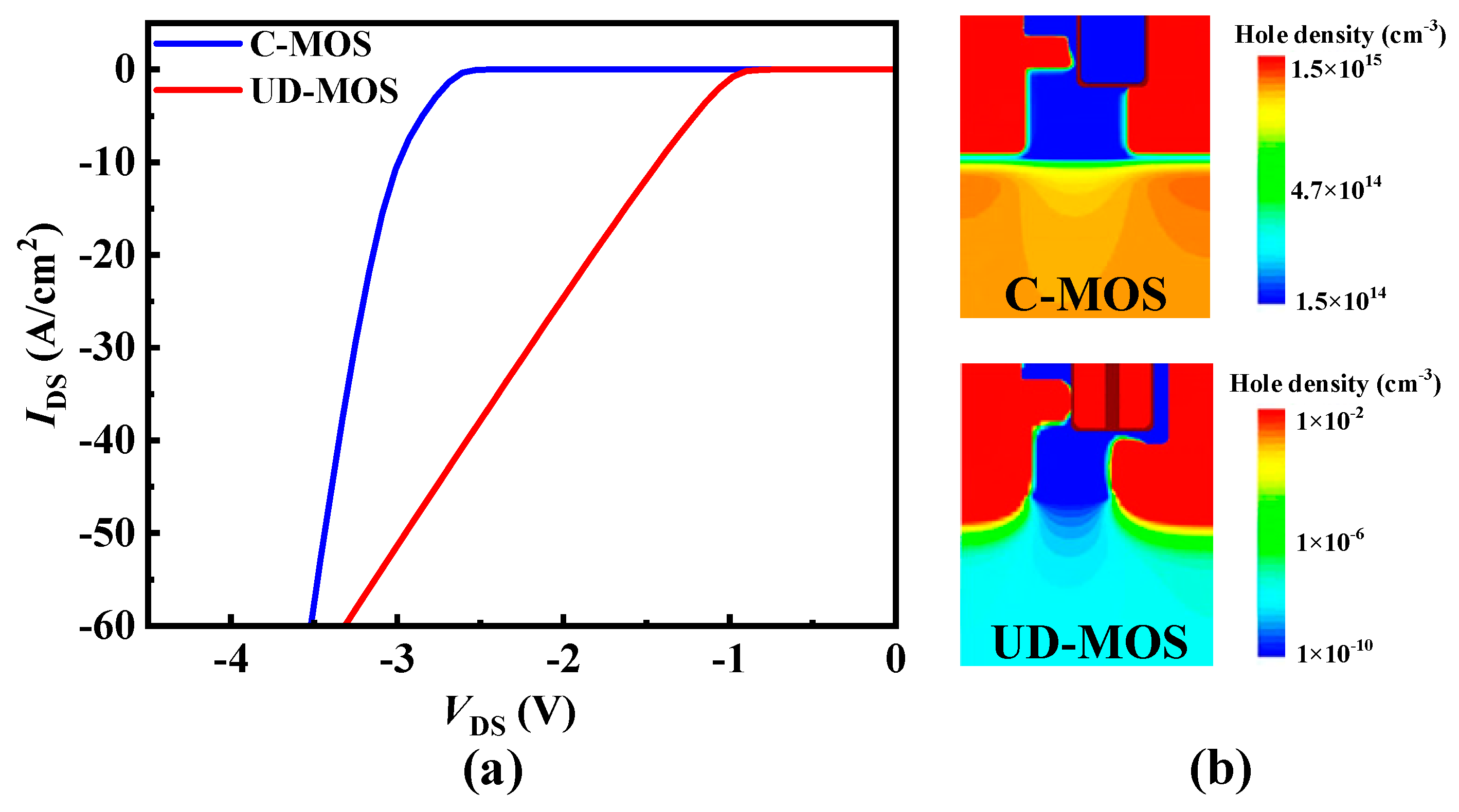
Moreover, the VON of UD-MOS is −1.1 V, while the C-MOS is −2.8 V, as shown in Figure 8a. It should be noted that the integrated unipolar diode makes for lesser hole injection into the drift region when in the reverse conduction condition, as shown in Figure 8b, which effectively avoids the risk of bipolar degradation.
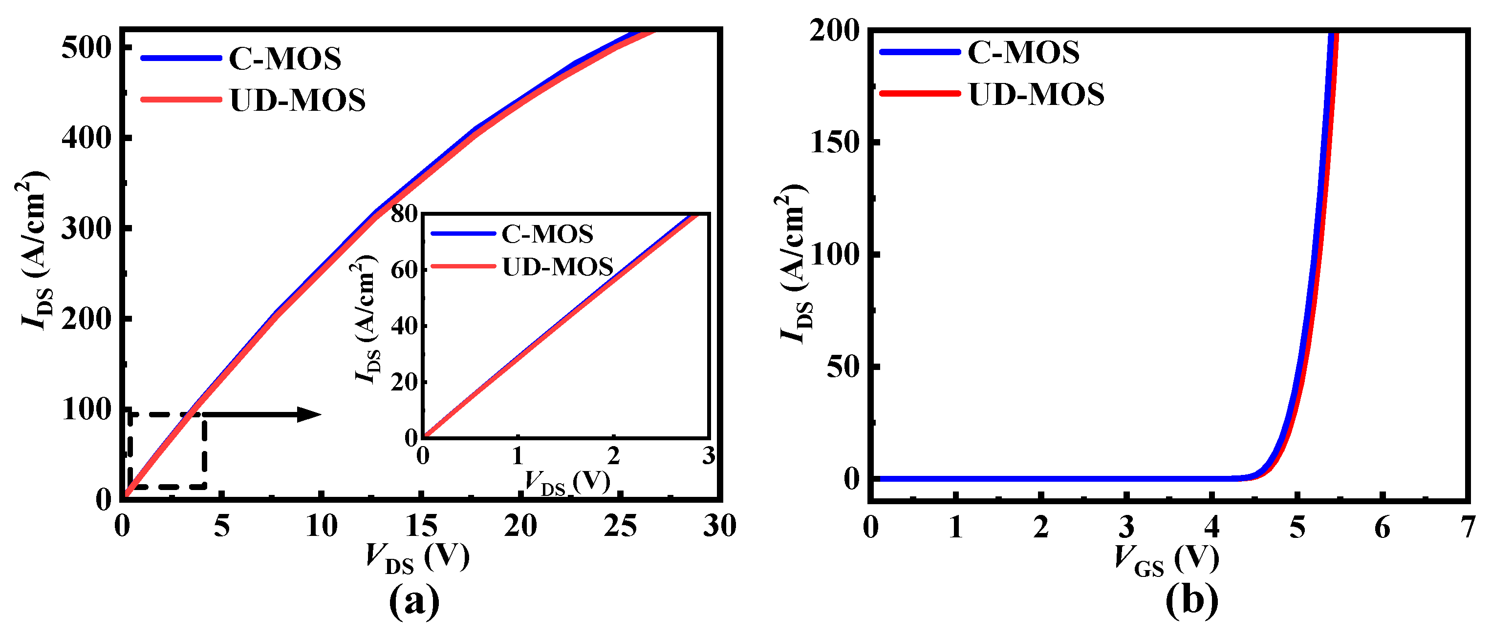
Even though the cell pitch of the UD-MOS is slightly larger than that of the C-MOS, the conduction capability of the UD-MOS is not degraded, because its channel density no longer dominates for high voltage SiC MOSFETs. The RON of UD-MOS and C-MOS are 35.48 mΩ·cm2 and 35.00 mΩ·cm2, respectively (@IDS = 50 A/cm2), as shown in Figure 9a. The transfer characteristic of the UD-MOS is also not degraded, which shows nearly the same VTH as the C-MOS, as shown in Figure 9b.

3.2. Dynamic Characteristics

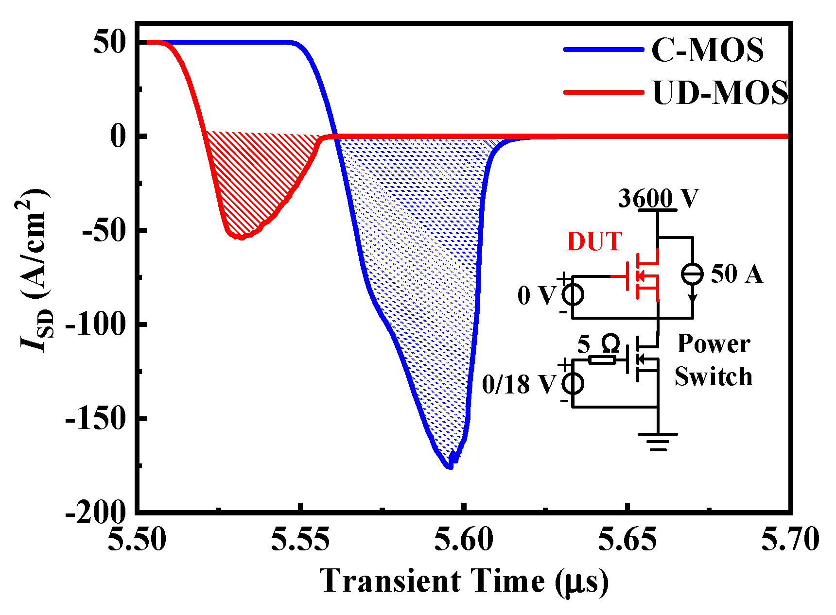
The reverse recovery characteristics of the body diode in the SiC C-MOS and UD-MOS are compared, as shown in Figure 10. Thanks to no extraction of minority carrier during the reverse recovery process, the peak reverse recovery current (IRRM) and reverse recovery charge (QRR) of UD-MOS are 54 A/cm2 and 1.04 μC/cm2, which are significantly reduced by 76% and 81%, respectively, compared to the C-MOS (IRRM =176 A/cm2 and QRR =5 μC/cm2).
Moreover, the dummy gate of the UD-MOS reduces the effective overlapping area between gate and drain terminals, so that the gate-to-drain capacitance (CGD) is 4.01 pF/cm2 (@VDS = 3600 V), which is reduced by 9.5% compared with the C-MOS. Meanwhile, due to the thick oxide layer between the trench gate and dummy gate as well as a slightly smaller overlapping area, the gate-to-source capacitance (CGS) of the UD-MOS is 18.1 nF/cm2, which is reduced by 52%. Accordingly, thanks to the smaller CGD and CGS, the UD-MOS has a lower gate charge (QG) of 566 nC/cm2 (@VGS = 0 V–18 V) and gate-to-drain charge (QGD) of 109 nC/cm2, as shown in Figure 11. Furthermore, considering conduction and dynamic capability, the UD-MOS exhibits a better loss-related figure of merit (FOM, i.e., RON × QGD [21]) of 3.87 mΩ·μC, which is 8.7% lower than that of the C-MOS.
The switching waveforms of the SiC C-MOS and DP-MOS are as shown in Figure 12. Benefitting from the reduced capacitances, the UD-MOS has lower turn-on loss (EON) and turn-off loss (EOFF) of 3.80 mJ/cm2 and 3.36 mJ/cm2, which are 34% and 17% lower than that of the C-MOS, respectively.
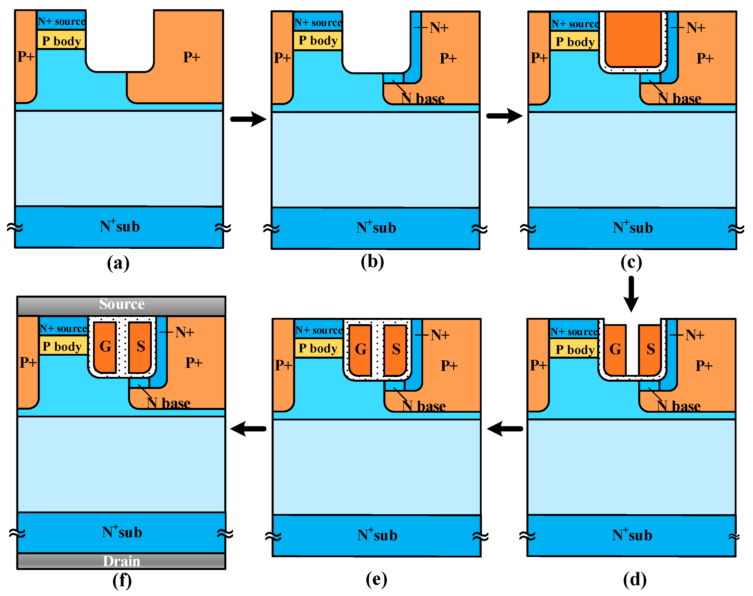
One feasible process flow of the UD-MOS is presented, including (a) epitaxial growing, P body implantation, N+ source region implantation, trench etch and P+ region implantation, (b) N+ region and N base region implantation, (c) thermal oxidation and polysilicon gate deposition, (d) polysilicon etch, (e) isolated oxidation deposition and (f) metallization, as shown in Figure 13. Finally, Table 2 compares the main characteristics of the SiC UD-MOS and the C-MOS. The SiC UD-MOS exhibits superior performance due to the unipolar diode.

4. Conclusions

A novel 6500 V SiC trench UD-MOS is proposed with improved reverse conduction and switching characteristics. The grounded dummy gate causes the unipolar diode of the SiC UD-MOS to reduce VON to 1.1 V, which avoids the risk of bipolar degradation and reduces the parasitic capacitances with lower switching loss. The proposed UD-MOS provides a promising device prototype in VSC applications for HVDC transmission.

Author Contributions

Writing—original draft preparation, H.W.; writing—review, editing, and instruction, X.L.; methodology, X.D.; software, Y.W. and J.D.; validation, W.P.; supervision, B.Z. All authors have read and agreed to the published version of the manuscript.

Funding

This research was supported in part by the National Natural Science Foundation of China under Grant No. 62004033 and 62274025, in part by the Sichuan Science and Technology Program No. 2022YFQ0096 and 2022YFQ0103, in part by the Science and Technology Project of State Grid Corporation of China under Grant 5500-202158437A-0-0-00.

Data Availability Statement

Data are contained within the article.

Conflicts of Interest

The authors declare no conflict of interest.

References

  1. Spaziani, L.; Lu, L. Silicon, GaN and SiC: There’s room for all: An application space overview of device considerations. In Proceedings of the 2018 IEEE 30th International Symposium on Power Semiconductor Devices and ICs (ISPSD), Chicago, IL, USA, 13–17 May 2018; pp. 8–11. [Google Scholar] [CrossRef]
  2. Ghosh, R.; Mondal, S.; Ghorui, S.K. SiC MOSFET Based VSC Used in HVDC Transmission with DC Fault Protection Scheme. In Proceedings of the2017 International Conference on Computer, Electrical & Communication Engineering (ICCECE), Kolkata, India, 22–23 December 2017; pp. 1–5. [Google Scholar] [CrossRef]
  3. Li, X.; Jiang, J.; Huang, A.Q.; Guo, S.; Deng, X.; Zhang, B.; She, X. A SiC Power MOSFET Loss Model Suitable for High-Frequency Applications. IEEE Trans. Ind. Electron. 2017, 64, 8268–8276. [Google Scholar] [CrossRef]
  4. Kimoto, T.; Iijima, A.; Tsuchida, H.; Miyazawa, T.; Tawara, T.; Otsuki, A.; Kato, T.; Yonezawa, Y. Understanding and reduction of degradation phenomena in SiC power devices. In Proceedings of the 2017 IEEE International Reliability Physics Symposium (IRPS), Monterey, CA, USA, 2–6 April 2017; IEEE: Piscataway, NJ, USA, 2017; pp. 2A-1.1–2A-1.7. [Google Scholar]
  5. Agarwal, A.; Fatima, H.; Haney, S.; Ryu, S.-H. A New Degradation Mechanism in High-Voltage SiC Power MOSFETs. IEEE Electron. Device Lett. 2007, 28, 587–589. [Google Scholar] [CrossRef]
  6. Ishigaki, T.; Murata, T.; Kinoshita, K.; Morikawa, T.; Oda, T.; Fujita, R.; Konishi, K.; Mori, Y.; Shima, A. Analysis of Degradation Phenomena in Bipolar Degradation Screening Process for SiC-MOSFETs. In Proceedings of the 2019 31st International Symposium on Power Semiconductor Devices and ICs (ISPSD), Shanghai, China, 19–23 May 2019; pp. 259–262. [Google Scholar] [CrossRef]
  7. Jiang, H.; Wei, J.; Dai, X.; Zheng, C.; Ke, M.; Deng, X.; Sharma, Y.; Deviny, I.; Mawby, P. SiC MOSFET with built-in SBD for reduction of reverse recovery charge and switching loss in 10-kV applications. In Proceedings of the 2017 29th International Symposium on Power Semiconductor Devices and IC’s (ISPSD), Sapporo, Japan, 28 May–1 June 2017; pp. 49–52. [Google Scholar] [CrossRef]
  8. Saito, K.; Miyoshi, T.; Kawase, D.; Hayakawa, S.; Masuda, T.; Sasajima, Y. Simplified Model Analysis of Self-Excited Oscillation and Its Suppression in a High-Voltage Common Package for Si-IGBT and SiC-MOS. IEEE Trans. Electron. Devices 2018, 65, 1063–1071. [Google Scholar] [CrossRef]
  9. Sung, W.; Baliga, B.J. On developing one-chip integration of 1.2 kV SiC MOSFET and JBS diode (JBSFET). IEEE Trans. Ind. Electron. 2017, 64, 8206–8212. [Google Scholar] [CrossRef]
  10. Sundaresan, S.; Park, J.; Mulpuri, V.; Singh, R. Performance and Robustness of 6500 V SiC DMOSFETs with Integrated MPS diodes. In Proceedings of the 2021 33rd International Symposium on Power Semiconductor Devices and ICs (ISPSD), Nagoya, Japan, 30 May–3 June 2021; pp. 235–238. [Google Scholar] [CrossRef]
  11. Kawahara, K.; Hino, S.; Sadamatsu, K.; Nakao, Y.; Yamashiro, Y.; Yamamoto, Y.; Iwamatsu, T.; Nakata, S.; Tomohisa, S.; Yamakawa, S. 6.5 kV schottky-barrier-diode-embedded SiC-MOSFET for compact full-unipolar module. In Proceedings of the 2017 29th International Symposium on Power Semiconductor Devices and IC’s (ISPSD), Sapporo, Japan, 28 May–1 June 2017; pp. 41–44. [Google Scholar] [CrossRef]
  12. Zhou, X.; Pang, H.; Jia, Y.; Hu, D.; Wu, Y.; Tang, Y.; Xia, T.; Gong, H.; Zhao, Y. SiC Double-Trench MOSFETs With Embedded MOS-Channel Diode. IEEE Trans. Electron. Devices 2020, 67, 582–587. [Google Scholar] [CrossRef]
  13. Zhou, X.; Gong, H.; Jia, Y.; Hu, D.; Wu, Y.; Xia, T.; Pang, H.; Zhao, Y. SiC Planar MOSFETs With Built-In Reverse MOS-Channel Diode for Enhanced Performance. IEEE J. Electron. Devices Soc. 2020, 8, 619–625. [Google Scholar] [CrossRef]
  14. Zhu, L.; Chow, T.; Jones, K.; Agarwal, A. Design, fabrication, and characterization of low forward drop, low leakage, 1-kV 4H-SiC JBS rectifiers. IEEE Trans. Electron. Devices 2006, 53, 363–368. [Google Scholar] [CrossRef]
  15. Bodeker, C.; Vogt, T.; Silber, D.; Kaminski, N. Criterion for the Stability Against Thermal Runaway During Blocking Operation and Its Application to SiC Diodes. IEEE J. Emerg. Sel. Top. Power Electron. 2016, 4, 970–977. [Google Scholar] [CrossRef]
  16. Li, X.; Tong, X.; Huang, A.Q.; Tao, H.; Zhou, K.; Jiang, Y.; Jiang, J.; Deng, X.; She, X.; Zhang, B.; et al. SiC Trench MOSFET with Integrated Self-Assembled Three-Level Protection Schottky Barrier Diode. IEEE Trans. Electron. Devices 2018, 65, 347–351. [Google Scholar] [CrossRef]
  17. Beier-Moebius, M.; Lutz, J. Breakdown of gate oxide of 1.2 kV SiC-MOSFETs under high temperature and high gate voltage. In Proceedings of the PCIM Europe 2016—International Exhibition and Conference for Power Electronics, Intelligent Motion, Renewable Energy and Energy Management, Nuremberg, Germany, 10–12 May 2016; pp. 1–8. [Google Scholar]
  18. Ohoka, A.; Uchida, M.; Kiyosawa, T.; Horikawa, N.; Saitou, K.; Kanzawa, Y.; Sorada, H.; Sawada, K.; Ueda, T. Reduction of RonA retaining high threshold voltage in SiC DioMOS by improved channel design. In Proceedings of the 2018 IEEE 30th International Symposium on Power Semiconductor Devices and ICs (ISPSD), Chicago, IL, USA, 13–17 May 2018; pp. 52–55. [Google Scholar] [CrossRef]
  19. Uchida, M.; Horikawa, N.; Tanaka, K.; Takahashi, K.; Kiyosawa, T.; Hayashi, M.; Niwayama, M.; Kusumoto, O.; Adachi, K.; Kudou, C.; et al. Novel SiC power MOSFET with integrated unipolar internal inverse MOS-channel diode. In Proceedings of the 2011 International Electron Devices Meeting, Washington, DC, USA, 5–7 December 2011; pp. 26.6.1–26.6.4. [Google Scholar] [CrossRef]
  20. Ohoka, A.; Horikawa, N.; Kiyosawa, T.; Sorada, H.; Uchida, M.; Kanzawa, Y.; Sawada, K.; Ueda, T.; Fujii, E. 40 mΩ/1700 V DioMOS (Diode in SiC MOSFET) for High Power Switching Applications. Mater. Sci. Forum 2014, 778–780, 911–914. [Google Scholar] [CrossRef]
  21. Huang, A. New Unipolar Switching Power Device Figures of Merit. IEEE Electron. Device Lett. 2004, 25, 298–301. [Google Scholar] [CrossRef]
Figure 1. Schematic cross-section view of the 6500 V SiC (a) C-MOS and (b) UD-MOS.
Micromachines 15 00092 g001
Figure 2. Potential barrier distribution at zero-bias (VGS = 0 V and VDS = 0 V) condition. (a) Along line A-A′ of the SiC C-MOS, (b) along line A-A′ of the SiC UD-MOS, (c) along line B-B′ of the SiC C-MOS, and (d) along line B-B′ of the SiC UD-MOS.
Micromachines 15 00092 g002
Figure 3. Potential barrier distribution along line B-B′ of the SiC UD-MOS. (a) The blocking condition and (b) the reverse conduction condition at VGS = 0 V.
Micromachines 15 00092 g003
Figure 4. Effects of (a) NCH and (b) tCH on the potential barrier height along line A-A′ at zero-bias condition (VGS = VDS = 0 V).
Micromachines 15 00092 g004
Figure 5. Effects of tCH and NCH on (a) VON and (b) BV of UD-MOS.
Micromachines 15 00092 g005
Figure 6. (a) Potential distribution in different LCH and (b) effect of LCH on VON and BV.
Micromachines 15 00092 g006
Figure 7. Blocking characteristics of the SiC C-MOS and UD-MOS. The insets show the electric field distributions in SiC MOSFET at VDS = 6500 V.
Micromachines 15 00092 g007
Figure 8. (a) Reverse conduction characteristics and (b) hole density distribution of the SiC C-MOS and UD-MOS at VGS = 0 V and ISD = 50 A/cm2.
Micromachines 15 00092 g008
Figure 9. (a) Output characteristics at VGS = 18 V and (b) transfer characteristics of the SiC C-MOS and UDMOS.
Micromachines 15 00092 g009
Figure 10. Reverse recovery characteristics of the body diode in the SiC C-MOS and UD-MOS.
Micromachines 15 00092 g010
Figure 11. (a) Capacitance characteristics at VGS = 0 V, f = 1 MHz and (b) QG for the SiC C-MOS and UD-MOS.
Micromachines 15 00092 g011
Figure 12. (a) Turn-on and (b) turn-off waveforms of the C-MOS and UD-MOS at VDS = 3600 V and IDS = 50 A/cm2.
Micromachines 15 00092 g012
Figure 13. Brief fabrication process flow of the SiC UD-MOS. (a) Epitaxial growing, P body implantation, N+ source region implantation, trench etch and P+ region implantation, (b) N+ region and N base region implantation, (c) thermal oxidation and polysilicon gate deposition, (d) polysilicon etch by oxide sidewall spacer, (e) isolated oxidation deposition and (f) metallization.
Micromachines 15 00092 g013
Table 1. Key Structure Parameters of the SiC C-MOS and UD-MOS.
ParametersUD-MOSC-MOS
cell pitch (μm)3.353.15
drift region thickness (μm)6060
drift region doping (cm−3)1.2 × 10151.2 × 1015
polysilicon width (μm)0.80.8
trench depth (μm)0.90.9
trench width (μm)1.10.9
oxide thickness (nm)5050
CSL doping (cm−3)3 × 10163 × 1016
JFET width (μm)1.31.3
P+ region thickness (μm)1.71.7
P+ region doping (cm−3)1 × 10191 × 1019
N base length (μm)0.35
N base thickness (nm)170
N base doping (cm−3)8 × 10¹⁶
Table 2. Performance Comparison of the SiC C-MOS and UD-MOS.
ParametersUD-MOSC-MOS
RON (mΩ·cm2)35.4834.99
VON (V)−1.11−2.77
BV (V)83178217
VTH (V)5.25.2
IRRM (A/cm2)54176
CGS (nF/cm2)18.137.9
CDS (pF/cm2)149149
CGD (pF/cm2)4.014.43
QRR (μC/cm2)1.225.01
QG (nC/cm2)566970
QGD (nC/cm2)109121
RON × QGD (mΩ·μC)3.874.24
EON (mJ/cm2)3.85.71
EOFF (mJ/cm2)3.364.38
Disclaimer/Publisher’s Note: The statements, opinions and data contained in all publications are solely those of the individual author(s) and contributor(s) and not of MDPI and/or the editor(s). MDPI and/or the editor(s) disclaim responsibility for any injury to people or property resulting from any ideas, methods, instructions or products referred to in the content.