Review

A Review of Ku-Band GaN HEMT Power Amplifiers Development

School of Electronic Engineering, Kyonggi University, Suwon-Si 16227, Republic of Korea
Micromachines 2024, 15(11), 1381; https://doi.org/10.3390/mi15111381
Submission received: 4 October 2024 / Revised: 11 November 2024 / Accepted: 14 November 2024 / Published: 15 November 2024

Abstract

:
This review article investigates the current status and advances in Ku-band gallium nitride (GaN) high-electron mobility transistor (HEMT) high-power amplifiers (HPAs), which are critical for satellite communications, unmanned aerial vehicle (UAV) systems, and military radar applications. The demand for high-frequency, high-power amplifiers is growing, driven by the global expansion of high-speed data communication and enhanced national security requirements. First, we compare the main GaN HEMT process technologies employed in Ku-band HPA development, categorizing the HPAs into monolithic microwave integrated circuits (MMICs) and internally matched power amplifier modules (IM-PAMs) and examining their respective characteristics. Then, by reviewing the literature, we explore design topologies, major issues like oscillation prevention and bias circuits, and heat sink technologies for thermal management. Our findings indicate that silicon carbide (SiC) substrates with gate lengths of 0.25 μm and 0.15 μm are predominantly used, with ongoing developments enabling MMICs and IM-PAMs to achieve up to 100 W output power and 30% power-added efficiency. Notably, the performance of MMIC power amplifiers is advancing more rapidly than that of IM-PAMs, highlighting MMICs as a promising direction for achieving higher efficiency and integration in future Ku-band applications. This paper can provide insights into the overall key technologies for Ku-band GaN HPA design and future development directions.

1. Introduction

In recent years, the demand for satellite communication services has increased not only in military applications but also in civilian ones, drawing significant attention to related technology development. Satellite communication technology enables communication between earth stations via satellites, providing various communication and broadcasting services [1,2,3]. Figure 1 shows the various applications of satellite communications [4]. Satellite communication can be classified into low, medium, and high orbits, including geostationary orbits, based on altitude. Geostationary satellite communication can cover the entire globe with just three satellites, offering the economic advantage of replacing numerous ground base stations for wide coverage. In contrast, low-orbit satellite communication provides high-speed communication with low latency. In particular, the recent Russian–Ukrainian war and the frequent occurrence of various disasters have highlighted the advantages of maintaining communication during emergencies and crises, leading to the emergence of private satellite communication companies such as Starlink. In addition to civilian communication services, there is a growing demand for satellite radar for military surveillance and reconnaissance. Amid the uncertainty of localized wars, not only developed countries like the United States, European Union, Japan, and China, but also nations worldwide are increasingly focused on developing satellite communication and radar technology for national security [5,6].
The frequency bands used for satellite communications are primarily divided into C-band, X-band, Ku-band, and Ka-band. Among these, Ku-band and Ka-band offer advantages such as supporting large data transmission, providing high-resolution services with wide bandwidth, and enabling antenna miniaturization due to their shorter wavelengths [4]. However, due to the high operating frequency, the performance of transceiver modules used in towers and earth stations has been limited, making development challenging. Recent advances in complementary metal–oxide–semiconductor (CMOS) and gallium nitride (GaN) high-electron mobility transistor (HEMT) semiconductor process technology have, however, enabled commercialization. Ku-band is now used not only for satellite communication but also in transmitter and receiver modules (TRMs) for unmanned aerial vehicle (UAV) communication, which is increasingly being utilized alongside satellites due to its advantages in miniaturization and bandwidth [7].
Table 1 compares the electrical properties of major semiconductor materials [8], while Figure 2 illustrates the breakdown voltage characteristics as a function of cutoff frequency for semiconductor devices [9,10]. As shown in Table 1 and Figure 2, GaN HEMT semiconductors have been widely studied and commercialized as high-frequency power semiconductors due to their high breakdown voltage and excellent electron mobility stemming from their wide energy band gap. High-power amplifiers (HPAs) present significant challenges in achieving performance in Ku-band satellite and UAV TRMs. To attain high output power, traveling wave tube amplifiers (TWTAs), which utilize vacuum tube technology, have traditionally been employed; however, they are heavy and unstable due to their high-voltage operation. Now, advances in GaN HEMT semiconductor process technology are enabling the replacement of conventional TWTAs with solid-state power amplifiers (SSPAs) [11,12].
In line with this trend, research on Ku-band GaN HEMT HPAs has been actively conducted by various research groups worldwide. This paper aims to summarize the current status and major issues related to Ku-band GaN HEMT HPA technology developed in recent years. The paper is organized as follows: In Section 2.1, we compare the processes used to implement Ku-band GaN HEMT HPAs; in Section 2.2, we discuss the two main approaches to implementing HPAs—monolithic microwave integrated circuits (MMICs) and internally matched power amplifier modules (IM-PAMs)—and examine their respective high-power design strategies and key issues. In Section 2.3, we review research on additional performance enhancements beyond high power, and finally, we provide conclusions.

2. Ku-Band GaN HEMT HPA Technology

2.1. GaN HEMT Process

To realize a GaN HEMT power amplifier, it is essential to develop a GaN HEMT process that provides the necessary design kits and fabricates the circuits or devices. Figure 3 shows the cross-sectional structure of a typical GaN HEMT [13]. GaN HEMTs with high cutoff frequency (fT) and maximum oscillation frequency (fMAX) are required, as obtaining gain becomes more challenging with increasing operating frequency. Therefore, the gate length of the transistor needs to be reduced according to the scaling rule. In this case, the breakdown voltage is also reduced proportionally, which can be a disadvantage in power amplifier design. The substrate material is also an important factor in the choice of process. Generally, GaN HEMT processes are divided into two types: those using silicon carbide (SiC) substrates and those using silicon (Si) substrates. SiC substrates have high thermal conductivity, which is beneficial for dissipating heat generated by self-heating due to the high power density of GaN HEMTs. Therefore, they are often used in the process for GaN HEMT HPAs. However, SiC is hard and difficult to process during post-processing tasks such as dicing. In contrast, Si substrates are easier to produce using mature silicon-based semiconductor technology, are simpler to process, and are more amenable to mass production, providing significant economic advantages. However, they have relatively poor thermal conductivity and are more susceptible to self-heating effects.
The most commonly used processes for GaN HEMT HPAs are the 0.15 μm and 0.25 μm GaN HEMT processes. Here, 0.15 μm and 0.25 μm refer to the gate lengths of GaN HEMT devices. To achieve the required gain for power amplification in Ku-band, GaN HEMTs with gate lengths of 0.25 μm or less are preferred. Recently, 0.15 μm processes have become more popular due to their ability to achieve a high gain and high power added efficiency. Table 2 compares the device and process information for the commercial 0.25-μm GaN HEMT process, while Table 3 compares the device and process information for the commercial 0.15-μm GaN HEMT process.
Most commercial foundries still use SiC substrates, with the exceptions of MACOM/France (formerly OMMIC) and GCS. The 0.25 μm process is based on a drain voltage of 28–30 V. Recently, GaN HEMT processes have been developed to operate at higher voltages of 40–50 V, depending on the foundry, leading to a nearly twofold increase in power density. However, the fT is only 23 to 32 GHz, which can limit power gain at high edge frequencies in the Ku-band. Breakdown voltages range from 75 to 200 V. Meanwhile, the 0.15 μm process utilizes a somewhat lower drain voltage of 20 to 28 V compared with the 0.25 μm process, with a minimum of 12 V for OMMICs using Si substrates. Breakdown voltages for this process range from 50 to 120 V. The lower drain voltage reduces the voltage swing of the power amplifier, which is a disadvantage for achieving high output power. However, the fT performance, which is two to three times higher than that of the 0.25 μm process, is favorable for obtaining high power gain and improving efficiency. As shown in Table 3, the power-added efficiency (PAE) of over 50% at 30 GHz led to the expectation of better power efficiency compared with the 0.25 μm process in the Ku-band. MACOM/France (formerly OMMIC)‘s GaN-on-Si HEMT process has shown output power performance comparable to other processes, even with a drive voltage of 12 V. HPA designs using cascode or stacked-field effect transistor (FET) structures that enhance the voltage swing in this process are expected to yield higher output power and warrant further research [21,22].

2.2. High Power Amplifier Design

There are two main ways to implement HPAs. The first is the MMIC type, where both transistors and input/output matching circuits are designed and fabricated within a single integrated circuit [23,24,25,26,27,28,29,30,31,32,33,34,35,36]. This approach reduces the overall circuit size, facilitates mass production, and significantly minimizes parasitic components generated by the connection between the transistor and the matching circuits [20,37]. However, achieving a high dielectric constant ( ε r ) is challenging with conventional semiconductor processes, making it difficult to use high-Q inductors. Additionally, employing passive elements with large inductance (L) or capacitance (C) values for matching and bias circuits increases costs due to the larger chip size.
The second method is the microwave integrated circuit (MIC) or hybrid type, which utilizes packaged transistors while implementing the input/output matching circuit on the printed circuit board (PCB) [37]. This method leverages PCBs with low losses and high dielectric constants to reduce matching losses by using high-Q inductors and allows for the use of large inductors and capacitors. It also offers the advantage of being tunable after fabrication, enabling easy modifications and optimizations [37]. However, this method results in a bulkier overall circuit size, and matching is limited due to parasitic components caused by wire bonding when connecting the transistor and the matching circuit [37,38]. As frequency increases, the impact of these parasitic components becomes more significant, degrading performance. To address this, the internally matched HPA design is often used, incorporating matching circuitry within the packaged transistors [39,40,41,42,43,44,45,46,47].
Table 4 summarizes the key performance characteristics of reported Ku-band GaN HEMT HPA MMICs. As shown in Table 4, Ku-band power amplifier MMICs have been implemented on silicon and silicon carbide substrates, with output power ranging from 7.2 W to 93 W and gate lengths from 0.1 μm to 0.25 μm. Notably, several papers using the 0.15 μm process have demonstrated output powers exceeding 40 W while achieving power-added efficiencies (PAEs) of 30–40% [24,36]. In references [29,30], high efficiencies close to 40% were also reported at output powers above 10 W. GaN HEMT HPAs implemented with 0.25 μm processes exhibit somewhat lower power efficiency but achieve high output powers of over 40 W, as seen in references [28,32]. A recent paper [31] utilized a 0.2 μm internal process to achieve output power close to 100 W in MMIC form. This demonstrates that MMIC technology has advanced to the point where it can achieve performance comparable to that of existing IM-PAMs, and it is expected to replace TWTAs in the Ku-band.
Table 5 compares HPA MMIC papers with output powers exceeding 20 W from a circuit design perspective. All references adopted a multistage amplifier approach. Except for [32], which was designed as a four-stage amplifier, the other references used a three-stage configuration to drive the main power cell. For output powers up to 20 W, the main power cell combined the currents of eight GaN HEMTs in parallel, resulting in a total gate width of approximately 10 mm. For output powers above 40 W, the standard design approach employed sixteen GaN HEMTs in parallel, with a total gate width ranging from 10 to 25 mm. Notably, Ref. [31] presents a power cell with a total gate width of about 10 mm that achieved an output power of nearly 100 W, demonstrating excellent power density.
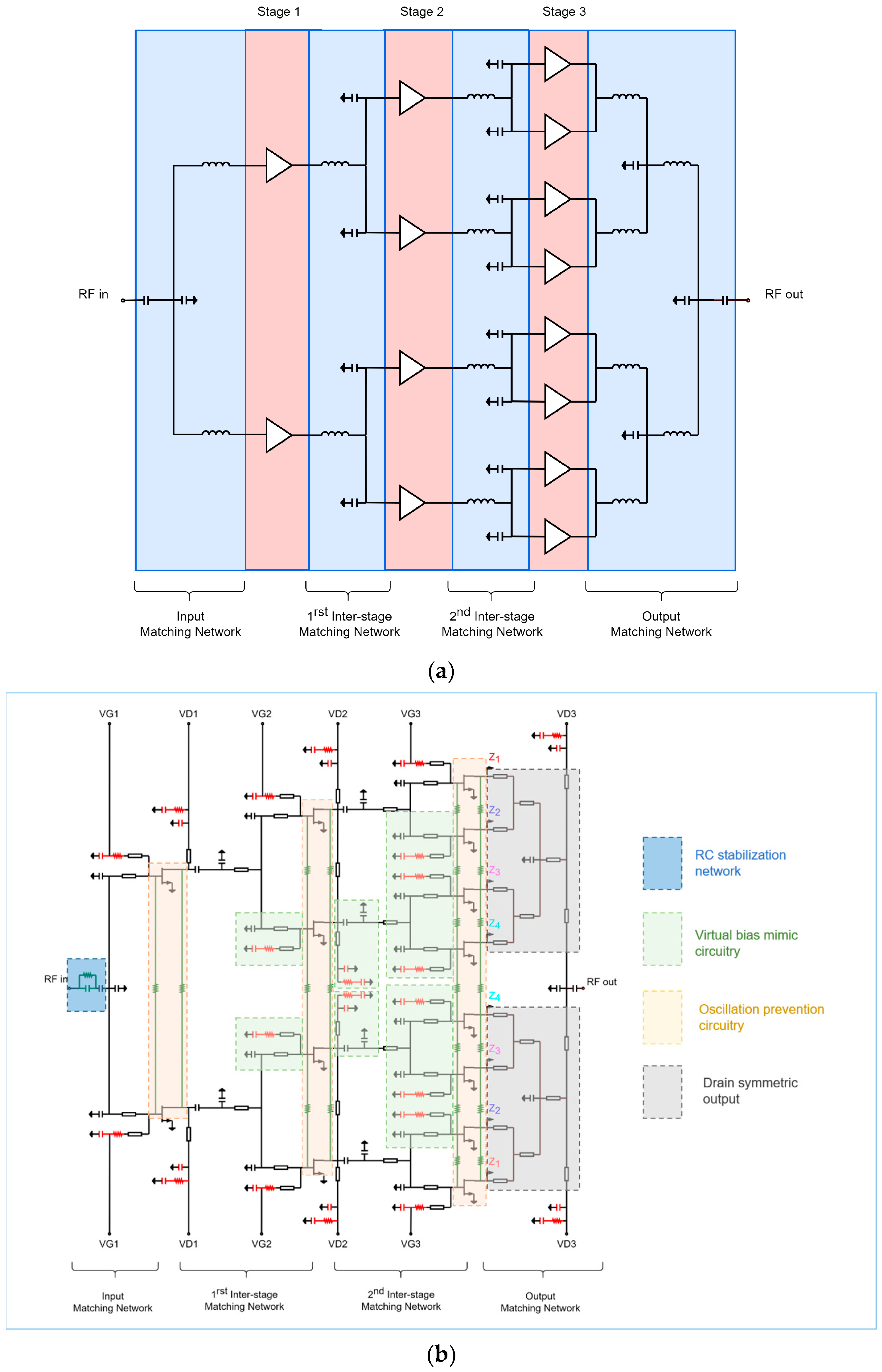
Figure 4a,b show the HPA structure and schematic commonly used in the aforementioned papers. The HPA consists of a two-way GaN HEMT power cell in the first stage, a four-way configuration in the second stage, and an eight-way configuration in the third stage. In contrast, an HPA with a 16-way GaN HEMT as the main power cell replicates the previously described 2-4-8 structure, tying the inputs and outputs together.
As shown in the schematic of Figure 4b, an RC stabilization circuit with resistors and capacitors connected in parallel is often employed to enhance the stability of the input side of the circuit. Due to the large size of the transistor, substantial DC currents and RF signals are input and output. This increases the risk of oscillation, particularly if the signal diverges to one side. To mitigate even-mode and odd-mode oscillations, large resistors are typically connected to the gate and drain (see the beige boxes in Figure 4b) [48].
Another design consideration is the source via the structure of the GaN HEMT. There are two main types of source vias: the outer source via (OSV), where only the outermost part of the source finger is connected, and the individual source via (ISV), which connects ground vias for each of the source fingers. Figure 5a,b illustrate the layouts of a 4 × 50 μm GaN HEMT device implemented in OSV and ISV configurations, respectively. In general, larger and more numerous ground source vias reduce the parasitic inductance caused by the source via structure, which improves load-pull characteristics and enhances device performance by dissipating heat generated by self-heating more effectively. However, the ISV structure can excessively increase the size of the main power cell, posing challenges for MMIC manufacturing. Therefore, it is common to use an ISV structure for the drive stage and an OSV for the main stage [32].
Additionally, careful design is essential for the bias circuit. As shown in Figure 4b, a virtual bias mimic circuit with open stubs and RCs in series on the opposite side of the actual bias input is used to ensure that each connected transistor presents the same impedance to the gate bias supply (see the green boxes in Figure 4b). The drain bias circuit also requires careful design to ensure that each transistor receives a drain voltage through a line that is in phase with the others (see the gray boxes in Figure 4b).
Table 6 compares Ku-band GaN HEMT HPAs implemented using the MIC approach. Compared with the MMIC schemes in Table 4, more 0.25 μm processes were utilized, with the average output power ranging from 50 to 120 W, which was higher than that of the MMIC schemes. However, the PAEs fell within the 20 to 30 percent range. All MIC power amplifiers in Table 6 were implemented in the IM-PAM type.
Table 7 compares the HPA MIC references of Table 6 from a circuit design perspective. The GaN dies used in the surveyed papers were primarily the CGHV1J070D, sold by MACOM (formerly Wolfspeed), and one developed in-house by Mitsubishi, Japan. The number of GaN HEMTs in the main power stage varied from 12 to 64, depending on the output power, with a total gate width approximately in the range of 15 to 30 mm. It is evident that MIC power amplifiers are primarily developed to achieve high output power in a narrow band. Due to the size constraints imposed by PCB implementation of input–output matching circuits, a single-stage design was often utilized, which necessitates a separate high-input driving power in the system configuration.
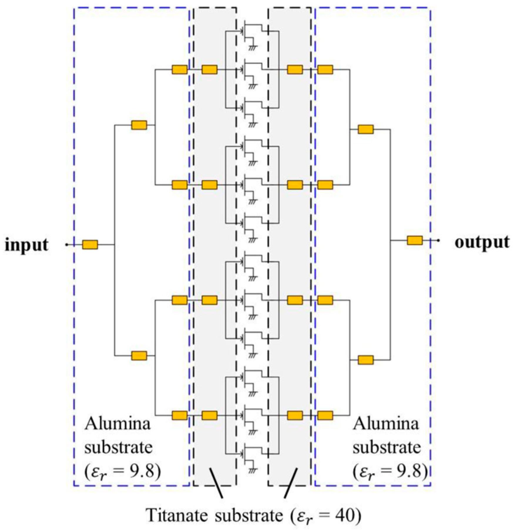
Figure 6 illustrates a typical example of a Ku-band MIC power amplifier implemented using an internal matching approach. To compactly implement an impedance transformer that transformed the low impedance of a large GaN HEMT die into a high impedance, the PCB connected to the GaN HEMT die was made from a material with a very high dielectric constant, as shown in Figure 6. This design prevented the feeding line widths from becoming excessively large, keeping the overall module size manageable. The power dividing and combining components that followed were implemented using materials with lower dielectric constants. In [41], PCBs with ε r values of 38.5 and 9.8 were used, while [43] also utilized PCBs with ε r values of 40 and 9.8. When transforming impedance, it is common to employ a multi-step impedance conversion to achieve a gradual transition and avoid a high Q-factor on the Smith chart [43].
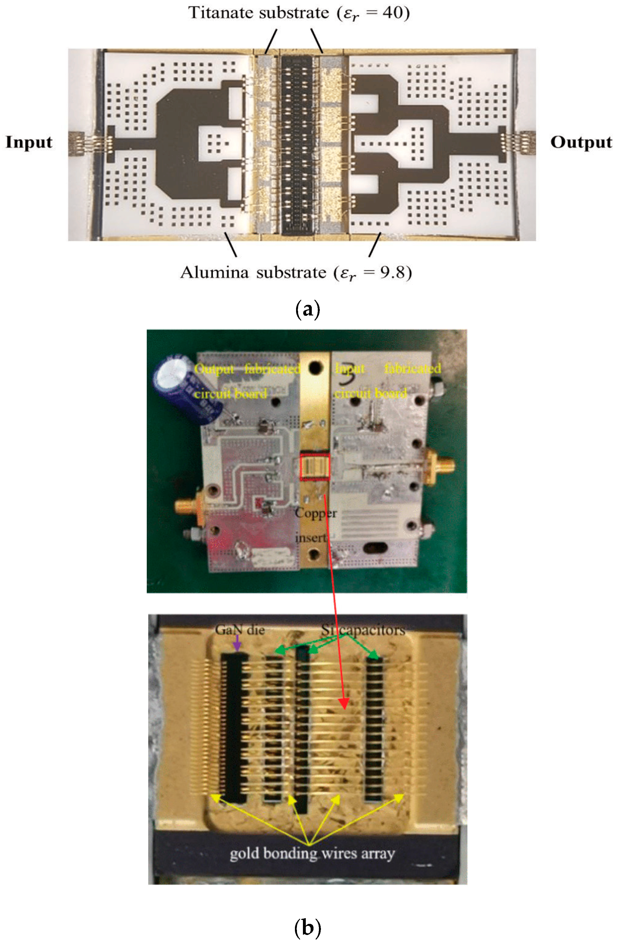
Additionally, the GaN HEMT die and PCB were connected via wire bonding, and this was advantageous to minimize the bonding length and maximize the number of bonds to reduce parasitic inductance. Figure 7a shows an example photograph of an actual fabricated Ku-band GaN HEMT IM-PAM, and Figure 7b presents a photo of a GaN HEMT power amplifier module featuring extensive wire bonding.
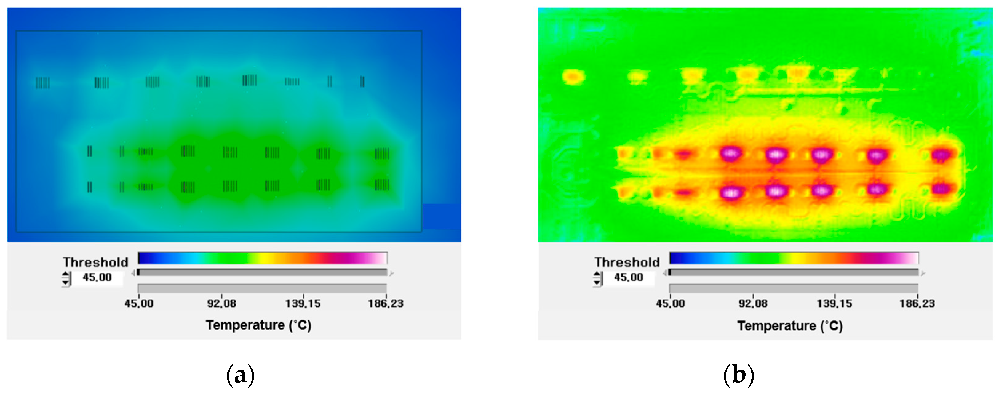
On the other hand, packaging and die attach technology that effectively dissipates heat is critical for achieving large output powers of 50 W or more. Figure 8a,b display the temperature distribution of a 20 W class GaN HEMT HPA bare die, with only DC power applied and with both DC and RF power applied, using a high-resolution infrared (IR) scope. It is evident that the maximum temperature nearly doubled from 90 °C to over 180 °C when RF power was applied near the center channel of the transistor, highlighting the necessity for effective heat dissipation techniques during the packaging process.
Table 8 compares the thermal conductivity of heat spreader materials commonly used in die attach. Table 9 summarizes the thermal conductivity of materials utilized as heat sinks or thermal interfaces. Several studies have employed eutectic die attachments with good thermal conductivity, mounting them on Cu-Mo-Cu flanges, which serve as excellent heat sinks, rather than the typical copper jig [44]. Figure 9 illustrates the heat sink structure of a GaN HEMT die, frequently used in IM-PAMs. Reference [49] reports improvements in output power and PAE by using chemical vapor deposition (CVD) diamond materials, which possess the best thermal conductivity, as the thermal interface on top of the copper heat sink, as shown in Figure 10.
In this subsection, we investigated two methods for implementing Ku-band GaN HEMT HPAs, MMICs and internally matched MIC design methods, by comparing the reported papers. As mentioned above, MMIC HPAs can be configured in a multistage arrangement with a compact size to achieve high gain, offering a low input power burden and wide bandwidth. In contrast, MIC HPAs are advantageous for obtaining high output power within a narrow bandwidth; however, due to size constraints, they are typically limited to a single-stage configuration and require high input power. Nonetheless, advancements in MMIC processes and design technologies have been significant in recent years, suggesting that we can expect numerous studies reporting output powers exceeding 100 W in the near future, such as in [31].

2.3. Other Additional Design Techniques

Ku-band GaN HEMT power amplifiers have been extensively studied to achieve high output power as a replacement for TWTAs. However, several research groups have conducted and published studies aimed at improving performance beyond just output power.
To enhance linearity, some researchers have embedded linearizers within the MMIC or designed separate linearizer modules in front of the MIC [23,47]. In [23], a linearizer composed of a simple diode and the inductance of a microstrip line was placed between the buffer and the power amplifier, resulting in an increase of 5 dB in linear output power with third-order intermodulation distortion (IMD3) levels below −25 dBc. In [47], a linearizer using two diodes, a bandpass filter (BPF), and microstrip lines was designed for the front end of the entire system, including the MIC power amplifier, improving amplitude modulation to amplitude modulation (AMAM) and amplitude modulation to phase modulation (AMPM) by 2 dB and 5 degrees, respectively.
In addition to linearity, a Doherty power amplifier was employed in [50] to increase backoff efficiency for telecommunication systems, achieving drain efficiencies exceeding 28% at 6 dB backoff power. In [25], a control circuit for load modulation was integrated into a balanced power amplifier design, resulting in 10–16 W output power and a high power-added efficiency (PAE) of 25–40% across the 6–18 GHz band, including Ku-band.
With the expansion of Ku-band satellite communication and UAV communication services, further research is anticipated to improve the linearity and efficiency of Ku-band GaN HEMT power amplifiers while maintaining high output power.

3. Conclusions

This article reviews the current state of Ku-band GaN HEMT high-power amplifiers for satellite communications, which are actively being developed and researched. Recent MMIC designs focus on GaN HEMT processes with gate lengths less than 0.2 μm on SiC substrates, achieving PAEs exceeding 30% and output powers nearing 100 W. Utilizing advanced heat dissipation packaging from MIC design, Ku-band GaN HEMT amplifiers are anticipated to expand into both GaN-on-SiC and cost-effective GaN-on-Si MMICs. Future developments will focus on enhancing linearity, backoff efficiency, and bandwidth to support applications in military and civilian satellite and UAV communications. Additionally, advancements in power efficiency, thermal management, and miniaturization will enable broader adoption across mobile and satellite platforms, with new markets like 5G/6G expected to drive commercial and defense applications. These trends underscore the ongoing importance of research in Ku-band GaN HEMT HPA technology.

Funding

The EDA tool was supported by the IC Design Education Center (IDEC), Korea.

Acknowledgments

I would like to express my gratitude to Electronic Device Solution Inc. for the industry–university connection with this research. I would like to express my sincere gratitude to Junghyun Kim and Hyosung Nam of Hanyang University for their invaluable assistance with my research and experiments. I also would like to express my sincere gratitude to Jaeku Ryu, Wireless Protocol Engineer at Amarisoft and the author of the Sharetechnote website, for his permission to cite useful illustrations about satellite communication. I would also like to thank the authors of the many references cited in this paper for their figures, data, and expertise.

Conflicts of Interest

The author declares no conflicts of interest.

References

  1. Nabeel, M.I.; Singh, K.; Afzal, M.U.; Thalakotuna, D.N.; Esselle, K.P. Dual-Band Passive Beam Steering Antenna Technologies for Satellite Communication and Modern Wireless Systems: A Review. Sensors 2024, 24, 6144. [Google Scholar] [CrossRef] [PubMed]
  2. Viasat. Satellite Communications in 2024: The Ins and Outs. Available online: https://news.viasat.com/blog/corporate/satellite-communications-in-2024-the-ins-and-outs (accessed on 31 July 2024).
  3. Delépaut, A.; Minetto, A.; Dovis, F. Code-Based Differential GNSS Ranging for Lunar Orbiters: Theoretical Review and Application to the NaviMoon Observables. Remote Sens. 2024, 16, 2755. [Google Scholar] [CrossRef]
  4. ShareTechnote. Communication Technology. Satellite Communication. Available online: https://www.sharetechnote.com/html/Communication_Satellite.html (accessed on 11 November 2024).
  5. Huang, C.; Li, Z.; An, H.; Sun, Z.; Wu, J.; Yang, J. Passive multistatic radar imaging of vessel target using GNSS satellites of opportunity. IEEE Trans. Geosci. Remote Sens. 2022, 60, 5116416. [Google Scholar] [CrossRef]
  6. Kozak, P.; Vrsecka, M. The use of drones in military conflict. In Proceedings of the 2023 International Conference on Military Technologies (ICMT), Brno, Czech Republic, 17–19 May 2023; pp. 1–6. [Google Scholar]
  7. Zolanvari, M.; Jain, R.; Salman, T. Potential data link candidates for civilian unmanned aircraft systems: A survey. IEEE Commun. Surv. Tutor. 2020, 22, 292–319. [Google Scholar] [CrossRef]
  8. Mishra, U.K.; Parikh, P.; Wu, Y.-F. AlGaN/GaN HEMTs—An overview of device operation and applications. Proc. IEEE 2002, 90, 1022–1031. [Google Scholar] [CrossRef]
  9. Shinohara, K.; Regan, D.C.; Tang, Y.; Corrion, A.L.; Brown, D.F.; Wong, J.C.; Robinson, J.F.; Fung, H.H.; Schmitz, A.; Oh, T.C.; et al. Scaling of GaN HEMTs and schottky diodes for submillimeter-wave MMIC applications. IEEE Trans. Electron Devices 2013, 60, 2982–2996. [Google Scholar] [CrossRef]
  10. Microwave Journal. WIN Semiconductors Releases Next Generation 0.1 μm GaAs pHEMT Technology. Available online: https://www.microwavejournal.com/articles/38436-win-semiconductors-releases-next-generation-01-m-gaas-phemt-technology (accessed on 11 November 2024).
  11. Dheeravath, R.; Joshi, S.; Kulkarni, S.; Tiwari, A. Model-Based Design for Solid State RF Power Transmitters for OFDM Applications. In Proceedings of the 2024 IEEE Space, Aerospace and Defence Conference (SPACE), Bangalore, India, 22–23 July 2024; pp. 1130–1137. [Google Scholar]
  12. Giofrè, R.; Cabrìa, L.; Leblanc, R.; López, M.; Vitobello, F.; Colantonio, P. An Efficient and Linear SSPA With Embedded Power Flexibility for Ka-Band Downlink SatCom Applications. IEEE Trans. Microw. Theory Techn. 2024, 72, 563–574. [Google Scholar] [CrossRef]
  13. Chiu, P.-H.; Tsao, Y.-F.; Hsu, H.-T. The Improvement of Device Linearity in AlGaN/GaN HEMTs at Millimeter-Wave Frequencies Using Dual-Gate Configuration. Results Phys. 2024, 59, 107612. [Google Scholar] [CrossRef]
  14. Qorvo. GaN Technology at Qorvo. Available online: https://www.qorvo.com/foundry (accessed on 3 October 2024).
  15. MACOM. GaN Foundry Services. Available online: https://www.macom.com/rfproducts/rf-foundry (accessed on 3 October 2024).
  16. GCS. GaN/SiC HEMT. Available online: http://www.gcsincorp.com/dedicated_pure_play_wafer_foundry/GaNSiC_HEMT_Technologies.php (accessed on 3 October 2024).
  17. UMS. Technology for RF and mm-Wave Applications. Available online: https://www.ums-rf.com/restricted-area/foundry/technologies/ (accessed on 3 October 2024).
  18. Win Semiconductor. Available online: https://www.winfoundry.com (accessed on 11 November 2024).
  19. Lerude, G. Survey of RF GaN Fabs: Successful Commercialization and Global Supply. Microw. J. 2021, 64, 36–45. [Google Scholar]
  20. Nikandish, R. GaN Integrated Circuit Power Amplifiers: Developments and Prospects. IEEE J. Microw. 2023, 3, 441–452. [Google Scholar] [CrossRef]
  21. Kim, Y.; Kwon, Y. Analysis and design of millimeter-wave power amplifier using stacked-FET structure. IEEE Trans. Microw. Theory Tech. 2015, 63, 691–702. [Google Scholar] [CrossRef]
  22. El-Aassar, O.; Rebeiz, G.M. Compact pMOS stacked-SOI distributed power amplifier with over 100-GHz bandwidth and up to 22-dBm saturated output power. IEEE J. Solid-State Circuits Lett. 2019, 2, 9–12. [Google Scholar] [CrossRef]
  23. Kanaya, K.; Sato, K.; Koyanagi, M.; Koyama, H.; Tsujioka, K.; Ohta, A. A Ku-band 20 W GaN-MMIC amplifier with built-in linearizer. In Proceedings of the 2014 IEEE MTT-S International Microwave Symposium (IMS 2014), Tampa, FL, USA, 1–6 June 2014; pp. 1–4. [Google Scholar]
  24. Qorvo. TGA2239 Data Sheet. Available online: https://www.qorvo.com/products/p/TGA2239 (accessed on 4 October 2024).
  25. Zhang, J.; Nie, L.; Chen, Y.; Ren, J.; Ma, S. A 6.5-mm² 10.5–to-15.5–GHz Differential GaN PA With Coupled-Line-Based Matching Networks Achieving 10-W Peak Psat and 42% PAE. IEEE Trans. Circuits Syst. II Express Briefs 2022, 69, 4268–4272. [Google Scholar]
  26. Gedela, S.K.; N’Gongo, S.; Bantupalli, K.; Suman, K. Ku-Band 25 W High Power Amplifier Using 0.25 µm GaN Technology. In Proceedings of the 2020 15th European Microwave Integrated Circuits Conference (EuMIC), Utrecht, The Netherlands, 11–12 January 2021; pp. 269–272. [Google Scholar]
  27. Imran, M.; Gupta, P.; Reeta; Mishra, M. GaN HEMT Based Ku-Band Power Amplifier MMIC. In Proceedings of the 2022 IEEE Microwaves, Antennas, and Propagation Conference (MAPCON), Bangalore, India, 12–16 December 2022; pp. 792–795. [Google Scholar]
  28. MACOM. CMPA1C1D060D: 10 W, 6–18 GHz GaN Power Amplifier. Available online: https://www.macom.com/products/product-detail/CMPA1C1D060D (accessed on 14 November 2024).
  29. Zhang, J.; Yan, X.; Luo, H.; Guo, Y. High Efficiency Ku-Band 13 W GaN HEMT HPA. In Proceedings of the 2022 IEEE MTT-S International Wireless Symposium (IWS), Harbin, China, 12–15 August 2022; pp. 1–3. [Google Scholar]
  30. Liu, Y.; Xiao, Z.; Zhu, S.; Wanq, H.; Mao, S.; Wu, Q.; Xu, R.; Yan, B.; Xu, Y. A Broadband 20W GaN High Power Amplifier for Ku-band Satellite Communication. In Proceedings of the 2022 IEEE International Conference on Integrated Circuits, Technologies and Applications (ICTA), Xi’an, China, 28–30 October 2022; pp. 94–95. [Google Scholar]
  31. Jin, H.; Yang, F.; Tao, H.; Xiao, W.; Zhou, Y.; Cai, L. A Ku-Band 100-W High-Power Amplifier MMIC Using 0.2-µm GaN Technology. IEEE Microw. Wirel. Technol. Lett. 2024, 34, 80–83. [Google Scholar] [CrossRef]
  32. Sim, T.; Lee, S.; Lee, D.; Choe, W.; Kim, M.; Kim, S.; Lee, Y.; Na, K.; Kim, J. A Ku-band High Gain 40 W GaN HPA MMIC for Satellite Systems in a 0.25-μm GaN Technology. In Proceedings of the 2024 IEEE Topical Conference on RF/Microwave Power Amplifiers for Radio and Wireless Applications (PAWR), San Antonio, TX, USA, 21–24 January 2024; pp. 31–34. [Google Scholar]
  33. del Pino, J.; Khemchandani, S.L.; Mayor-Duarte, D.; San-Miguel-Montesdeoca, M.; Mateos-Angulo, S.; de Arriba, F.; García, M. A Ku-Band GaN-on-Si MMIC Power Amplifier with an Asymmetrical Output Combiner. Sensors 2023, 23, 6377. [Google Scholar] [CrossRef]
  34. Duan, H.; Zhang, Z.; Gao, Y.; Zhang, J.; Wang, H. A 10 W, 35 % Power Added Efficiency 6 to 18 GHz GaN Power Amplifier. In Proceedings of the 2022 European Microwave Conference (EuMC), London, UK, 24–26 September 2022; pp. 1–4. [Google Scholar]
  35. Colantonio, P.; Lopez, M.; Cabria, L.; Vitobello, F.; Giofrè, R. 10 W High Efficiency GaN-Si MMIC Power Amplifier for 17.3–20.2 GHz Onboard Satellite Use. In Proceedings of the 2022 IEEE/MTT-S International Microwave Symposium (IMS), Denver, CO, USA, 19–24 June 2022; pp. 775–777. [Google Scholar]
  36. Zhu, S.; Liu, Y.; Xiao, Z.; Huang, L.; Wu, Q.; Mao, S.; Wang, H.; Xu, Y. A Ku-Band 40W GaN Power Amplifier MMIC for Satellite Communication. In Proceedings of the 2022 IEEE MTT-S International Microwave Workshop Series on Advanced Materials and Processes for RF and THz Applications (IMWS-AMP), Guangzhou, China, 27–29 November 2022; pp. 1–3. [Google Scholar]
  37. Brown, R. RF/Microwave Hybrids: Basics, Materials and Processes; Springer: New York, NY, USA, 2003. [Google Scholar]
  38. Xie, H.; Du, S.; Pu, B.; Hu, J.; Zhang, Y.; Qi, W.; Liu, H.; Zhang, S.; Xiao, D. Electrothermal Responses of Bonding Wire Arrays in GaN Power Amplifier. IEEE Access 2023, 11, 57556–57563. [Google Scholar] [CrossRef]
  39. Sumitomo Electric Device Innovations. SGK1314-60A. GaN HEMT for Ku-Band. Sumitomo Electric. Available online: https://www.sedi.co.jp/data.jsp?version=en&database=wireless&id=6683&class=01010100 (accessed on 4 October 2024).
  40. Toshiba Global. Defense & Electronic Systems. Microwave Semiconductor GaN HEMTsTGI1314-50LA. Available online: https://www.global.toshiba/content/dam/toshiba/ww/products-solutions/defense/microwave-semiconductor/gan-hemt/pdf/tgi1213-50la_1_20220510_no1358.pdf (accessed on 14 November 2024).
  41. Yoshioka, T.; Harauchi, K.; Sugitani, T.; Maehara, H.; Yamasaki, T.; Ichinohe, H.; Miyashita, M.; Yamamoto, K.; Goto, S. Ku-Band 70-/30-W-Class Internally Matched GaN Power Amplifiers With Low IMD3 Over a Wide Offset Frequency Range of Up To 400 MHz. IEEE J. Solid-State Circuits 2021, 56, 2635–2646. [Google Scholar] [CrossRef]
  42. Maassen, D.; Rautschke, F.; Ohnimus, F.; Schenk, L.; Dalisda, U.; Boeck, G. 70 W GaN-HEMT Ku-Band Power Amplifier in MIC Technology. IEEE Trans. Microwave Theory Tech. 2017, 65, 1272–1283. [Google Scholar] [CrossRef]
  43. Kim, S.; Lee, M.-P.; Hong, S.-J.; Kim, D.-W. Ku-Band 50 W GaN HEMT Power Amplifier Using Asymmetric Power Combining of Transistor Cells. Micromachines 2018, 9, 619. [Google Scholar] [CrossRef]
  44. Park, Y.; Jeong, J.Y.; Kang, W.; Park, M.; Kim, D. A Ku-band Internally Matched 50W GaN HEMT Power Amplifier Using Advanced Cu-Mo-Cu Heat Sink. In Proceedings of the 2022 IEEE/MTT-S International Microwave Symposium (IMS), Washington, DC, USA, 16–21 June 2024. [Google Scholar]
  45. Torii, T.; Imai, S.; Maehara, H.; Miyashita, M.; Kunii, T.; Morimoto, T.; Inoue, A.; Ohta, A.; Katayama, H.; Yunoue, N.; et al. 60% PAE, 30W X-band and 33% PAE, 100W Ku-band PAs Utilizing 0.15 μm GaN HEMT Technology. In Proceedings of the 2016 46th European Microwave Conference (EuMC), London, UK, 3–7 October 2016; pp. 568–571. [Google Scholar]
  46. Imai, S.; Maehara, H.; Koyanagi, M.; Ohtsuka, H.; Ohta, A.; Yamanaka, K.; Inoue, A.; Fukumoto, H. An 80-W Packaged GaN High Power Amplifier for CW Operation in the 13.75–14.5 GHz Band. In Proceedings of the 2014 IEEE MTT-S International Microwave Symposium (IMS 2014), Tampa, FL, USA, 1–6 June 2014; pp. 1–4. [Google Scholar]
  47. Nagasaka, M.; Kojima, M.; Torii, T.; Utsumi, H.; Yamanaka, K.; Shinjo, S.; Shimozawa, M.; Sujikai, H. 120-W Ku-Band GaN SSPA with Diode Linearizer for Future Broadcasting Satellite. In Proceedings of the 2018 Asia-Pacific Microwave Conference (APMC), Kyoto, Japan, 6–9 November 2018; pp. 548–550. [Google Scholar]
  48. Kim, J.; Han, S.; Kim, B.-B.; Lee, M.-K.; Lee, B.-H. Millimeter-Wave GaN High-Power Amplifier MMIC Design Guideline Considering a Source via Effect. Electronics 2024, 13, 2616. [Google Scholar] [CrossRef]
  49. Nam, H.; Kim, J.; Jeon, J.; Jhon, H.; Kim, J. High-Performance RF Power Amplifier Module Using Optimum Chip-Level Packaging Structure. IEEE Trans. Ind. Electron. 2022, 69, 5660–5668. [Google Scholar] [CrossRef]
  50. Quaglia, R.; Camarchia, V.; Moreno Rubio, J.J.; Pirola, M.; Ghione, G. A 4-W Doherty Power Amplifier in GaN MMIC Technology for 15-GHz Applications. IEEE Microw. Wirel. Compon. Lett. 2017, 27, 365–367. [Google Scholar] [CrossRef]

Figure 1. Various applications of satellite communications. Figure reproduced from [4].
Micromachines 15 01381 g001
Figure 2. Comparison of breakdown voltage and cutoff frequency among various high-speed semiconductor devices [9,10]. (Data from [9,10]).
Micromachines 15 01381 g002
Figure 3. Cross-sectional structure of a typical GaN HEMT [13].
Micromachines 15 01381 g003
Figure 4. (a) Structure and (b) circuit schematic of conventional GaN HEMT HPA MMIC. Figures reproduced or reworked with permission from ref. [33]. Copyright 2023 MDPI.
Micromachines 15 01381 g004
Figure 5. (a) OSV and (b) ISV layouts of a 4 × 50 μm GaN HEMT.
Micromachines 15 01381 g005
Figure 6. Design example of a Ku-band MIC HPA implemented with an internal matching approach. Figures reproduced with permission from ref. [43]. Copyright 2018 MDPI.
Micromachines 15 01381 g006
Figure 7. Example photos of (a) a fabricated Ku-band GaN HEMT IM-PAM and (b) a GaN HEMT power amplifier module with wire bonding. Figures reproduced or reworked with permission from refs. [38,43]. (a) is Copyright 2018 MDPI and (b) is Copyright 2023 IEEE.
Micromachines 15 01381 g007
Figure 8. Temperature distribution of a 20 W class GaN HEMT HPA bare die (a) with only DC power applied and (b) with DC power and RF power applied using a high-resolution IR scope.
Micromachines 15 01381 g008
Figure 9. Heat sink structure of a GaN HEMT die [44].
Micromachines 15 01381 g009
Figure 10. Comparison of output power and PAE of GaN HEMT MMICs according to thermal interface material and heat spreader combinations.
Micromachines 15 01381 g010
Table 1. Comparison of the electrical properties of major semiconductor materials [8].
PropertySiGaAsSiCGaN
Energy Bandgap (eV)1.111.433.23.4
Critical Electric Field (MV/cm)0.30.53.03.5
Charge Density (×1013/cm2)0.30.30.41
Mobility (cm2/V/s)135080009001500
Saturation Velocity (×107 cm/V)11.422.7
Table 2. Comparison of device and process information for commercial 0.25-um GaN HEMT process [14,15,16,17,18,19,20].
FoundryVDD (V)SubstrateBreakdown Voltage (V)fT (GHz)Pout
@10 GHz (W/mm)
PAE
@10 GHz (%)
Qorvo40SiC75326>60
MACOM
(Wolfspeed)
28/40SiC>844.2/6.6>55
GCS28/48SiC/Si200234 1/10.845 1/65
UMS30SiC>120254.5 2
WIN semi28/40SiC120235/1065/60
NXP50SiC>150
1 The data were measured at 15 GHz. 2 The frequency was unknown.
Table 3. Comparison of device and process information for commercial 0.15-um GaN HEMT process [14,15,16,17,18,19,20].
FoundryVDD (V)SubstrateBreakdown Voltage (V)fT (GHz)Pout
@30 GHz (W/mm)
PAE
@30 GHz (%)
Qorvo28SiC50904.2>50
MACOM
(Wolfspeed)
28SiC843.75>40
GCS28SiC10042355
UMS20–25SiC>804.2 236 3
WIN semi28SiC12035550
NXP20–28SiC>100
MACOM/France (formerly OMMIC) 112Si>501504 248 2
1 The foundry uses 0.1 μm GaN HEMT process. 2 The frequency was unknown. 3 The data were estimated from the graphs.
Table 4. Summary of the key performance characteristics of reported Ku-band GaN HEMT HPA MMICs.
ReferenceGate Length (μm)SubstrateVDD (V)Pout (W)PAE (%)
[23]0.25242016
[24]0.15SiC2847.536.2
[25]0.25SiC257.2–9.535
[26]0.25302526–30
[27]0.15SiC257.935
[28]0.25SiC406330
[29]0.15SiC288.3–13.235.7–45.4
[30]0.15SiC2816–2530–40 1
[31]0.20SiC2879–9328.7–31.5
[32]0.25SiC284017
[33]0.1Si118.927
[34]0.1Si128.9–15.830–41 1
[35]0.1Si91035
[36]0.152840–5036
1 The data were estimated from the graphs.
Table 5. Comparison of reported HPA MMICs above 20 W from a circuit design perspective.
ReferenceBW (GHz)Output Power (W)# of GaN HEMTs in the Final StageTotal Gate Width
(mm)
# of Stages
[23]13.75–14.52089.63
[26]13–182588.643
[28]12.7–13.2563163
[30]13–1716–2587.683
[31]14–1879–931610.883
[32]15.25–16.25401625.64
[36]13–15.540–501615.363
Table 6. Summary of the key performance characteristics of reported Ku-band GaN HEMT HPA MICs.
ReferenceGate Length (μm)SubstrateVDD (V)Pout (W)PAE (%)
[39]246332
[40]245029
[41]0.25SiC246325
[42]0.25SiC405023
[43]0.25SiC4057–66
[44]0.25SiC5050
[45]0.152410032 1
[46]248023–28 1
[47]0.153012031
1 The data were estimated from the graphs.
Table 7. Comparison of reported HPA MICs from a circuit design perspective.
ReferenceBW (GHz)Pout (W)# of GaN HEMTs in the Final StageTotal Gate Width
(mm)
# of Stages
[41] 113.75–14.5632428.81
[42]13.75–14.5501214.42
[43] 216.2–16.857–661214.41
[44] 212.4–13.8501214.41
[45] 11004828.81
[46] 113.75–14.580481
[47] 111.7–12.21206430.72 31
1 These references used the same GaN HEMT die (CGHV1J070D by MACOM). 2 These references used GaN HEMT dies developed in-house by Mitsubishi, Japan. 3 The data were estimated from the figures.
Table 8. Comparison of thermal conductivity of heat spreader materials. (Data from [49]).
CompositionThermal Conductivity (W/mK)
PbIn17
AuGe44
SnPb50
AuSn57
SnAg78
Ag Sintering Epoxy100
Table 9. Comparison of thermal conductivity of heat sink or thermal interface materials. (Data from [49]).
CompositionThermal Conductivity (W/mK)
Mo140
W170
Al230
Cu400
CMC 1270–320
CVD Diamond1000–1800
1 CMC means copper/molybdenum/copper combination composition in equal parts.
Disclaimer/Publisher’s Note: The statements, opinions and data contained in all publications are solely those of the individual author(s) and contributor(s) and not of MDPI and/or the editor(s). MDPI and/or the editor(s) disclaim responsibility for any injury to people or property resulting from any ideas, methods, instructions or products referred to in the content.