Article

W-Band GaAs pHEMT Power Amplifier MMIC Stabilized Using Network Determinant Function

Department of Radio and Information Communications Engineering, Chungnam National University, 99 Daehak-ro, Yuseong-gu, Daejeon 34134, Republic of Korea
*
Author to whom correspondence should be addressed.
Micromachines 2025, 16(1), 81; https://doi.org/10.3390/mi16010081
Submission received: 3 December 2024 / Revised: 8 January 2025 / Accepted: 9 January 2025 / Published: 12 January 2025

Abstract

:
This paper presents a W-band power amplifier monolithic microwave integrated circuit (MMIC) that is designed for high-precision millimeter-wave systems and fabricated using a 0.1 µm GaAs pHEMT process. The amplifier’s stability was evaluated using the network determinant function, ensuring robust performance under both linear and nonlinear conditions. Simultaneous matching for gain and output power was achieved with minimal passive elements. The developed power amplifier MMIC exhibits a linear gain exceeding 20 dB and an input return loss greater than 6 dB across the 88–98 GHz range. It delivers an output power of 23.8–24.1 dBm with a power gain of 17.3–17.9 dB in the 88–97 GHz range and achieves a maximum power-added efficiency (PAE) of 24% at 94 GHz.

1. Introduction

The W-band frequency range (75–110 GHz) is widely used in high-precision systems such as short-range imaging, remote sensing, and automotive radar systems [1,2,3,4,5]. Developing MMICs for millimeter-wave applications presents significant challenges, particularly in achieving a low noise figure (NF) and high output power, both of which are critical for enhancing the signal-to-noise ratio (SNR) and system compactness.
Among various technologies, GaAs pseudomorphic high electron mobility transistors (pHEMTs), GaAs metamorphic high electron mobility transistors (mHEMTs), and GaN HEMTs offer competitive performance for W-band applications. While GaN HEMTs excel in achieving high saturated output power, their cost-to-power ratio remains less favorable compared to the 0.1 μm GaAs technology [6]. Consequently, GaAs HEMTs present a viable alternative, offering advantages such as high electron mobility, low turn-on voltage, minimal leakage current, and high power-added efficiency (PAE) [7,8,9].
In multi-stage power amplifiers, the output stage transistor’s drain port must be matched to its optimal load impedance to maximize output power, while the transistors in preceding driving stages require conjugate matching of their S22 parameters for sufficient linear gain. This study focuses on the design and fabrication of a four-stage, single-ended power amplifier operating at 94 GHz using the 0.1 µm GaAs pHEMT process. The amplifier is intended for both military and civilian applications [10,11,12]. Stability under both small- and large-signal conditions is ensured using the network determinant function (NDF) and the Rollett stability factor, K [13].
The conventional K-factor stability criterion often falls short for multi-stage circuits, as it does not account for all oscillatory conditions, especially under nonlinear operation. Platzker et al. highlighted the need for evaluating the network determinant’s zeros in the right-half plane (RHP) as a prerequisite for applying the K-factor test [14]. This study incorporates the NDF to address stability issues comprehensively, ensuring reliable operation in both linear and nonlinear regimes.

2. Circuit Design

2.1. 0.1 μm GaAs pHEMT Process

This study employs a 0.1 µm GaAs pHEMT process from Win Semiconductors to design a four-stage power amplifier. The design utilizes Keysight’s Advanced Design System (ADS) for circuit modeling and electromagnetic simulations. Passive elements, including microstrip lines and stubs, are simulated using the 2.5-D momentum electromagnetic tool in ADS.
The first three driving amplifier stages utilize transistors with gate widths of 2 × 25 μm and 2 × 50 μm. The final stage comprises four 4 × 50 μm transistors in parallel to enhance its output power. Figure 1 shows the circuit schematic diagram.
RF choke inductors are implemented using radial stubs and λ/4 microstrip lines, and RC traps are added in the biasing networks to mitigate potential oscillation issues. Transistors are biased for Class A operation (VDS = 4 V, IDS = −0.4 V) to achieve adequate linearity and gain.
As shown in Figure 1, T- and L-section low-pass impedance matching circuits, using low-impedance microstrip lines and small-valued shunt capacitors, are designed to maintain their impedance trajectories within the low-Q circle region on the Smith chart.
The source-pull and load-pull simulation results for the 4 × 50 μm transistor employed in the final stage are presented in Figure 2. These simulations are conducted at an input power level of 17 dBm across the frequency range of 90–98 GHz, with a circle trajectory step of 0.1 dB. The 4 × 50 μm transistor demonstrates a predicted saturated output power of 21 dBm. Accounting for a power margin of 1.5 dB and a matching loss of 1 dB, the conservatively estimated output power of the power amplifier is approximately 24.5 dBm.
The first and second stages are conjugately matched using S-parameters to achieve high gain, while the third and final stages are matched to the transistor’s optimal output impedance to maximize the output power. To minimize the inherent losses in the matching circuits, distributed matching sub-circuits employing microstrip elements are used for inter-stage impedance matching.
In the design frequency range, interdigitated capacitors are used to achieve precise sub-pF capacitance values, avoiding the higher tolerances associated with metal-insulator-metal (MIM) capacitors. Additionally, thin film resistors (TFRs) are integrated into the gate biasing networks to deliver stable gate voltages and effectively suppress odd-mode oscillations. Compact and efficient drain biasing is achieved using long microstrip lines with shunt MIM capacitors grounded at the midpoints of the microstrip lines.

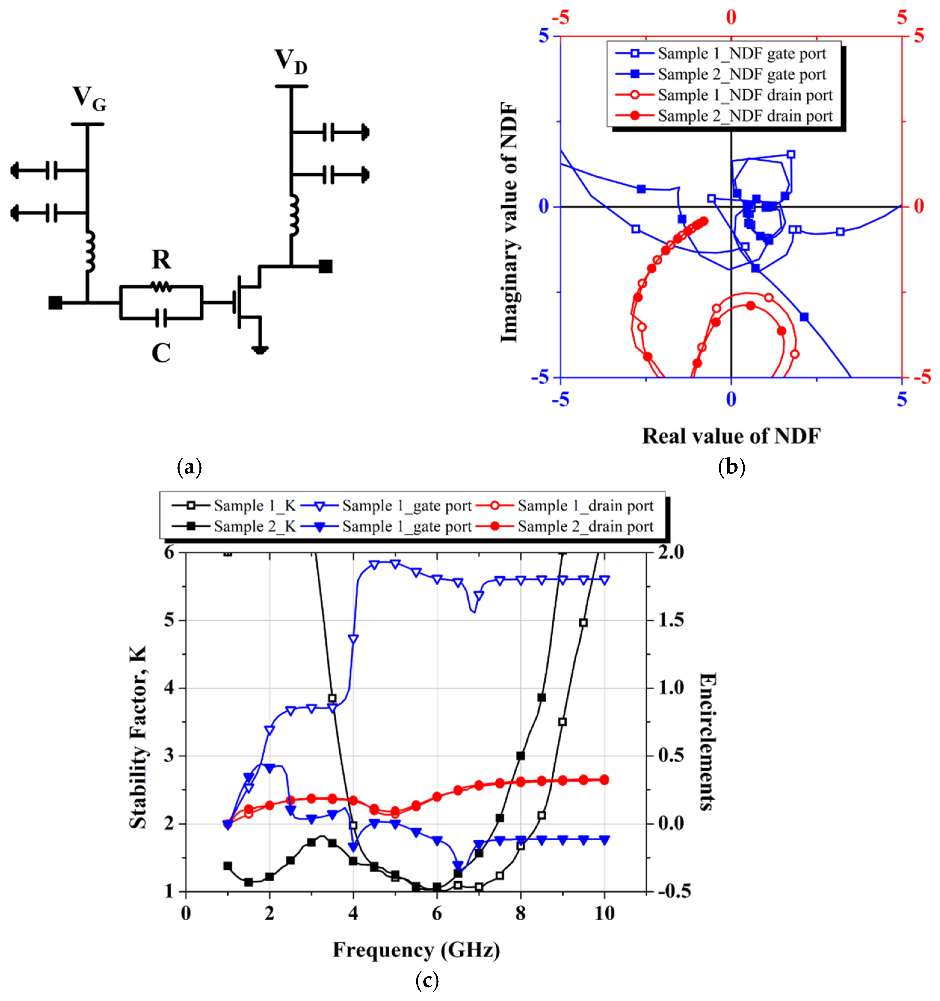
2.2. Network Determinant Function
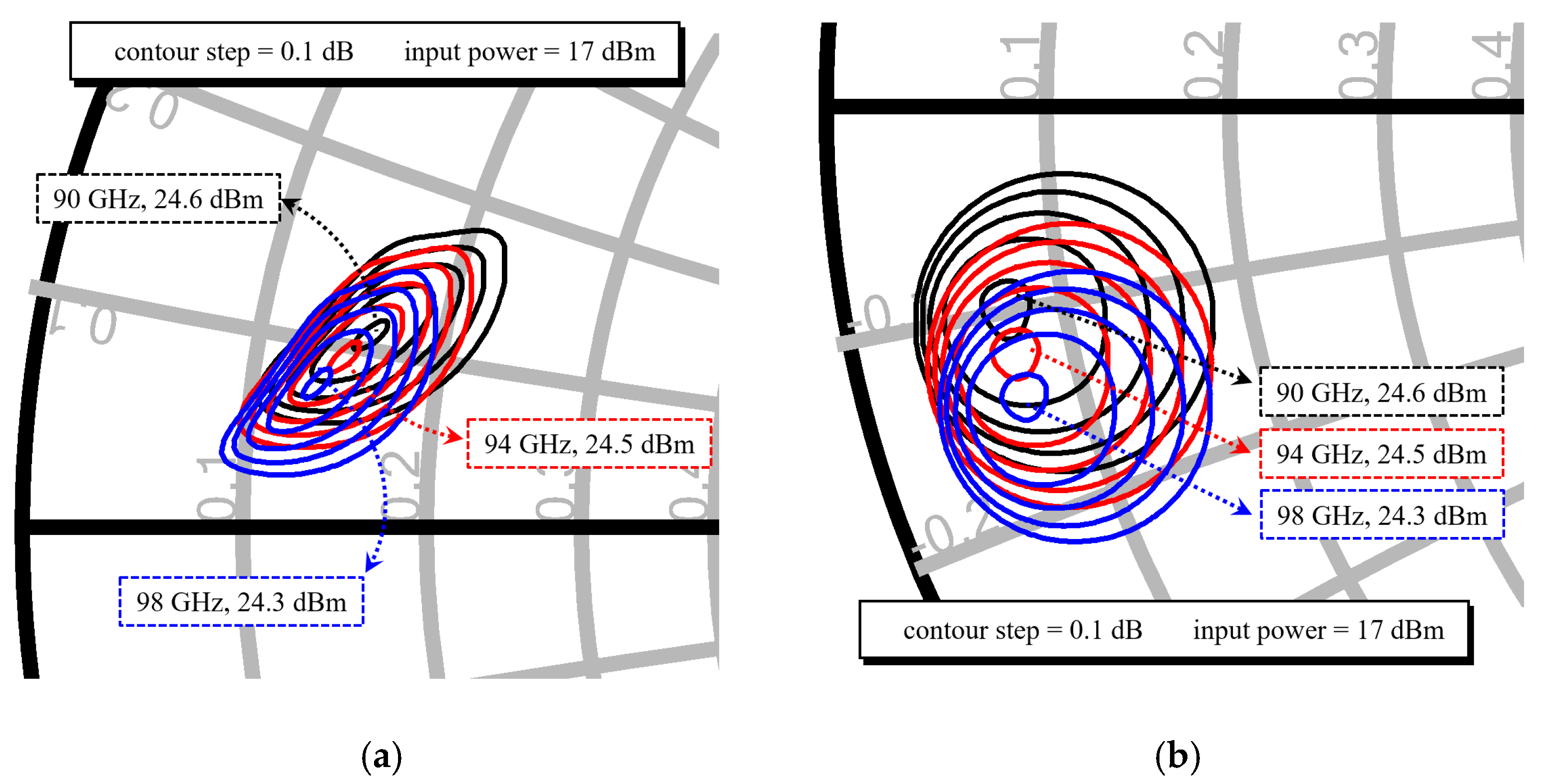
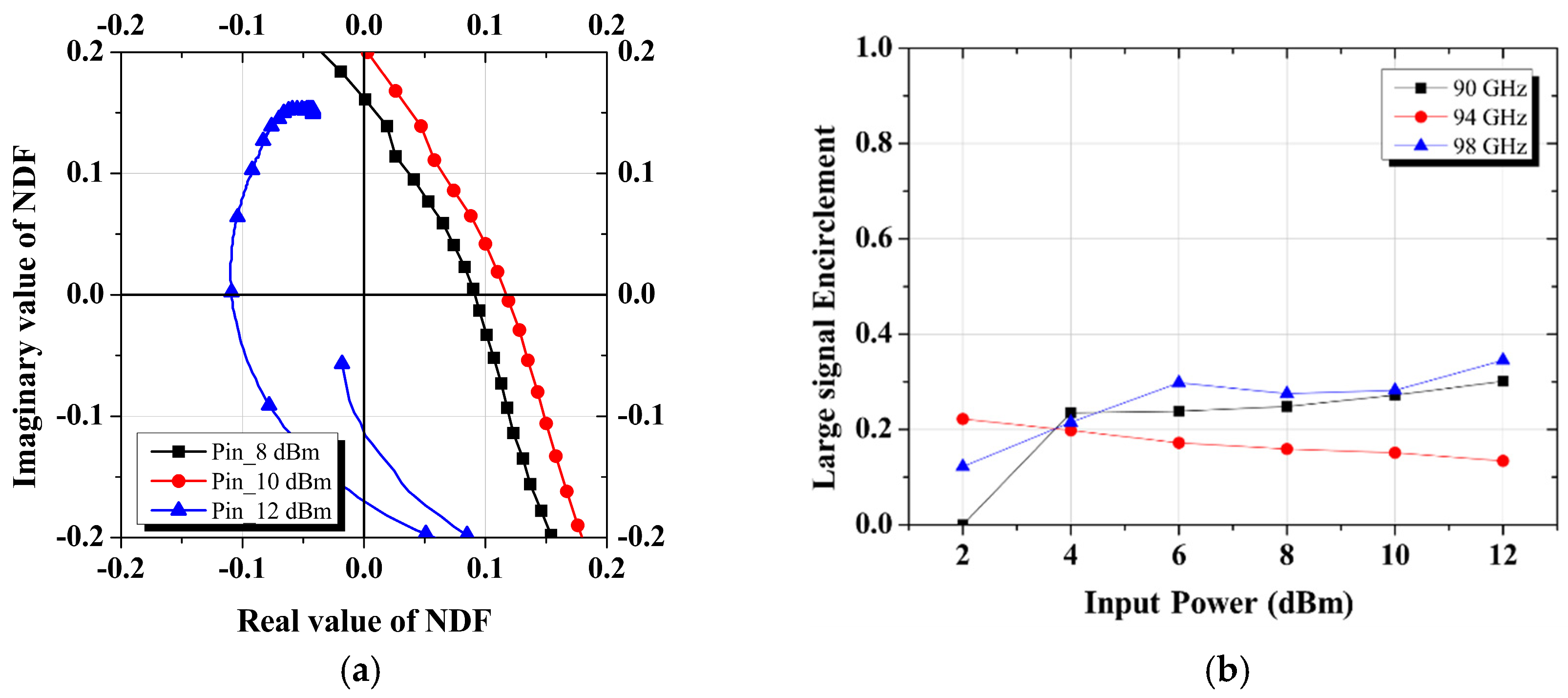
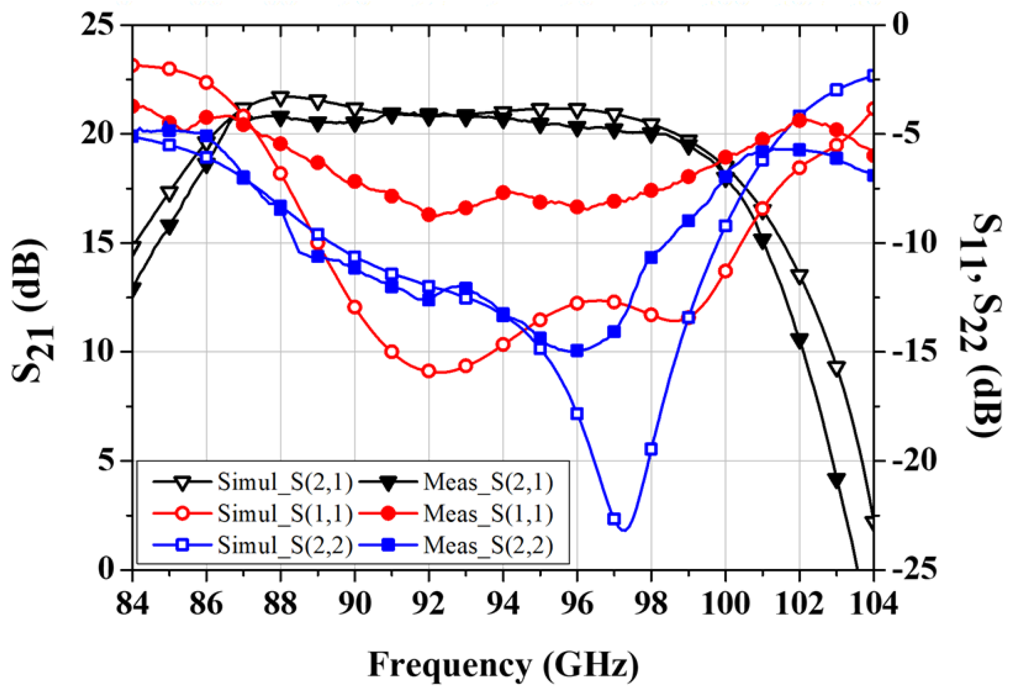
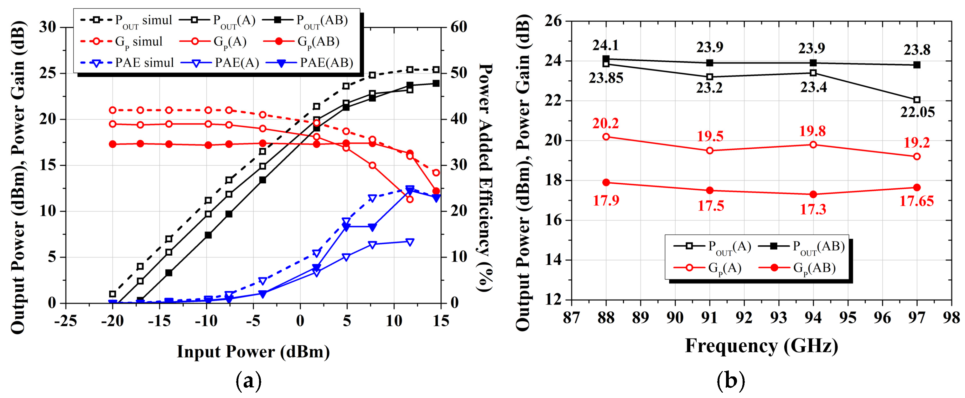
The K-factor is derived from the S parameters of a two-port circuit, as defined by Equations (1) and (2). Circuit stability is typically determined based on whether the K-value exceeds 1. However, it is important that even if the K-value is less than 1, the circuit may still operate stably under certain conditions [13].
For multi-stage circuits, relying only on the K-value as a stability criterion can lead to misleading conclusions, particularly due to the impact of matching losses between stages. In such cases, the normalized determinant function (NDF) provides a more robust approach to analyzing the circuit stability. The NDF evaluates both linear and nonlinear stability by applying a perturbation current to potentially unstable nodes, such as gate and drain nodes of transistors, and identifying oscillation frequencies using the determinant function. This is especially effective for identifying and mitigating stability issues in complex multi-stage circuit design [14,15].
K = 1 S 11 2 S 22 2 + Δ 2 2 S 21 S 12
Δ = S 11 S 22 S 12 S 21
The NDF is derived using Equation (3), where |Y(ω)| represents the admittance matrix at the suspected node, and |Y₀(ω)| corresponds to the admittance matrix when all active elements in the circuit are passively transformed. In this context, passive operation of a transistor implies that its transconductance is non-positive, ensuring that the transistor cannot induce oscillation. The NDF for the entire circuit is determined by multiplying the individual NDF values calculated for each suspected node. Passive operation at the gate node is achieved when the gate is biased below the pinch-off voltage, while at the drain node, passive operation occurs when the drain bias voltage is set to 0 V [16].
N D F ω = Y ω Y 0 ω
E n c i c l e m e n t s = u n w r a p ( N D F ) u n w r a p ( N D F ω = 0 ) × ( 360 )
The NDF plot is presented in Figure 3, showing the results from test sample circuits used for comparison between the NDF and K-factor. Sample circuits 1 and 2 include the sub-circuit shown in Figure 3a, with the only difference being the resistor and capacitor values at the transistor gate. When the NDF is plotted as a function of frequency on a polar chart, if the curve encircles the origin more than once in a clockwise direction, the test circuit is identified as unstable [14], as demonstrated in Figure 3b.
Figure 3c numerically represents the number of times the NDF curve encircles the origin on the polar chart as the frequency increases, derived from Equation (4). According to this plot, both sample circuits satisfy K > 1 across the full band, but the NDF of the test sample circuit 1 encircles the origin more than once above 4 GHz, indicating instability. This emphasizes the importance of first performing an NDF check and adjusting the passive element values before estimating the stability using the K-factor.
In the development of the W-band power amplifier, the stability criterion described above was applied to avoid the potential oscillation issues. Figure 4 displays the NDF waveform for the designed power amplifier, confirming stable operation as no RHP zeros are present across the entire frequency range.
Before assessing the oscillation (unstable condition) during nonlinear (or large-signal) operation, the circuit must first be unconditionally stable during linear (or small-signal) operation. In other words, nonlinear NDF calculations are only performed after the circuit passes the linear NDF stability test. In this context, Y ω in Equation (3) represents the admittance matrix at the suspected node under large-signal input conditions, while Y 0 ω refers to the admittance matrix when the small-signal power is applied. By following this methodology, the circuit stability can be evaluated for each combination of the input power and frequency [17].
Figure 5 presents the results of applying the nonlinear NDF test to the designed W-band power amplifier MMIC shown in Figure 1. Figure 5a illustrates the NDF trajectories at 94 GHz with the input power. Since the trajectory does not encircle the origin, it can be inferred that there are no RHP zeros, indicating that the circuit is stable. Additionally, the graph shown in Figure 5b depicts the large-signal encirclement as the input power and operating frequency change and shows that no large-signal encirclement exceeding 1 is observed during the nonlinear operation [14,17]. Therefore, it is concluded that the designed power amplifier remains stable during the nonlinear operation.

3. Measurement

Figure 6 shows the fabricated W-band power amplifier MMIC, which occupies an area of 1.0 × 2.6 mm2. The MMIC chip is mounted onto a CuW carrier using epoxy bonding. For the bias voltage supply, single-layer capacitors (SLCs) with the values of 10 nF and 100 pF are placed between DC pads on the chip and the evaluation PCB. The S-parameter measurements in the W-band are performed using an on-wafer probe system, a vector network analyzer (Keysight N5234B), WR-10 frequency extension modules (Keysight WR10-VNAX), and mm-wave test controllers (Keysight N5295A).
To measure the large-signal performance in the W-band, Ku-band signals are up-converted to W-band signals using a 6× frequency multiplier. The output of the multiplier is transferred to a W-band driving amplifier and a W-band attenuator to control the input power. The measurement setup includes a signal generator (Keysight E8257D), a 6× multiplier (Millitech AMC-10-RNHB3), power sensors (Anritsu MA24510A), and a driving amplifier (Eravant SBP-9039832526-1010-E1).
Figure 7 shows the measured S-parameter results of the power amplifier MMIC under the bias conditions of VDS = 4 V and IDQ = 360 mA. The input return loss exceeds 6 dB in the 88–98 GHz frequency range, and the gain is greater than 20 dB. The gain is decreased by about 1 dB, and input return loss is degraded by about 5 dB, partly due to some mismatch in the W-band between the transistor model and the transistor’s measured data, while the measured output return loss is in good agreement with the simulation data.
Figure 8a presents large signal characteristics of the fabricated W-band power amplifier MMIC at 94 GHz. The measurement under Class A bias conditions shows slight degradation in the output power compared to the simulated results. To enhance the output power, the bias conditions of the final stage were changed to a Class AB mode. As a result, the gain slightly decreased to 17.3–17.9 dB, but the output power increased by a maximum of 1.75 dB. Additionally, the maximum power-added efficiency (PAE) significantly improved from 13% to about 24%. Figure 8b shows the saturated output power and power gain as functions of frequency. Under Class-A bias conditions (gain mode), the output power was measured to range from 22.05 to 23.85 dBm, with a power gain of 19.2 to 20.2 dB. In contrast, under the Class-AB bias condition of the final stage (power mode), the output power increased to 23.8–24.1 dBm, while the power gain decreased to 17.3–17.9 dB within the 88–97 GHz frequency range.
Table 1 compares the results of this work with previously published W-band power amplifiers [18,19,20,21,22]. The fabricated W-band power amplifier MMIC in this work demonstrates comparable gain and output power performance to other published results while occupying a smaller area.

4. Conclusions

This study presents a compact and efficient W-band power amplifier MMIC using a 0.1 μm GaAs pHEMT process. To ensure both linear and nonlinear circuit stability, the normalized determinant function was employed under both small- and large-signal conditions across the frequency range from DC to 110 GHz. The developed amplifier achieves a linear gain of over 20 dB within the 88–98 GHz range. Under the large-signal operation, it delivers a saturated output power of 23.8–24.1 dBm with a power gain of 17.3–17.9 dB in a continuous wave mode. When the final amplification stage operates in a Class A bias mode, the power amplifier demonstrates an output power of 22.1–23.9 dBm with a power gain of 19.2–20.2 dB. With the final stage operating in a Class AB mode, the output power increases by a maximum of 1.75 dB, and the PAE improves by 11%, with a maximum gain reduction of 2.5 dB.
The W-band power amplifier developed in this study offers high output power while maintaining a compact size, making it suitable for a wide range of applications, including high-resolution radar systems and proximity fuses for both military and civilian purposes.

Author Contributions

Conceptualization and design, S.-H.H. and D.-W.K.; measurement, S.-H.H.; writing, S.-H.H. and D.-W.K.; supervision and project administration, D.-W.K. All authors have read and agreed to the published version of the manuscript.

Funding

This work was financially supported by Wavepia, Republic of Korea.

Data Availability Statement

Data are contained within this article.

Conflicts of Interest

The authors declare no conflict of interest.

References

  1. Lee, B.H.; An, D.; Lee, M.K.; Lim, B.O.; Kim, S.D.; Rhee, J.K. Two-stage broadband high-gain W-band amplifier using 0.1-μm metamorphic HEMT technology. IEEE Elctron Device Lett. 2004, 25, 766–768. [Google Scholar] [CrossRef]
  2. Kim, B.; Tran, A.; Schellenberg, J. Full W-band power amplifier/combiner utilizing GaAs technology. In Proceedings of the 2012 IEEE/MTT-S International Microwave Symposium Digest, Montreal, QC, Canada, 17–22 June 2012. [Google Scholar]
  3. Hong, S.E.; Kim, I.E.; Bang, S.C. Trends of technology developments for mm-wave based 5G communications. Electron. Telecommun. Trends 2013, 28, 107–117. [Google Scholar]
  4. Jang, S.H.; Kong, S.W.; Lee, H.D.; Park, J.H.; Kim, K.S.; Lee, K.C. Millimeter and terahertz wave circuit and system technologies and trends for future mobile communications. Electron. Telecommun. Trends 2018, 33, 1–12. [Google Scholar]
  5. Kim, K.Y.; Kim, G.S.; Myung, J.H.; Yoon, C.H.; Shin, W.; Kim, C.S.; Moon, S.H.; Kim, K.P.; Kim, T. Research trends on limitless connections in wireless transmission and access technologies. Electron. Telecommun. Trends 2019, 34, 61–74. [Google Scholar]
  6. Barabi, A.; Ross, N.; Wolfman, A.; Shaham, O.; Socher, E. A +27 dBm psat 27 dB gain W-band power ampflier 0.1 μm GaAs. In Proceedings of the 2018 IEEE/MTT-S International Microwave Symposium, Philadelphia, PA, USA, 10–15 June 2018. [Google Scholar]
  7. Trew, R.J. Wide bandgap semiconductor transistors for microwave power amplifiers. IEEE Microw. Mag. 2000, 1, 46–54. [Google Scholar] [CrossRef]
  8. Ge, Q.; Liu, W.; Xu, B.; Qian, F.; Yao, C. A 77–100 GHz power amplfier using 0.1-μm GaAs pHEMT technology. J. Semicond. 2017, 38, 035001. [Google Scholar] [CrossRef]
  9. Whelan, C.S.; Marsh, P.F.; Hoke, W.E.; McTaggart, R.A.; Lyman, P.S.; Leminias, P.J.; Lardizabal, S.M.; Leoni, R.E.; Lichwala, S.J.; Kazior, T.E. Millimeter-wave low noise and high power metamorphic HEMT amplifier on GaAs subtsrates. IEEE J. Solid State Circuits 2000, 35, 1307–1311. [Google Scholar] [CrossRef]
  10. Jung, K.K.; Yoon, J.S.; Chae, Y.S. Image measurement and processing using near-range passive millimeter-wave imaging system. J. Inst. Electron. Inf. Eng. 2015, 52, 1561–1567. [Google Scholar]
  11. Lee, W.H.; Lee, W.J.; Chung, T.J. Trends of millimeter wave and terahertz imaging technologies. Electron. Telecommun. Trends 2012, 6, 114–123. [Google Scholar]
  12. Meng, Y.; Qing, A.; Lin, C.; Zang, J.; Zhao, Y.; Zhang, C. Passive millimeter wave imaging system based on helical scanning. Sci. Rep. 2018, 8, 7852. [Google Scholar] [CrossRef]
  13. Rollet, J. Stability and Power-Gain Invariants of Linear Two ports. IRE Trans. Circuit Theory 1962, 9, 29–32. [Google Scholar] [CrossRef]
  14. Platzker, A.; Struble, W. Rigorous determination of the stability of linear n-node circuits from network determinants and the appropriate role of the stability factor K of their reduced two-ports. In Proceedings of the Third International Workshop on Integrated Nonlinear Microwave and Millimeterwave Circuits, Duisburg, Germany, 5–7 October 1994. [Google Scholar]
  15. Platzker, A.; Struble, W.; Hetzler, K. Instabilities Diagnosis and the Role of K in Microwave Circuits. In Proceedings of the 1993 IEEE MTT-S International Microwave Symposium Digest, Atlanta, GA, USA, 14–18 June 1993. [Google Scholar]
  16. Struble, W.; Platzker, A. A rigorous yet simple method for determining stability of linear N-port networks. In Proceedings of the 15th Annual GaAs IC Symposium, San Jose, CA, USA, 10–13 October 1993. [Google Scholar]
  17. Barquinero, C.; Suarez, A.; Herrera, A.; Garcia, J.L. Complete Stability Analysis of Multifunction MMIC Circuits. IEEE Trans. Microw. Theory Tech. 2007, 55, 2024–2033. [Google Scholar] [CrossRef]
  18. Zhu, F.; Luo, G. A W-band balanced power amplifier in 0.1-μm GaAs pHEMT process. In Proceedings of the 2020 IEEE MTT-S International Wireless Symposium, Shanghai, China, 20–23 September 2018. [Google Scholar]
  19. Canales, F.D.; Abbasi, M. A 75–90 GHz high linearity MMIC power amplifier with integrated output power detector. In Proceedings of the 2013 IEEE MTT-S International Wireless Symposium, Seattle, WA, USA, 2–7 January 2013. [Google Scholar]
  20. Kim, B.; Tran, A.; Schellenberg, J. Full W-band power amplifier/combiner utilizing GaAs technology. In Proceedings of the 2013 IEEE MTT-S International Wireless Symposium, Beijing, China, 14–18 April 2013. [Google Scholar]
  21. Bessemoulin, A.; Rodriguez, M.; Tarazi, J.; McCulloch, G.; Parker, A.E.; Mahon, S.J. Compact W-band PA MMICs in commercially available 0.1-μm GaAs pHEMT process. In Proceedings of the 2015 IEEE Compound Semiconductor Integrated Circuit Symposium, New Orleans, LA, USA, 11–14 October 2015. [Google Scholar]
  22. Mihaljevic, J.; Chakraborty, S.; Mahon, S.J.; Heimlich, M. An 82–98 GHz medium power amplifier in a 0.1 μm GaAs pHEMT process. In Proceedings of the 2023 5th Australian Microwave Symposium, Melbourne, Australia, 16–17 February 2023. [Google Scholar]
Figure 1. Circuit schematic of the W-band power amplifier.
Micromachines 16 00081 g001
Figure 2. Simulated source pull and load pull results of the 4 × 50 μm transistor: (a) load pull; (b) source pull.
Micromachines 16 00081 g002
Figure 3. Stability check using K and NDF: (a) Test sample sub-circuit; (b) NDF graphs; (c) Encirclements (sample circuit 1: R = 50 Ω, C = 1 pF, sample circuit 2: R = 50 Ω, C = 6.8 pF).
Micromachines 16 00081 g003
Figure 4. NDF graphs of the designed W-band power amplifier MMIC: (a) polar chart; (b) encirclements.
Micromachines 16 00081 g004
Figure 5. NDF graphs of the designed W-band power amplifier MMIC during nonlinear operation: (a) polar chart at 94 GHz; (b) encirclements.
Micromachines 16 00081 g005
Figure 6. Photograph of the fabricated W-band power amplifier MMIC.
Micromachines 16 00081 g006
Figure 7. Measured S-parameter results of the W-band power amplifier MMIC.
Micromachines 16 00081 g007
Figure 8. Large-signal measurement results of the W-band power amplifier MMIC: (a) Output power performance with input power at 94 GHz; (b) Saturated output power and power gain in the 88–97 GHz region.
Micromachines 16 00081 g008
Table 1. Comparison of this work with previously published W-band power amplifier MMICs using the 0.1 μm GaAs process.
WorkFrequency (GHz)Linear Gain (dB)Output Power
(dBm)
DC Power
(mW)
PAE
(%)
Chip Size (mm2)
[18]84–1031521.51260N.A.2 mm2
[19]75–84252050010.5 *2.1 mm2
[20]75–11016.515.53559.65 mm2
[21]80–1001224.5350N.A.3.5 mm2
[22]80–98≥202015813.33.72 mm2
This
work
88–97≥2022.1–23.9 (gain mode)1440132.6 mm2
23.8–24.1 (power mode)101024
*: estimated value.
Disclaimer/Publisher’s Note: The statements, opinions and data contained in all publications are solely those of the individual author(s) and contributor(s) and not of MDPI and/or the editor(s). MDPI and/or the editor(s) disclaim responsibility for any injury to people or property resulting from any ideas, methods, instructions or products referred to in the content.

