

Development of GaN-Based, 6.6 kW, 450 V, Bi-Directional On-Board Charger with Integrated 1 kW, 12 V Auxiliary DC-DC Converter with High Power Density


Abstract
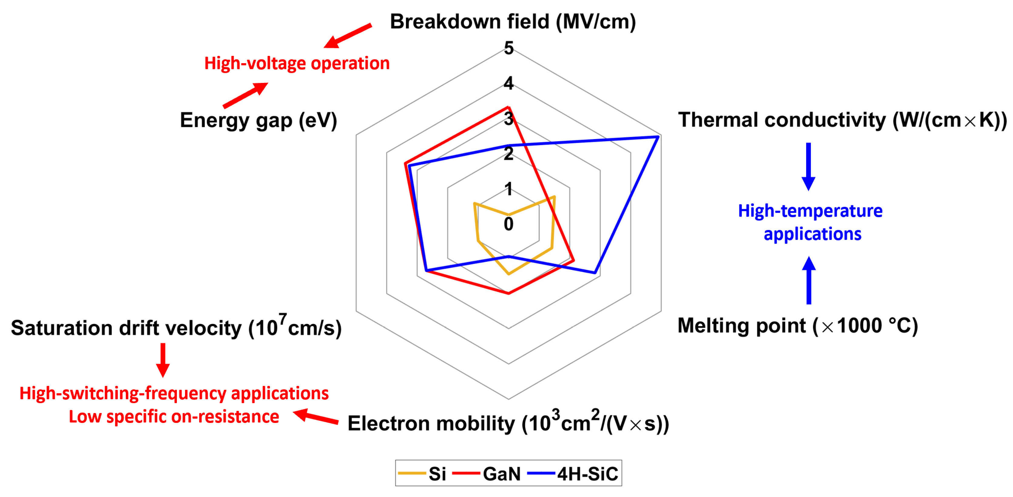
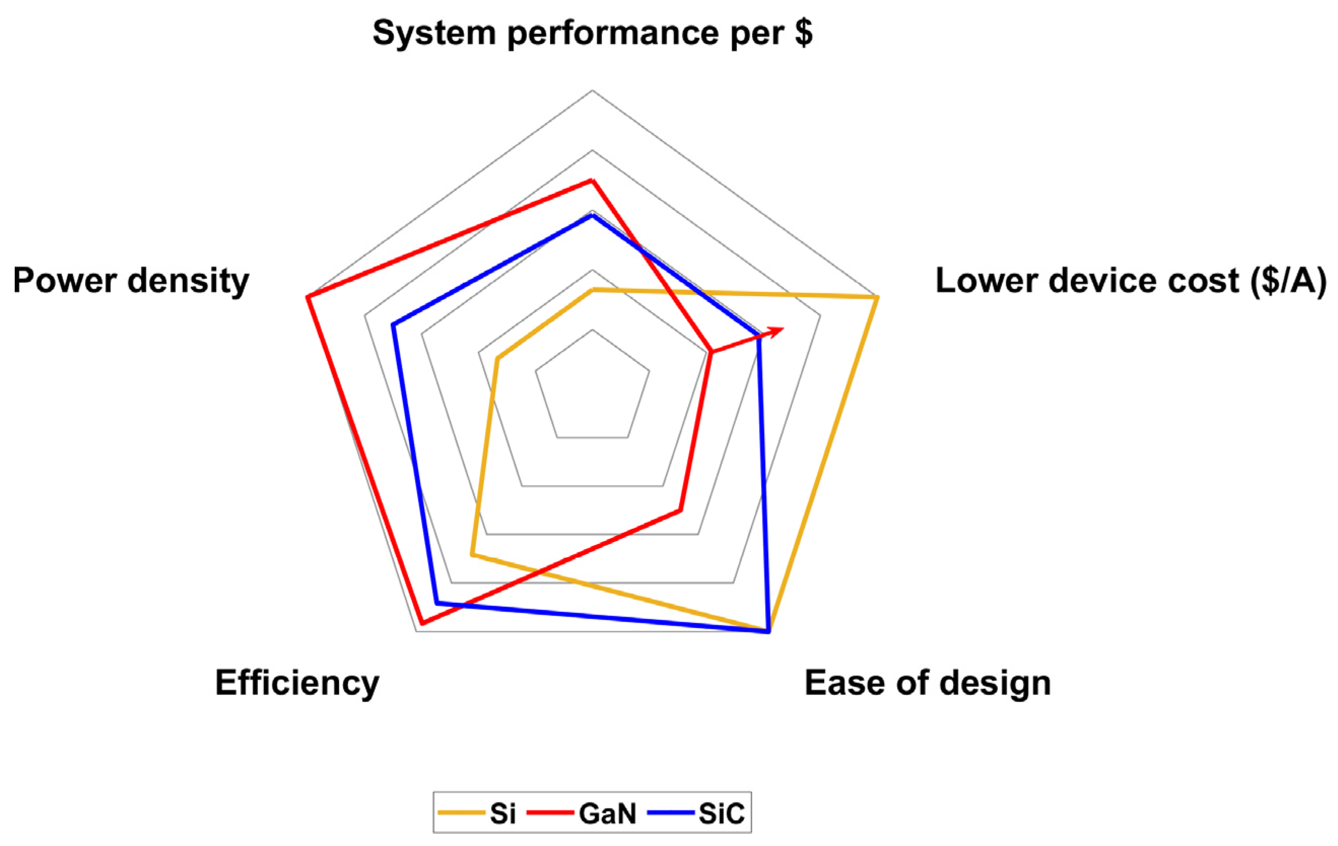
1. Introduction
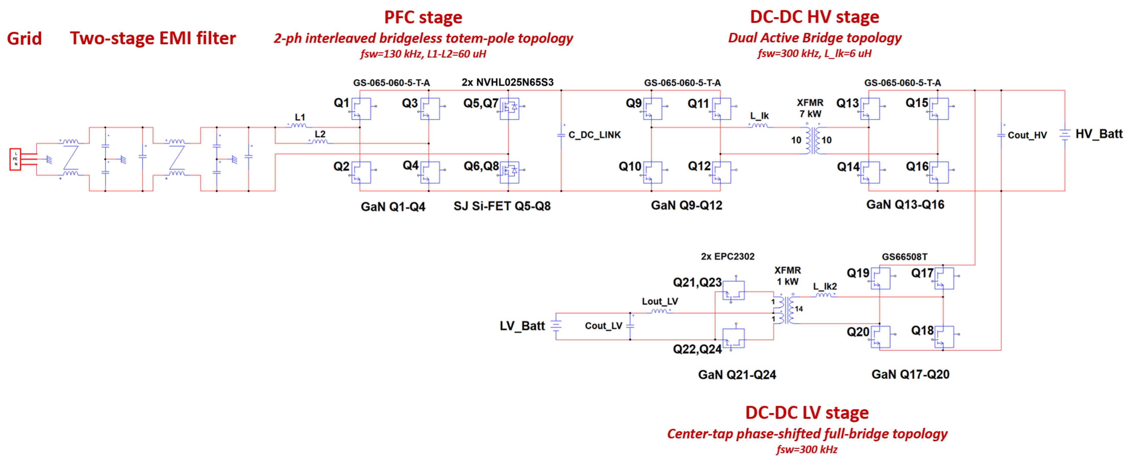
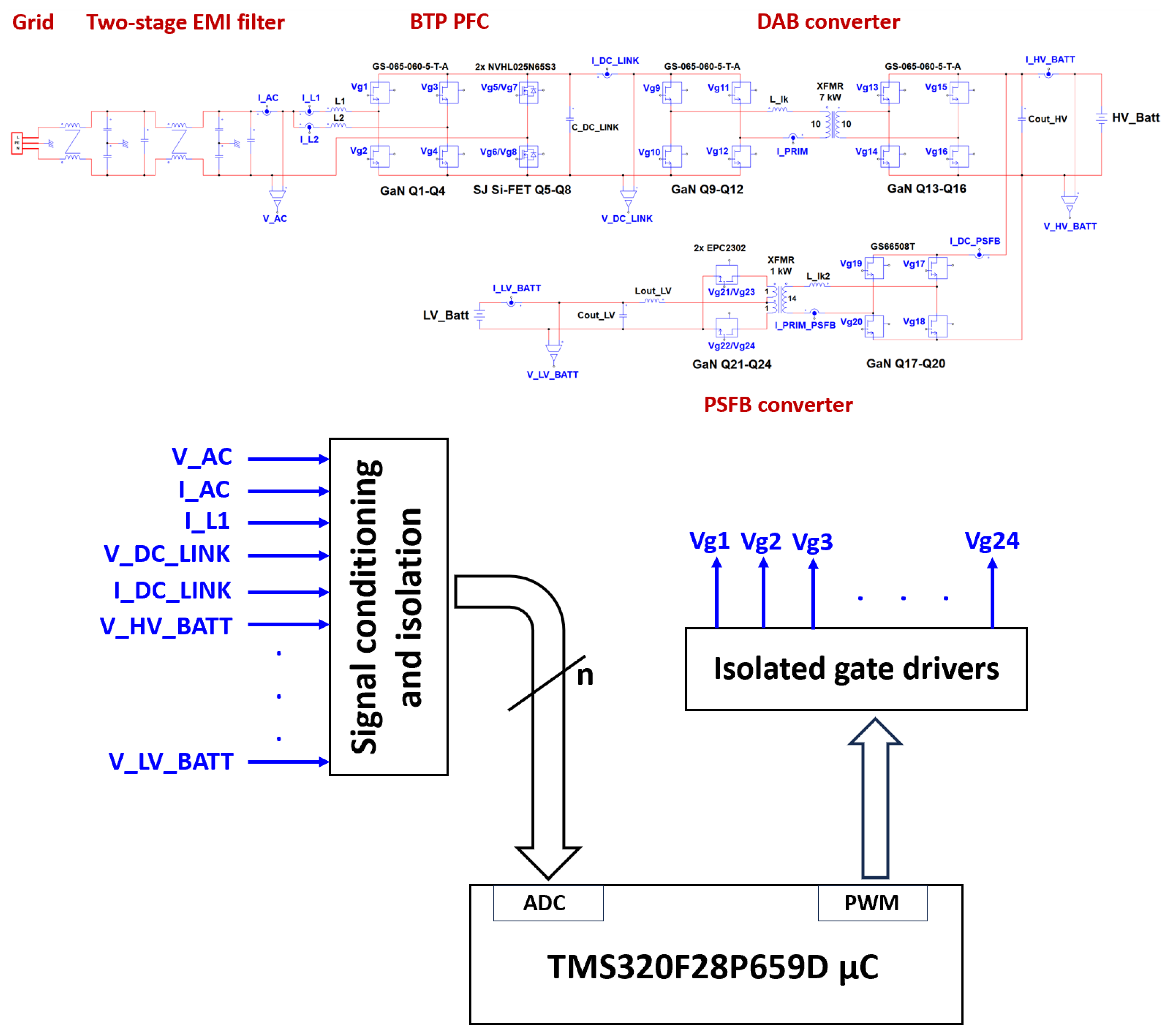
2. OBC Design
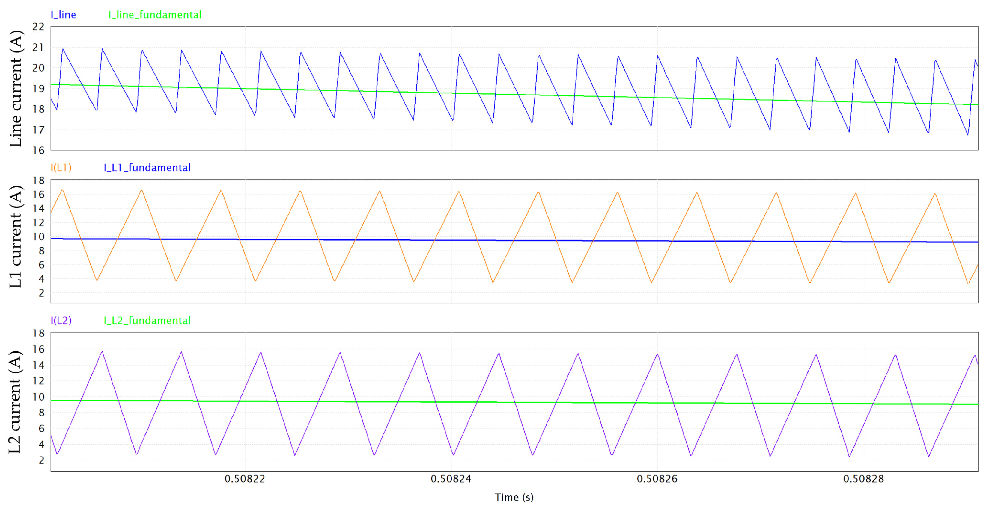
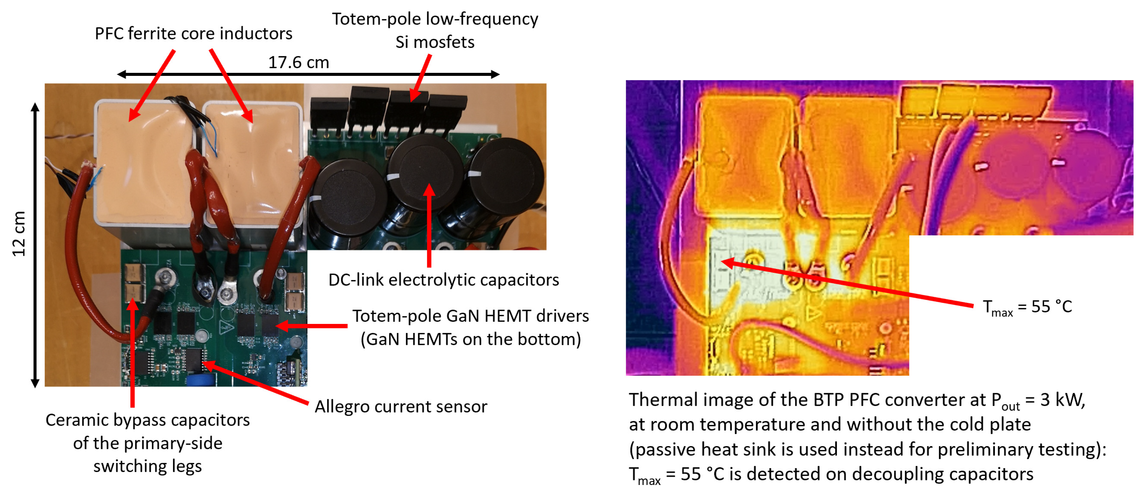
2.1. PFC Converter Design
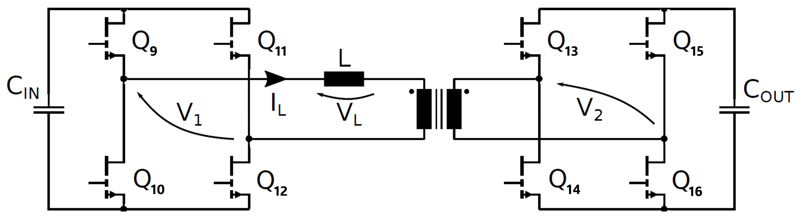
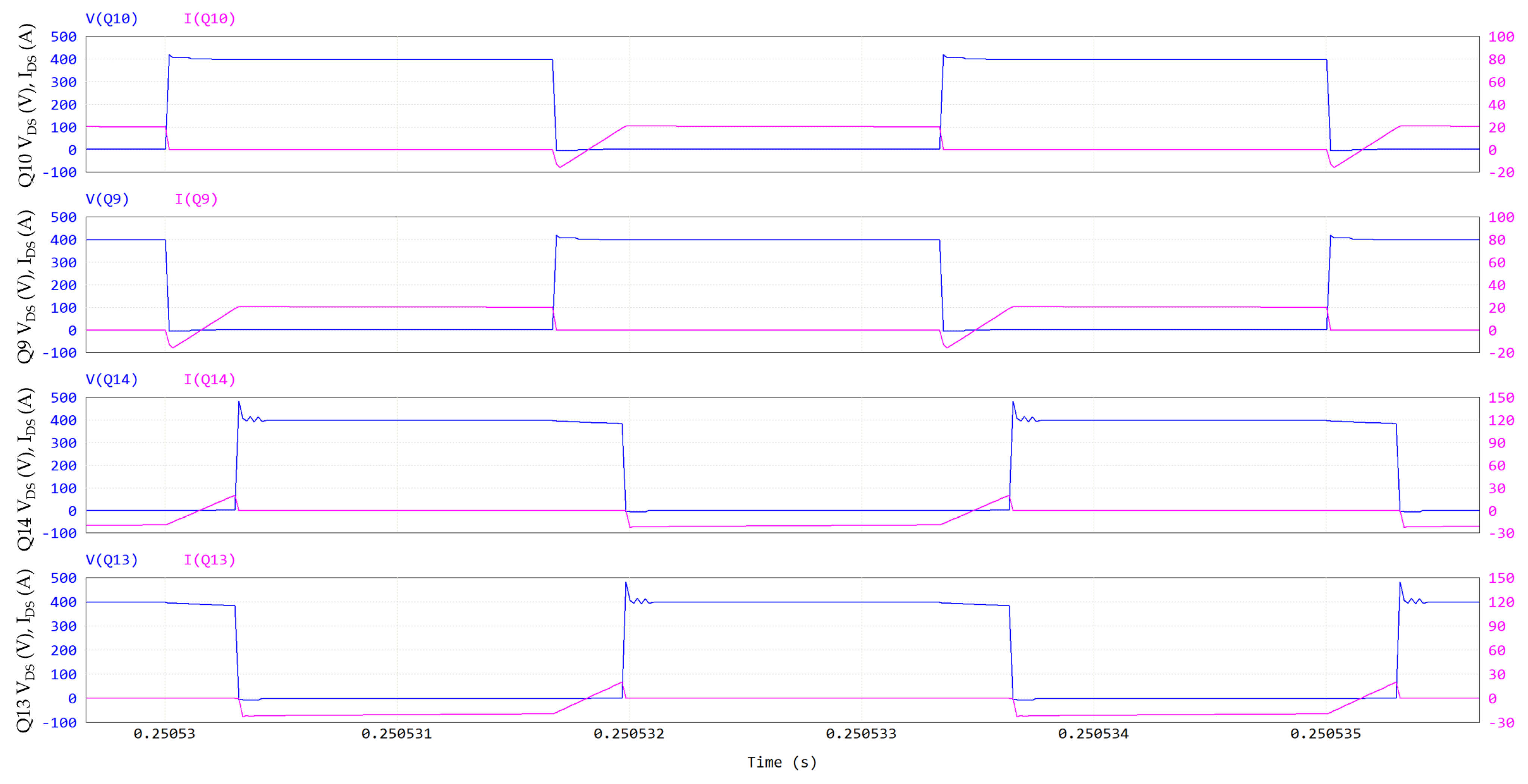
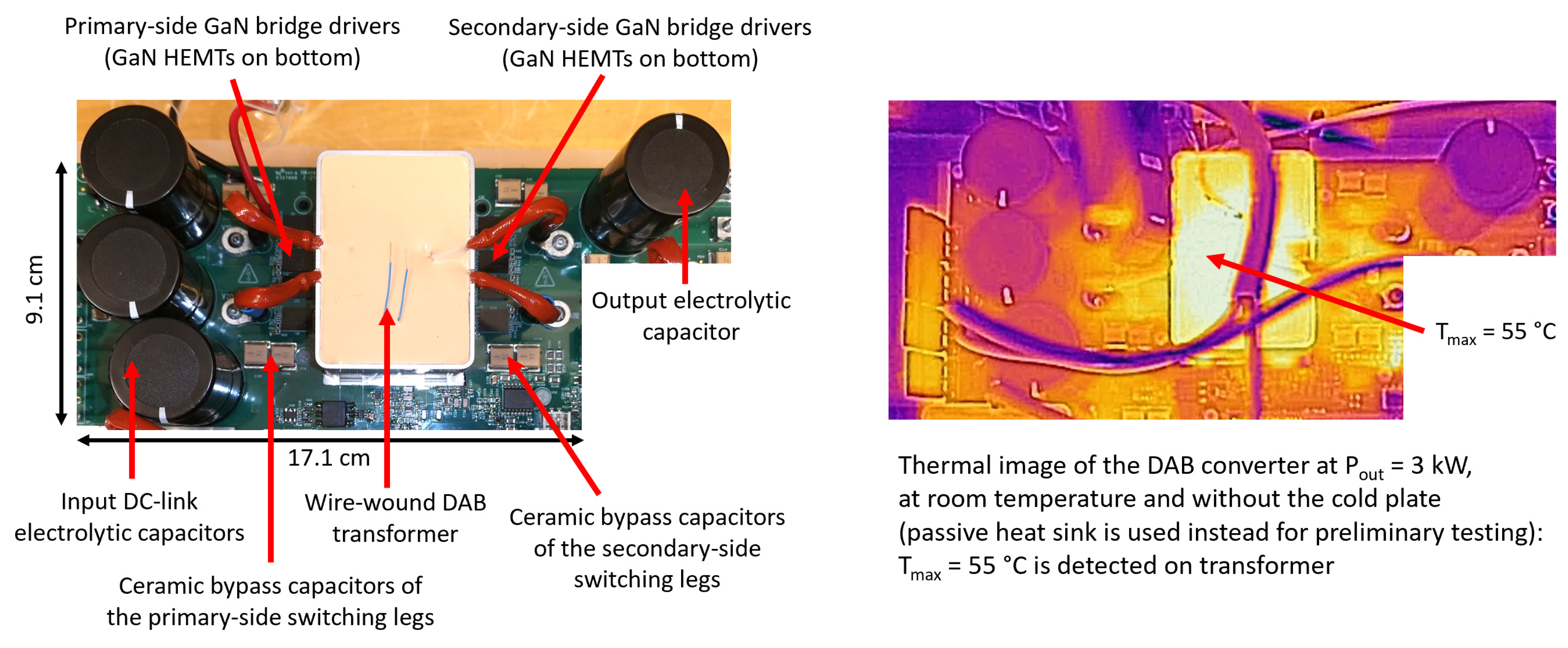
2.2. DAB Converter Design
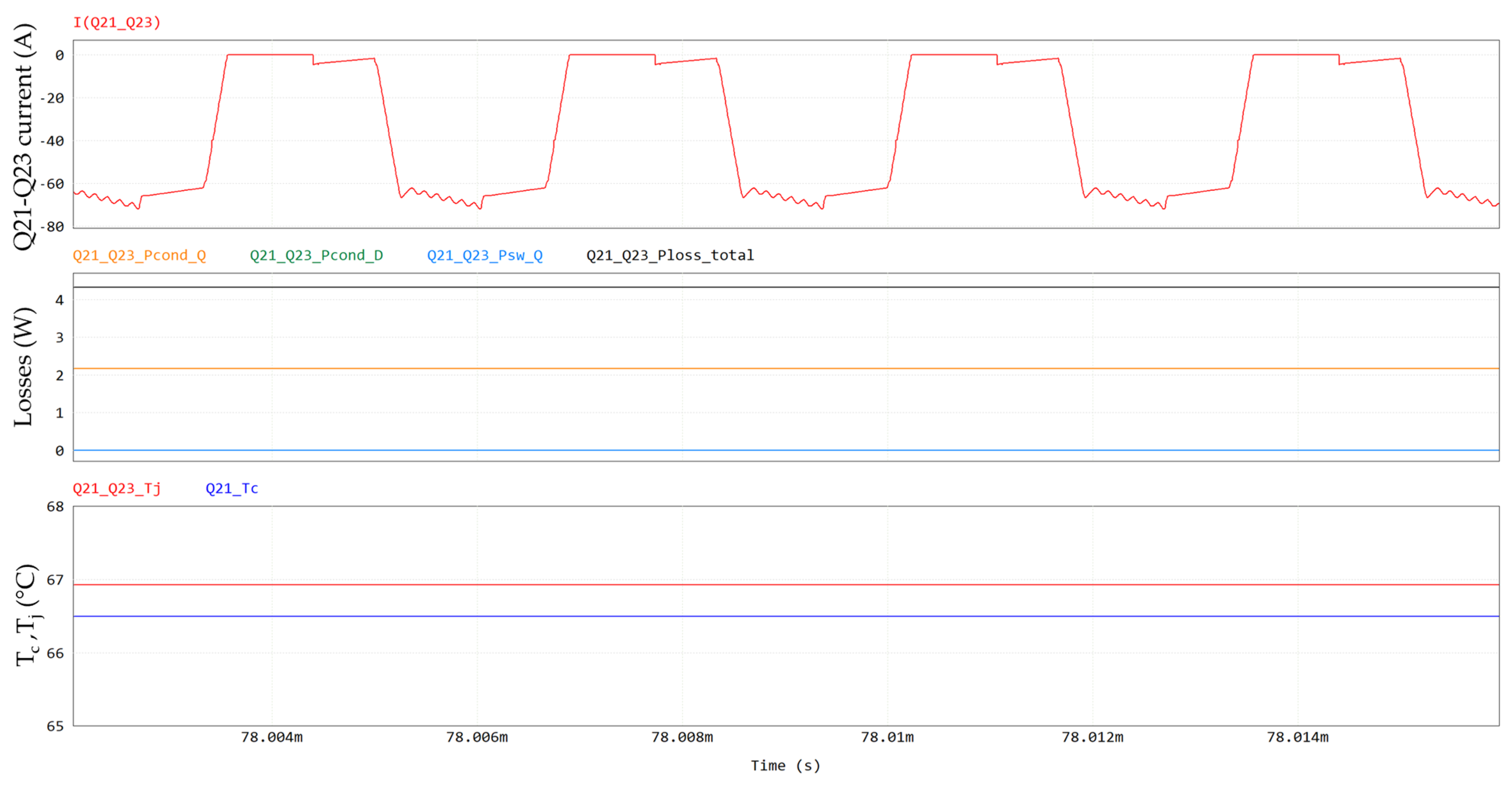
2.3. Auxiliary PSFB Converter Design
- The phase-shift full bridge (PSFB) with center-tapped synchronous rectification;
- The phase-shift full bridge with full-bridge synchronous rectification;
- The current-doubler phase-shift full bridge;
- The active-clamp forward with synchronous rectification;
- The resonant LLC.
2.4. Converter Control
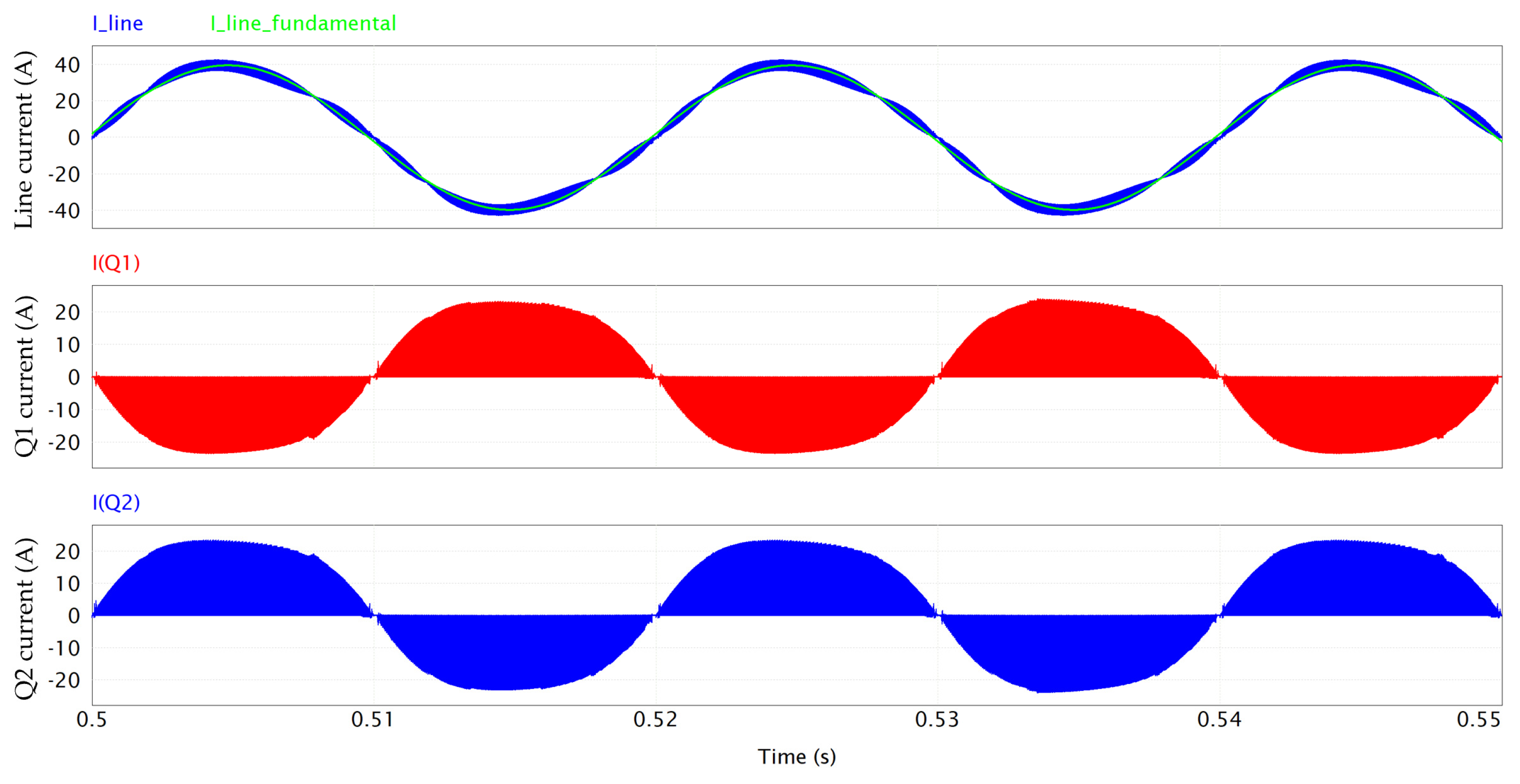
2.4.1. Bridgeless Totem-Pole PFC Control
- A PLL-SOGI filter is applied to the AC voltage-measured signal.
- An internal model compensator is applied to the input currents up to the ninth harmonic of the grid frequency.
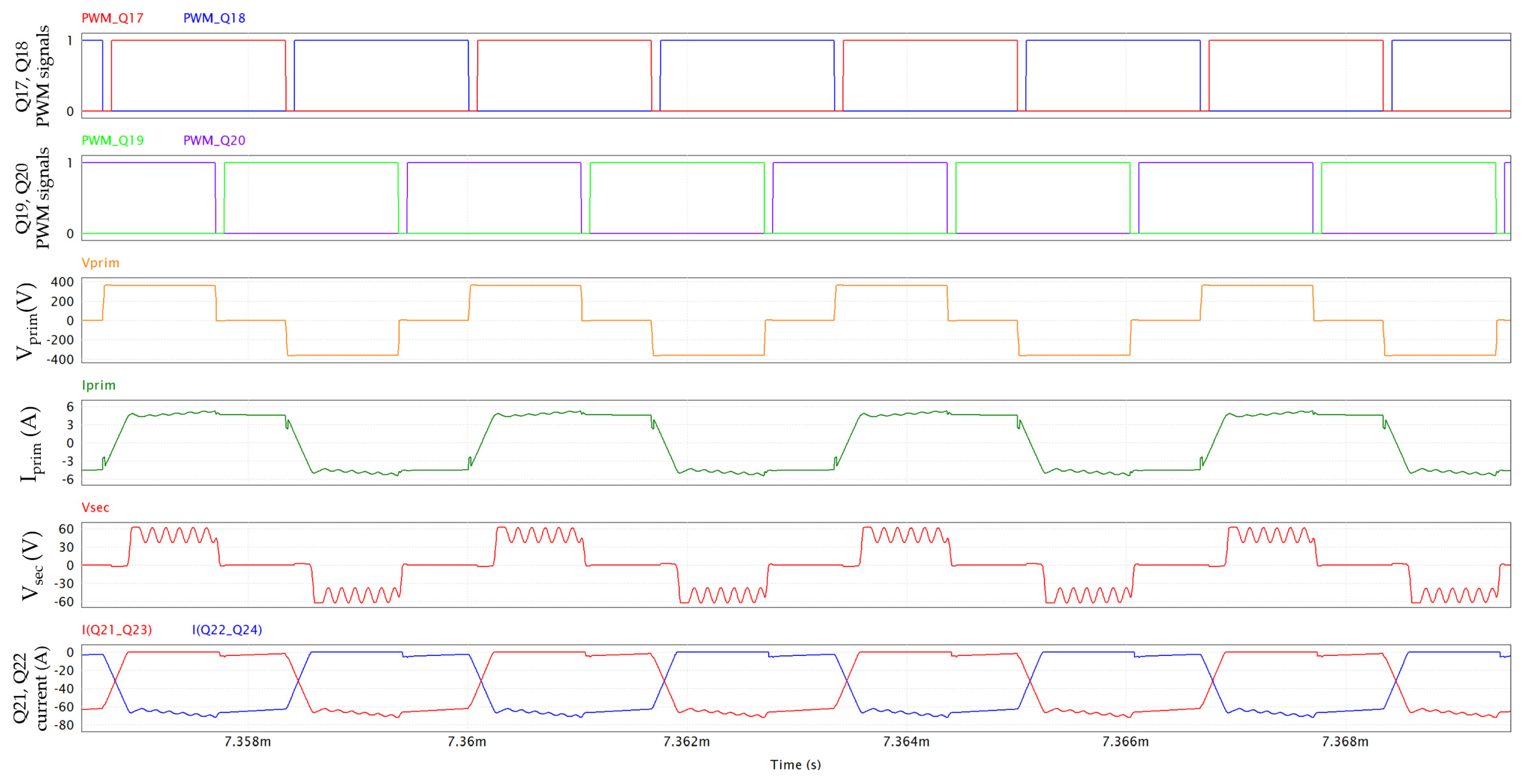
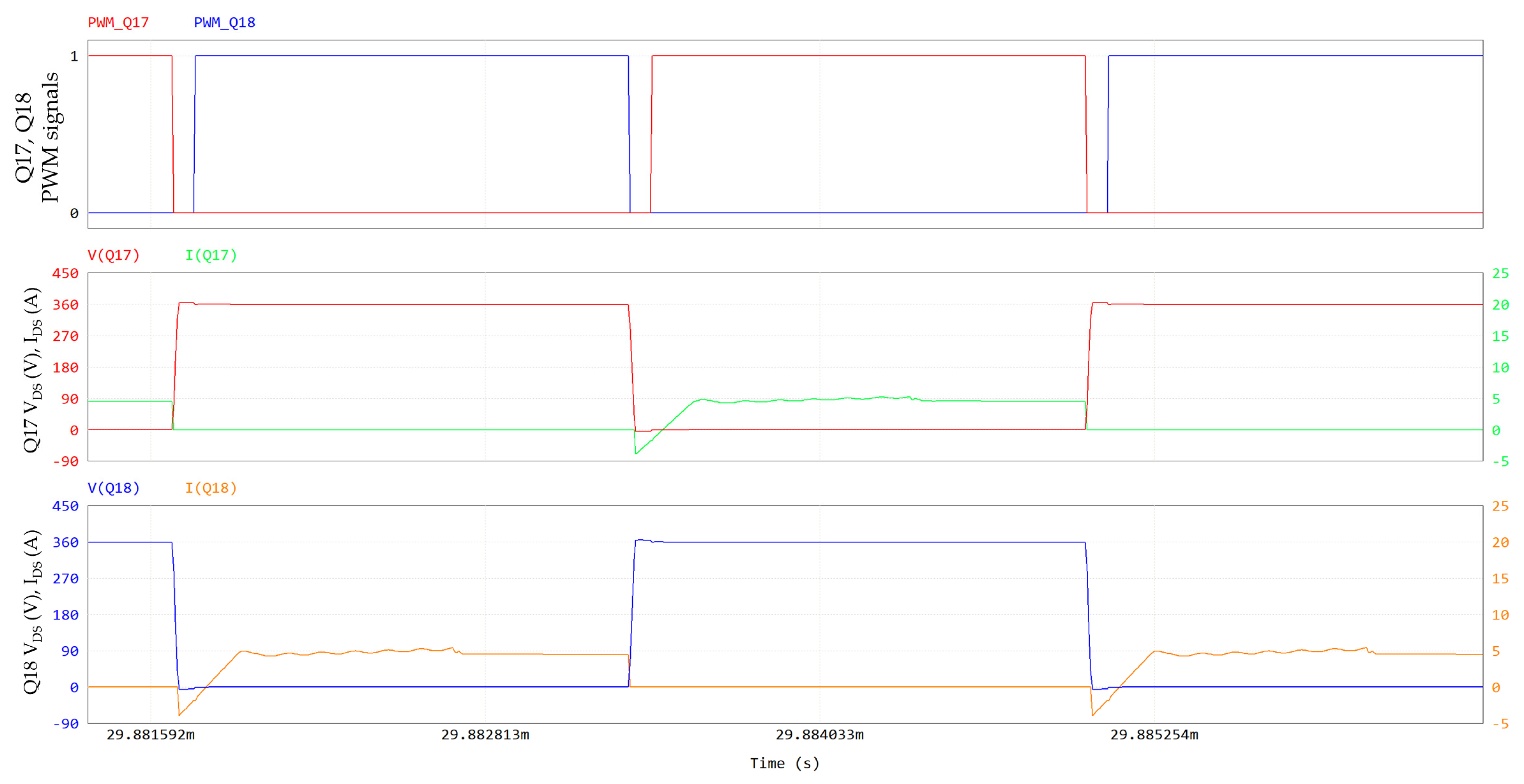
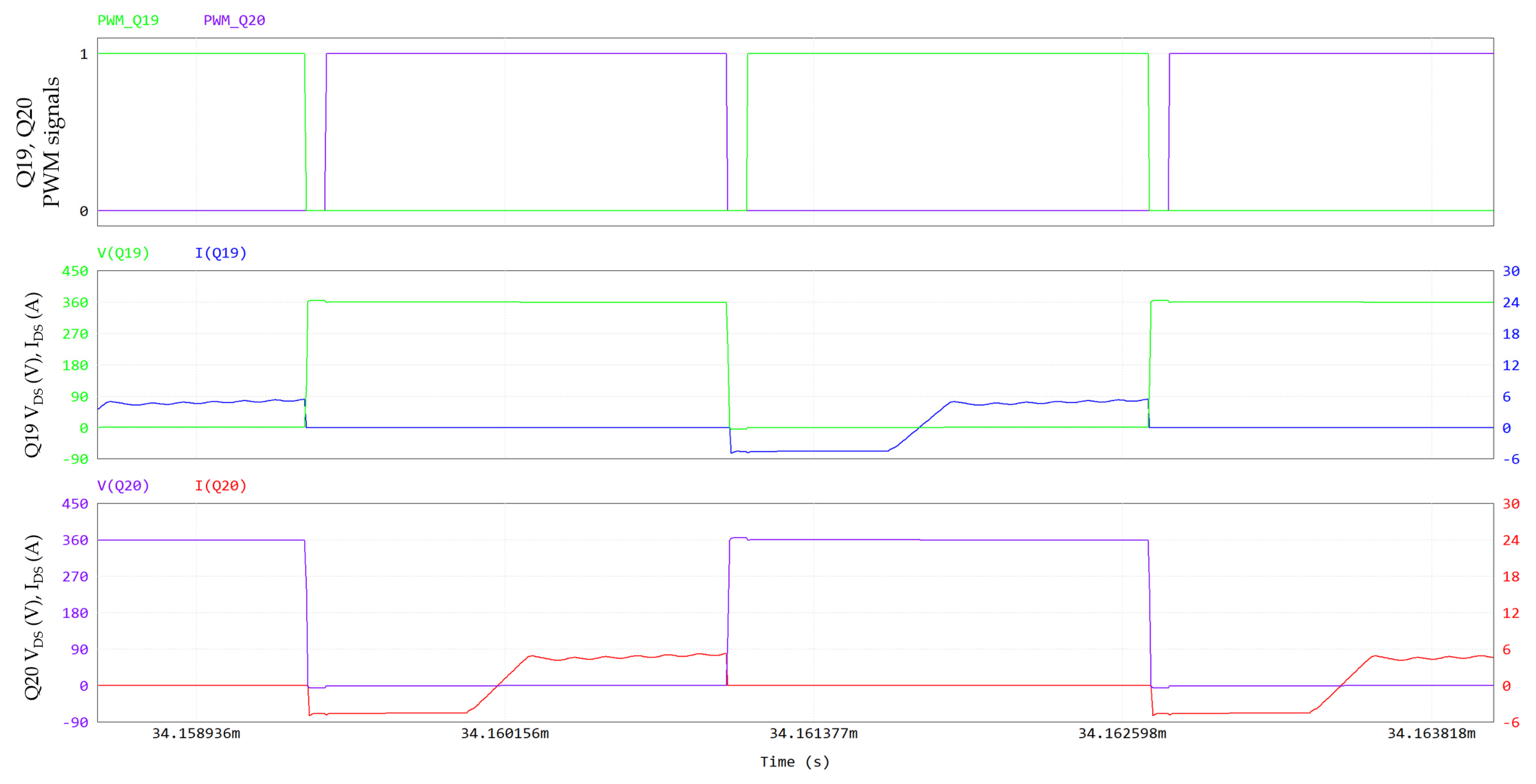
2.4.2. DAB Control
2.4.3. PSFB Control
2.4.4. Software
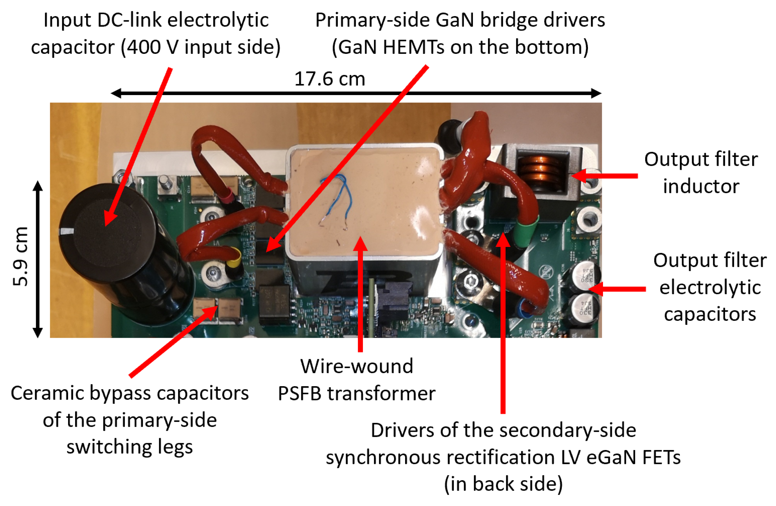
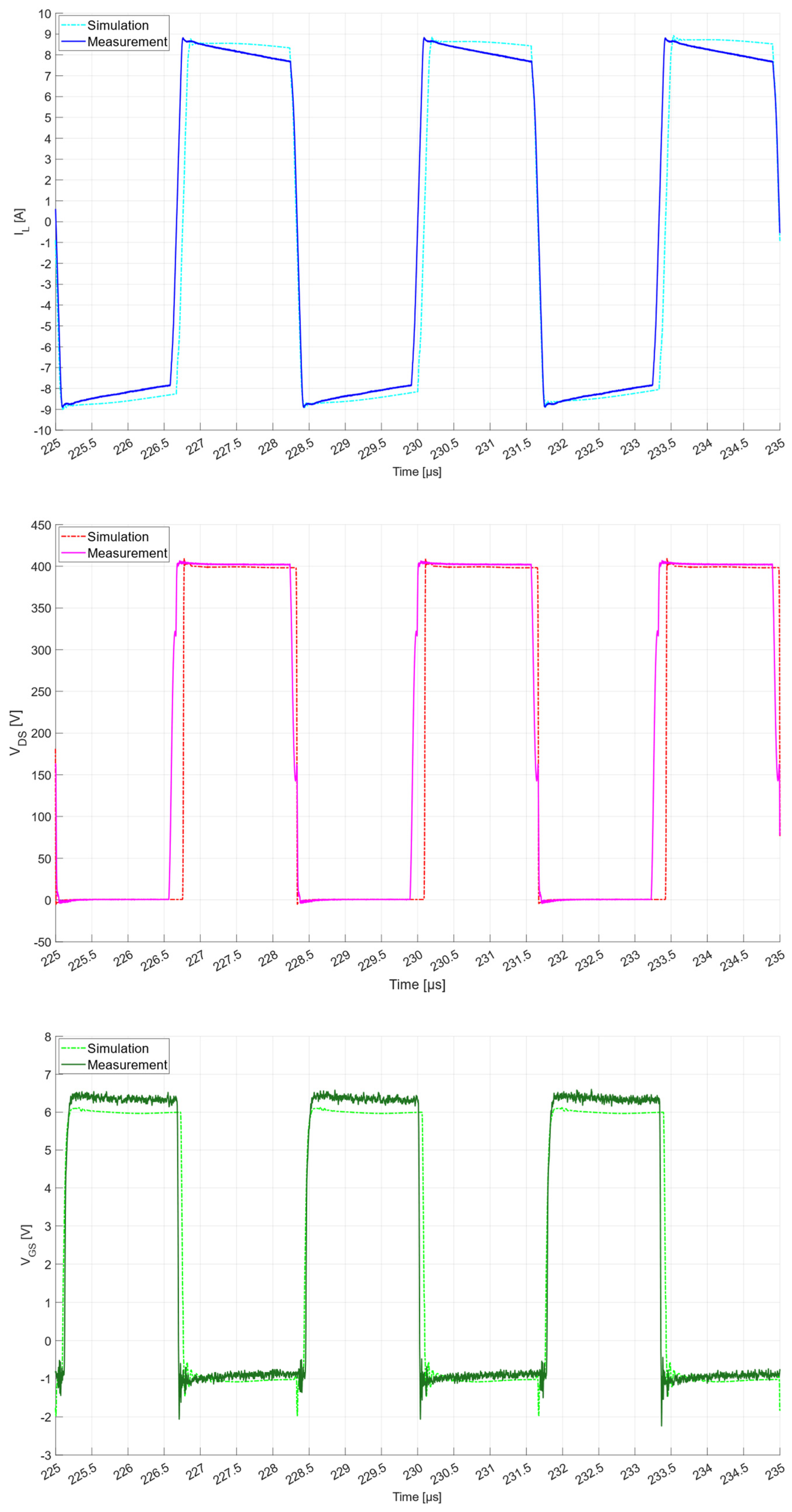
3. OBC Implementation and Validation Measurements
4. Conclusions
Author Contributions
Funding
Data Availability Statement
Conflicts of Interest
Abbreviations
| AC | alternating current |
| BEV | battery electric vehicle |
| BOM | bill of materials |
| BTP | bridgeless totem-pole |
| CAN | controller area network |
| CCM | continuous conduction mode |
| CMPSS | comparator subsystem |
| CrCM | critical conduction mode |
| DAB | dual active bridge |
| DC | direct current |
| DCM | discontinuous conduction mode |
| DCR | direct current resistance |
| EM | electromagnetic |
| ESL | equivalent series inductance |
| ESR | equivalent series resistance |
| EU | European Union |
| EV | electric vehicle |
| FET | field-effect transistor |
| GaN | gallium nitride |
| G2V | grid-to-vehicle |
| HEMT | high-electron-mobility transistor |
| HF | high-frequency |
| HV | high-voltage |
| IC | integrated circuit |
| LF | low-frequency |
| LV | low-voltage |
| L-N | line-neutral |
| OBC | on-board charger |
| PCB | printed circuit board |
| PCMC | peak-current mode control |
| PF | power factor |
| PFC | power factor correction |
| PI | proportional integral |
| PLL | phase-locked loop |
| PSFB | phase-shifted full-bridge |
| PWM | pulse width modulation |
| QFNL | quad flat no-lead |
| Si | silicon |
| SiC | silicon carbide |
| SOGI | second-order generalized integrator |
| SPS | single-phase-shift |
| THD | total harmonic distortion |
| TO | transistor outline |
| USA | United States of America |
| V2G | vehicle-to-grid |
| V2L | vehicle-to-load |
| WBG | wide-band-gap |
| XFMR | transformer |
| ZVS | zero-voltage switching |
| µC | microcontroller |
References
- Outlook for Electric Mobility. Available online: https://www.iea.org/reports/global-ev-outlook-2024/outlook-for-electric-mobility (accessed on 26 November 2024).
- Trends in Other Light-Duty Electric Vehicles. Available online: https://www.iea.org/reports/global-ev-outlook-2024/trends-in-other-light-duty-electric-vehicles (accessed on 26 November 2024).
- Trends in Heavy Electric Vehicles. Available online: https://www.iea.org/reports/global-ev-outlook-2024/trends-in-heavy-electric-vehicles (accessed on 26 November 2024).
- Grazian, F.; Soeiro, T.B.; Bauer, P. Voltage/Current Doubler Converter for an Efficient Wireless Charging of Electric Vehicles with 400-V and 800-V Battery Voltages. IEEE Trans. Ind. Electron. 2023, 70, 7891–7903. [Google Scholar] [CrossRef]
- Poorfakhraei, A.; Narimani, M.; Emadi, A. A Review of Multilevel Inverter Topologies in Electric Vehicles: Current Status and Future Trends. IEEE Open J. Power Electron. 2021, 2, 155–170. [Google Scholar] [CrossRef]
- Aghabali, I.; Bauman, J.; Kollmeyer, P.J.; Wang, Y.; Bilgin, B.; Emadi, A. 800-V Electric Vehicle Powertrains: Review and Analysis of Benefits, Challenges, and Future Trends. IEEE Trans. Transp. Electrif. 2021, 7, 927–948. [Google Scholar] [CrossRef]
- Parrino, G. How to Design a Traction Inverter with Infineon. In Proceedings of the Powering the Future: Wide Bandgap Technologies for Energy Efficiency in Industrial and Mobility, Arrow Event, Lazise, Italy, 22–24 January 2024. [Google Scholar]
- Morya, A.; Moosavi, M.; Gardner, M.C.; Toliyat, H.A. Applications of Wide Bandgap (WBG) Devices in AC Electric Drives: A Technology Status Review. In Proceedings of the 2017 IEEE International Electric Machines and Drives Conference (IEMDC), Miami, FL, USA, 21–24 May 2017; IEEE: Miami, FL, USA, 2017; pp. 1–8. [Google Scholar]
- Cimalla, V.; Pezoldt, J.; Ambacher, O. Group III Nitride and SiC Based MEMS and NEMS: Materials Properties, Technology and Applications. J. Phys. D Appl. Phys. 2007, 40, S19. [Google Scholar] [CrossRef]
- Emon, A.I.; Mustafeez-ul-Hassan; Mirza, A.B.; Kaplun, J.; Vala, S.S.; Luo, F. A Review of High-Speed GaN Power Modules: State of the Art, Challenges, and Solutions. IEEE J. Emerg. Sel. Top. Power Electron. 2023, 11, 2707–2729. [Google Scholar] [CrossRef]
- 7.4-kW EV or HEV Bidirectional Onboard Charger Reference Design with GaN; Design Guide TIDM-02013, TIDUF18 Rev. A; Texas Instruments: Dallas, TX, USA, 2024; Available online: https://www.ti.com/lit/ug/tiduf18a/tiduf18a.pdf (accessed on 26 November 2024).
- Jia, M.; Sun, H. GaN-Based High Frequency High Power Density 2-in-1 Bidirectional OBCM Design for EV Application. In Proceedings of the PCIM Europe 2023; International Exhibition and Conference for Power Electronics, Intelligent Motion, Renewable Energy and Energy Management, Nuremberg, Germany, 9–11 May 2023; pp. 1–10. [Google Scholar]
- Veliadis, V. Monolithic Bidirectional WBG Switches Rekindle Power Electronics Technology [Expert View]. IEEE Power Electron. Mag. 2023, 10, 71–75. [Google Scholar] [CrossRef]
- Weihe, S.; Menzi, D.; Huber, J.; Zhang, D.; Kolar, J.W.; Kasper, M.; Leong, K.K.; Deboy, G. Novel Bidirectional Single-Stage Isolated 600-V GaN M-BDS-Based Single/Three-Phase-Operable EV On-Board Charger. In Proceedings of the PCIM Europe 2024; International Exhibition and Conference for Power Electronics, Intelligent Motion, Renewable Energy and Energy Management, Nuremberg, Germany, 11–13 June 2024; pp. 330–337. [Google Scholar]
- Reusch, D.; Strydom, J. Understanding the Effect of PCB Layout on Circuit Performance in a High-Frequency Gallium-Nitride-Based Point of Load Converter. IEEE Trans. Power Electron. 2014, 29, 2008–2015. [Google Scholar] [CrossRef]
- Reali, A.; Alemanno, A.; Rossi, C.; Florian, C. Accurate Evaluation of Commutations of 650 V GaN Power Switches Assisted with EM Simulations in a 7 kW Dual Active Bridge Converter for Automotive Battery Charging Applications. Electronics, 2024; accepted. [Google Scholar]
- Sami, A.; Premoli, A. Electric Vehicle charging based on WBG. In Proceedings of the Powering the Future: Wide Bandgap Technologies for Energy Efficiency in Industrial and Mobility, Arrow Event, Lazise, Italy, 22–24 January 2024. [Google Scholar]
- Liu, Z.; Li, B.; Lee, F.C.; Li, Q. High-Efficiency High-Density Critical Mode Rectifier/Inverter for WBG-Device-Based On-Board Charger. IEEE Trans. Ind. Electron. 2017, 64, 9114–9123. [Google Scholar] [CrossRef]
- Liu, G.; Li, D.; Zhang, J.Q.; Jia, M.L. High Efficiency Wide Range Bidirectional DC/DC Converter for OBCM Application. In Proceedings of the 2014 International Power Electronics and Application Conference and Exposition, Shanghai, China, 5–8 November 2014; IEEE: Shanghai, China, 2014; pp. 1434–1438. [Google Scholar]
- Wei, C.; Zhu, D.; Xie, H.; Shao, J. A 6.6 kW High Power Density Bi-Directional EV on-Board Charger Based on SiC MOSFETs; Wolfspeed, Inc.: Durham, NC, USA, 2021; Available online: https://assets.wolfspeed.com/uploads/2021/04/bi-directional-ev-obc.pdf (accessed on 26 November 2024).
- High Efficiency CCM. Bridgeless Totem Pole PFC Design Using GaN E-HEMT; Reference Design GS665BTP-REF rev170905; GaN Systems: Richardson, TX, USA, 2018; Available online: https://gansystems.com/wp-content/uploads/2018/01/GS665BTP-REF-rev170905.pdf (accessed on 26 November 2024).
- Zhang, W.; Zhang, W.; Yang, J.; Al-Naemi, F. Comparisons between CRM and CCM PFC. Energy Power Eng. 2013, 5, 864–868. [Google Scholar] [CrossRef]
- POWERSIM Inc. PSIM User’s Manual, Version 2020a, 2020. Rev. 1. Available online: https://powersimtech.com/wp-content/uploads/2021/01/PSIM-User-Manual.pdf (accessed on 26 November 2024).
- GN001 Application Note: An Introduction to GaN Enhancement-Mode HEMTs, Rev. February 2018; GaN Systems: Richardson, TX, USA, 2018; Available online: https://gansystems.com/wp-content/uploads/2018/02/GN001_Design_with_GaN_EHEMT_180228-1.pdf (accessed on 26 November 2024).
- Gillmor, C. Predicting Output-Capacitor Ripple in a CCM Boost PFC Circuit; Technical Article SSZTB75; Texas Instruments: Dallas, TX, USA, 2016; Available online: https://www.ti.com/lit/ta/ssztb75/ssztb75.pdf (accessed on 26 November 2024).
- Gillmor, C. Analytic Expressions for Currents in the CCM PFC Stage; Texas Instruments: Dallas, TX, USA, 2018; Available online: https://www.ti.com/lit/ml/slyy131/slyy131.pdf (accessed on 26 November 2024).
- Yuan, J.; Dorn-Gomba, L.; Callegaro, A.D.; Reimers, J.; Emadi, A. A Review of Bidirectional on-Board Chargers for Electric Vehicles. IEEE Access 2021, 9, 51501–51518. [Google Scholar] [CrossRef]
- Lu, J.L.; Hou, R.; Chen, D. Opportunities and Design Considerations of GaN HEMTs in ZVS Applications. In Proceedings of the 2018 IEEE Applied Power Electronics Conference and Exposition (APEC), San Antonio, TX, USA, 4–8 March 2008; IEEE: San Antonio, TX, USA, 2018; pp. 880–885. [Google Scholar]
- He, P.; Khaligh, A. Comprehensive Analyses and Comparison of 1 kW Isolated DC–DC Converters for Bidirectional EV Charging Systems. IEEE Trans. Transp. Electrif. 2017, 3, 147–156. [Google Scholar] [CrossRef]
- Siebke, K.; Mallwitz, R. Comparison of a Dual Active Bridge and CLLC Converter for On-Board Vehicle Chargers Using GaN and Time Domain Modeling Method. In Proceedings of the 2020 IEEE Energy Conversion Congress and Exposition (ECCE), Detroit, MI, USA, 11–15 October 2020; IEEE: Detroit, MI, USA, 2020; pp. 1210–1216. [Google Scholar]
- Alemanno, A.; Morici, R.; Pretelli, M.; Florian, C. Design of a 7.5 kW Dual Active Bridge Converter in 650 V GaN Technology for Charging Applications. Electronics 2023, 12, 1280. [Google Scholar] [CrossRef]
- Lidow, A.; Rooij, M.; Strydom, J.; Reusch, D.; Glaser, J. GaN Transistors for Efficient Power Conversion, 1st ed.; Wiley: Hoboken, NJ, USA, 2019; pp. 132–135. [Google Scholar]
- Bahl, S.R.; Ruiz, D.; Lee, D.S. Product-Level Reliability of GaN Devices. In Proceedings of the 2016 IEEE International Reliability Physics Symposium (IRPS), Pasadena, CA, USA, 17–21 April 2016; IEEE: Pasadena, CA, USA, 2016; pp. 4A-3-1–4A-3-6. [Google Scholar]
- Alou, P.; Oliver, J.A.; Garcfa, O.; Prieto, R.; Cobos, J.A. Comparison of Current Doubler Rectifier and Center Tapped Rectifier for Low Voltage Applications. In Proceedings of the Twenty-First Annual IEEE Applied Power Electronics Conference and Exposition, 2006. APEC ’06, Dallas, TX, USA, 19–23 March 2006; IEEE: Dallas, TX, USA, 2006; pp. 744–750. [Google Scholar]
- Lu, J.; Khaligh, A. 1kW, 400V/12V High Step-down DC/DC Converter: Comparison between Phase-Shifted Full-Bridge and LLC Resonant Converters. In Proceedings of the 2017 IEEE Transportation Electrification Conference and Expo (ITEC), Chicago, IL, USA, 22–24 June 2017; IEEE: Chicago, IL, USA, 2017; pp. 275–280. [Google Scholar]
- Cetin, S.; Astepe, A. A Phase Shifted Full Bridge Converter Design for Electrical Vehicle Battery Charge Applications Based on Wide Output Voltage Range. In Proceedings of the 2016 International Conference on Applied Electronics (AE), Pilsen, Czech Republic, 6–7 September 2016; IEEE: Pilsen, Czech Republic, 2016; pp. 51–56. [Google Scholar]
- Rathore, A.K. Current-Fed DC/DC Converters for High Voltage Gain and Low Voltage High Current Applications: An Overview of Topologies and Modulation Techniques. In Proceedings of the 2016 IEEE International Conference on Power Electronics, Drives and Energy Systems (PEDES), Trivandrum, India, 14–17 December 2016; IEEE: Trivandrum, India, 2016; pp. 1–6. [Google Scholar]
- Xuewei, P.; Rathore, A.K. Naturally Clamped Zero-Current Commutated Soft-Switching Current-Fed Push–Pull DC/DC Converter: Analysis, Design, and Experimental Results. IEEE Trans. Power Electron. 2015, 30, 1318–1327. [Google Scholar] [CrossRef]
- O’Loughlin, M. 600-W, UCC28950/UCC28951 Phase-Shifted Full-Bridge; Application Note SLUA560D; Texas Instruments: Dallas, TX, USA, 2022; Available online: https://www.ti.com/lit/an/slua560d/slua560d.pdf (accessed on 26 November 2024).
- Yu, S.Y.; Lough, B.; Yin, L.C. Achieving High Converter Efficiency with an Active Clamp in a PSFB Converter; Texas Instruments: Dallas, TX, USA, 2023; Available online: https://www.ti.com/lit/an/slyt835/slyt835.pdf (accessed on 26 November 2024).
- Sun, B. How to Reduce Current Spikes at AC Zero-Crossing for Totem-Pole PFC; Texas Instruments: Dallas, TX, USA, 2015; Available online: https://www.ti.com/lit/an/slyt650/slyt650.pdf (accessed on 26 November 2024).
- Sun, B. Control Challenges in a Totem-Pole PFC; Texas Instruments: Dallas, TX, USA, 2017; Available online: https://www.ti.com/lit/an/slyt718/slyt718.pdf (accessed on 26 November 2024).
- Li, A. Optimized Control Schemes for Totem Pole PFC With Digital Controller; Application SPRADD9; Texas Instruments: Dallas, TX, USA, 2023; Available online: https://www.ti.com/lit/an/spradd9/spradd9.pdf (accessed on 26 November 2024).
- Alemanno, A.; Ronchi, F.; Rossi, C.; Pagliuca, J.; Fioravanti, M.; Florian, C. Design of a 350 kW DC/DC Converter in 1200-V SiC Module Technology for Automotive Component Testing. Energies 2023, 16, 2341. [Google Scholar] [CrossRef]
- Phase-Shifted Full Bridge DC/DC Power Converter Design Guide; Design Guide TIDU248; Texas Instruments: Dallas, TX, USA, 2014; Available online: https://www.ti.com/lit/ug/tidu248/tidu248.pdf (accessed on 26 November 2024).
- Peak Current Mode Controlled PSFB Converter Reference Design Using C2000™ Real-time MCU; Design Guide TIDM-02000, TIDUEO1 Rev. B; Texas Instruments: Dallas, TX, USA, 2021; Available online: https://www.ti.com/lit/ug/tidueo1b/tidueo1b.pdf (accessed on 26 November 2024).


| Manufacturer | PFC Topology | HV DC-DC Topology | Input Voltage (Vrms) | Output Voltage (V) | Nominal Power (kW) | Efficiency (%) | Power Density (kW/L) | Switching Devices |
|---|---|---|---|---|---|---|---|---|
| Texas Instruments [11] | 2-ph interleaved BTP | CLLC | 90–264 | 200–450 | 6.6 | 96.5 (@ 20 °C) | 3.8 (open frame) | GaN power ICs |
| Navitas Semiconductor 1 [12] | 2-ph interleaved BTP | CLLC | 85–265 | 250–500 | 6.6 | 96.24 (@ 45 °C) | 3.9 | GaN power ICs |
| Delta-Q [18,19] | 2-ph interleaved BTP | CLLC | 85–265 | 200–450 | 6.6 | 96 | 2.26 | GaN/SiC |
| Wolfspeed [20] | BTP | CLLC | 90–265 | 250–450 | 6.6 | 96.5 | 3.3 (open frame) | SiC |
| Proposed prototype 1 | 2-ph interleaved BTP | DAB | 90–264 | 200–450 | 6.6 | 96 (@ 60 °C) | 2.2 | GaN HEMTs |
| PFC Stage | DC-DC HV Stage | |||||||||
| AC Grid Range | Vout,nominal | Pout,nominal | Vin,nominal | Vout,range | Vout,nominal | Iout,nominal | Pout,nominal | Pout,max | ||
| 90–264 Vrms | 400 V | 6.6 kW | 400 V | 200–450 V | 400 V | 16.5 A | 6.6 kW | 7 kW | ||
| DC-DC LV Stage | Additional Requirements | |||||||||
| Vin,range | Vin,nominal | Vout,range | Vout,nominal | Pout,nominal | Pout,max | Bidirectional power flow CISPR 32/EN 55022/32 Class B compliance | ||||
| 240–450 V | 360 V | 10–16 V | 12 V | 800 W | 1 kW | |||||
| VDS | IDS (@ Tc = 25 °C) | IDS (@ Tc = 100 °C) | RDS,on (@ Tj = 25 °C) | RDS,on (@ Tj = 150 °C) | ||
| 650 V | 60 A | 41 A | 25 mΩ | 65 mΩ | ||
| Ciss (@ 400 V) | Coss (@ 400 V) | Cgd (@ 400 V) | Qgd (@ 400 V) | Qg (@ 400 V) | ||
| 516 pF | 127 pF | 2.4 pF | 4.1 nC | 14 nC | ||
| Eon, Eoff, Eoss (@ 400 V, 20 A, RG = 10/2 Ω, VGS = 6/−3 V, Tj = 25 °C) | ||||||
| 117 µJ | 17.2 µJ | 17 µJ | ||||
| Package inductances Lg, Ld, Ls (from Pspice level 3 model) | ||||||
| 4 nH | 0.2 nH | 0.3 nH | ||||
| Passive Component | PN | Quantity | Parameters |
|---|---|---|---|
| PFC inductor | Bourns custom design | 2× | L = 60 µH (@ 1 V, 100 kHz) RDC = 22 mΩ Saturation Current: 20% Roll off |
| 3× | VDC = 500 V C = 390 µF | ||
| Electrolytic capacitor | Kemet ALA7DA391CF500 | ESR = 481.2 mΩ (@ 20 °C, 10 kHz) ESL = 20 nH Icrms = 4.12 Arms (@ 85 °C, 10 kHz) | |
| VDC = 500 V C = 1 µF | |||
| Ceramic capacitor | TDK B58031U5105M062 | 2× for each GaN leg | ESR = 12 mΩ (@ 0 VDC, 0.5 Vrms, 25 °C, 1 MHz) ESL = 3 nH Icrms = 11 Arms (@ 85 °C, 100 kHz) |
| Quantity | RMS Value | Mean Value |
|---|---|---|
| Vout | 400.37 Vrms | 400.06 V |
| Iout | 16.52 Arms | 16.50 A |
| IC,DC-link | 13.32 Arms | ≈0 A |
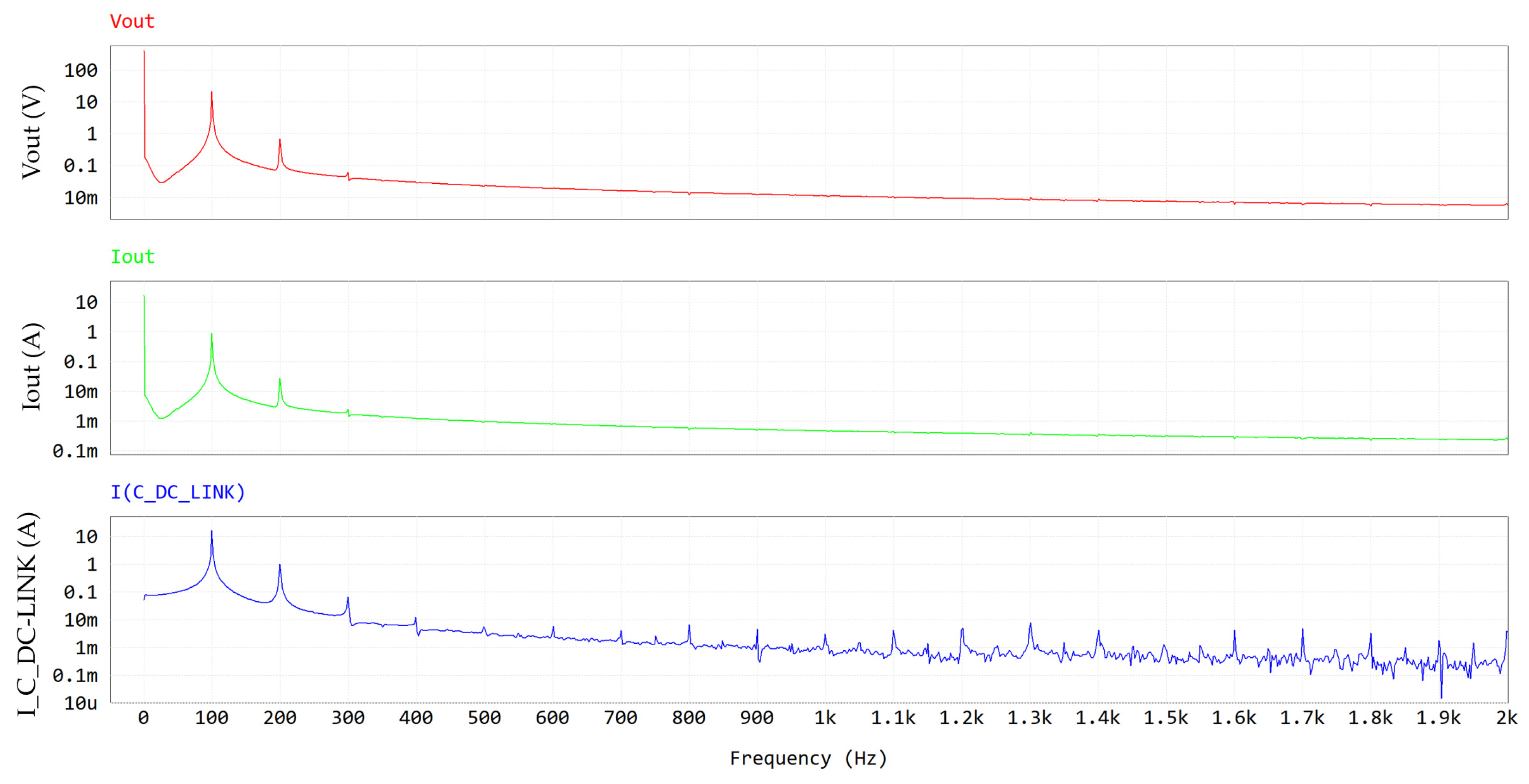
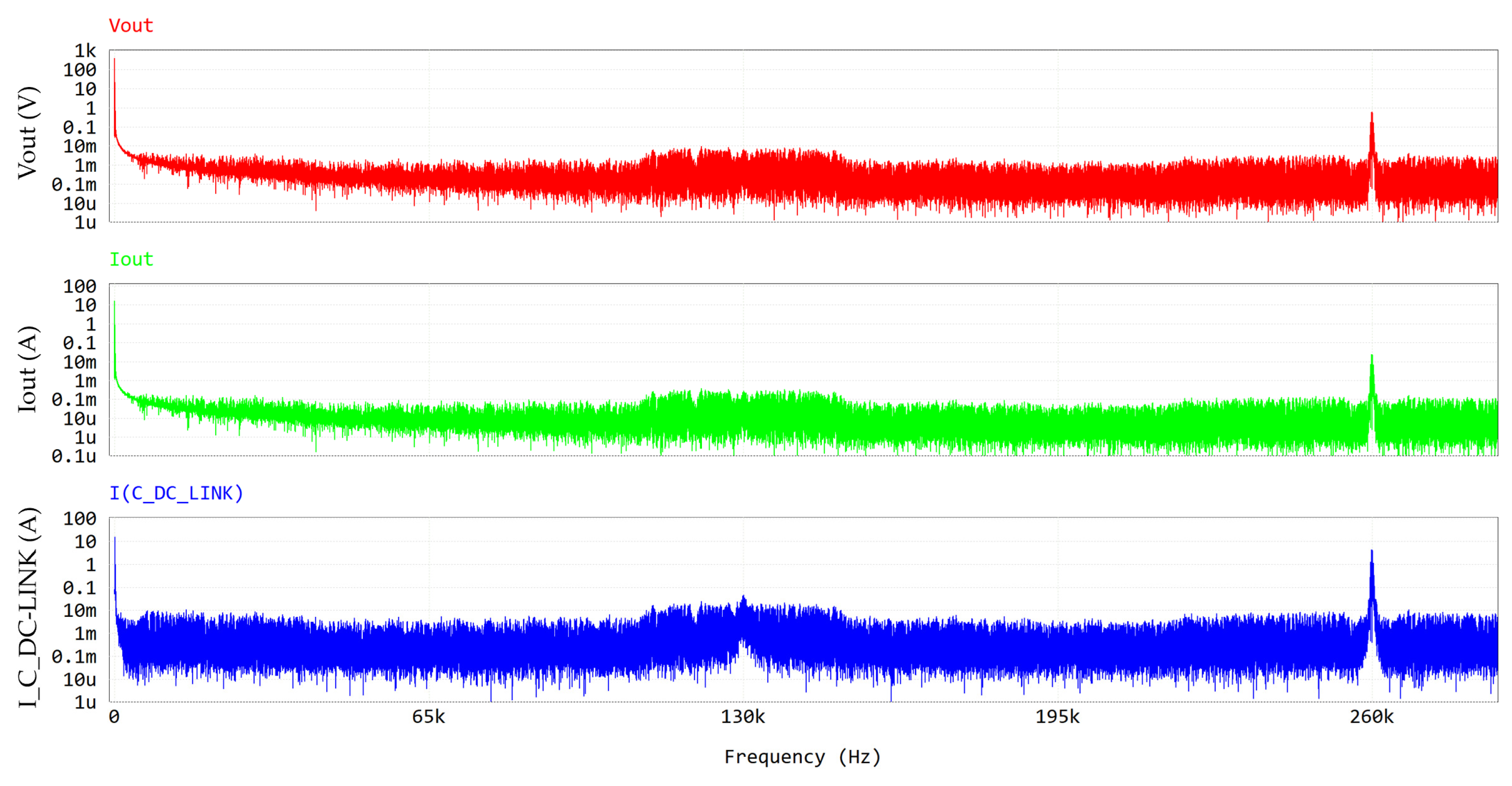
| Quantity | Amplitude (0 Hz) | Amplitude (100 Hz) | Amplitude (260 kHz) |
|---|---|---|---|
| Vout | 400 Vpk | 22.04 Vpk | 0.55 Vpk |
| Iout | 16.50 Apk | 0.91 Apk | 0.023 Apk |
| IC,DC-link | ≈0 Apk | 16 Apk | 4.41 Apk |
| Quantity | Value |
|---|---|
| Line current | 28 Arms |
| Boost inductor current | 14.27 Arms 23.17 A peak value 12.94 Apk-pk = ΔImax |
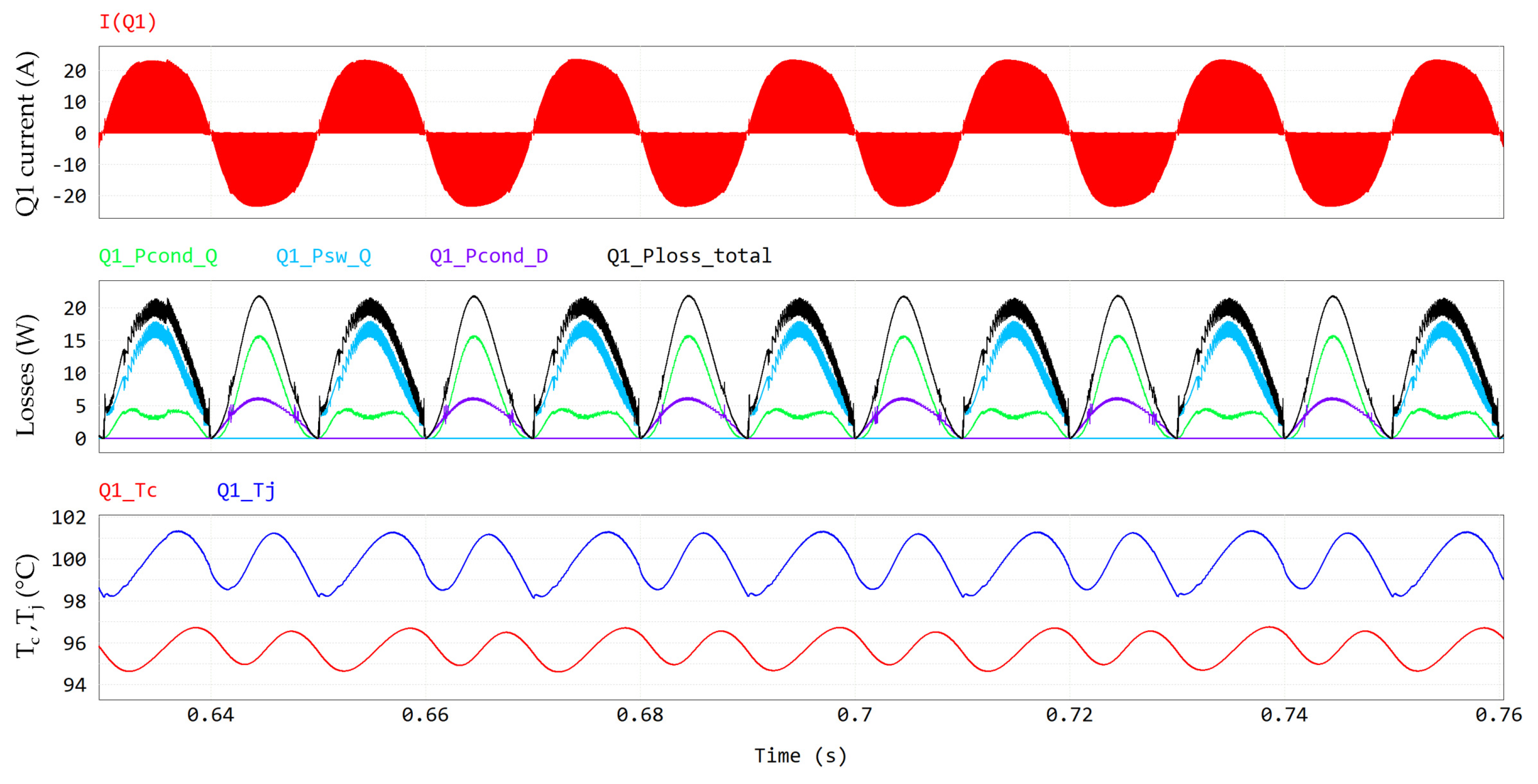
| GaN HEMT current | 10.07 Arms |
| Si mosfet current | 9.90 Arms |
| DC-link capacitor bank current | 13.32 Arms |
| GaN HEMTs temperature | Tc = 96 °C, Tj = 100 °C |
| Si mosfets temperature | Tc = 68 °C, Tj = 69 °C |
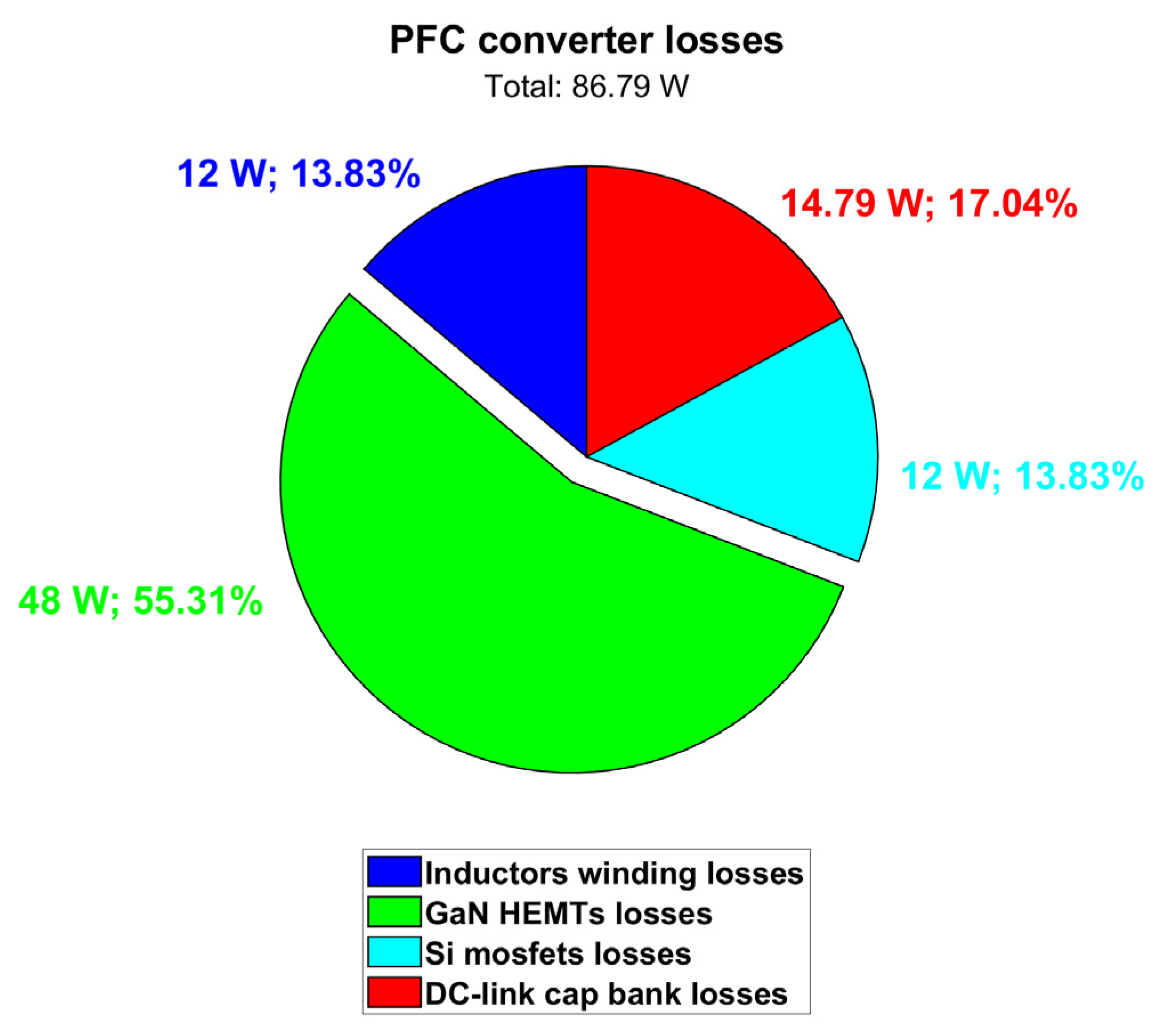
| Inductor copper losses | (2×) 6 W |
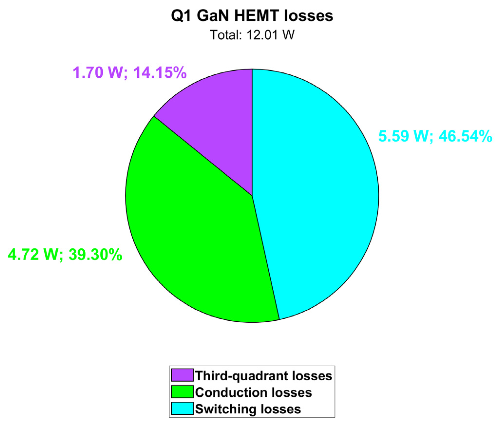
| GaN HEMTs losses | (4×) 12 W |
| Si mosfets losses | (4×) 3 W |
| DC-link capacitor bank losses | 14.79 W |
| Total losses | 86.79 W |
| Vout | 400 V |
| Vout voltage ripple | 45 Vpk-pk |
| Iout | 16.5 Arms |
| Pout | 6600 W |
| Pin | 6686.79 W |
| Efficiency | 98.70% |
| THD | 6% |
| PF | 0.996 |
| Passive Component | PN | Quantity | Parameters | |
|---|---|---|---|---|
| DAB XFMR | Bourns custom design | 1 | Cp,s = 27.2 pF Cww = 43.3 pF RDCp,s = 9.4 mΩ | Llk = 6 uH Lmag = 301.6 uH Turns ratio = 10:10 |
| 3× in the DC-link section 1× in the output section | VDC = 500 V C = 390 uF | |||
| Electrolytic capacitor | Kemet ALA7DA391CF500 | ESR = 481.2 mΩ (@ 20 °C, 10 kHz) ESL = 20 nH Icrms = 4.12 Arms (@ 85 °C, 10 kHz) | ||
| VDC = 500 V C = 1 uF | ||||
| Ceramic capacitor | TDK B58031U5105M062 | 2× for each GaN leg | ESR = 12 mΩ (@ 0 VDC, 0.5 Vrms, 25 °C, 1 MHz) ESL = 3 nH Icrms = 11 Arms (@ 85 °C, 100 kHz) | |
| Quantity | Value |
|---|---|
| XFMR current at primary | 19.21 Arms 21.21 A peak value |
| XFMR current at secondary | 19.43 Arms 21.77 A peak value |
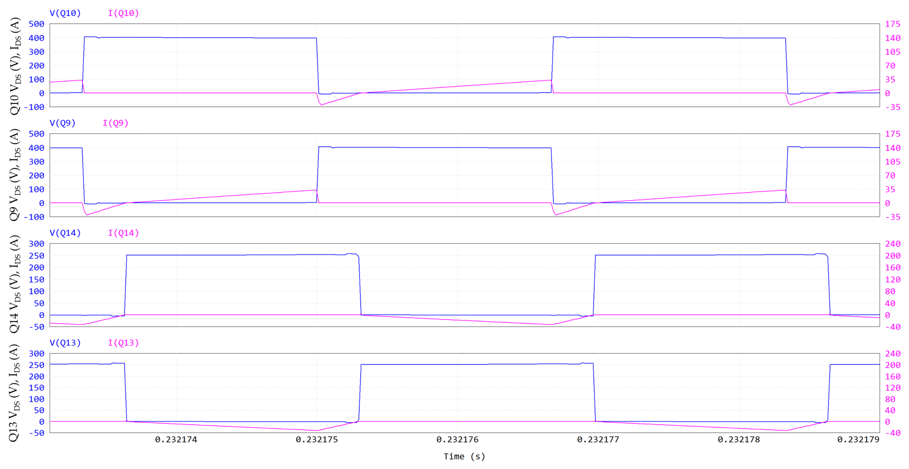
| Current of GaN HEMT at primary | 13.54 Arms 21.21 A peak value |
| Current of GaN HEMT at secondary | 13.68 Arms 21.77 A peak value |
| DC-link capacitor bank current | 3.54 Arms |
| Output capacitor current | 1.47 Arms |
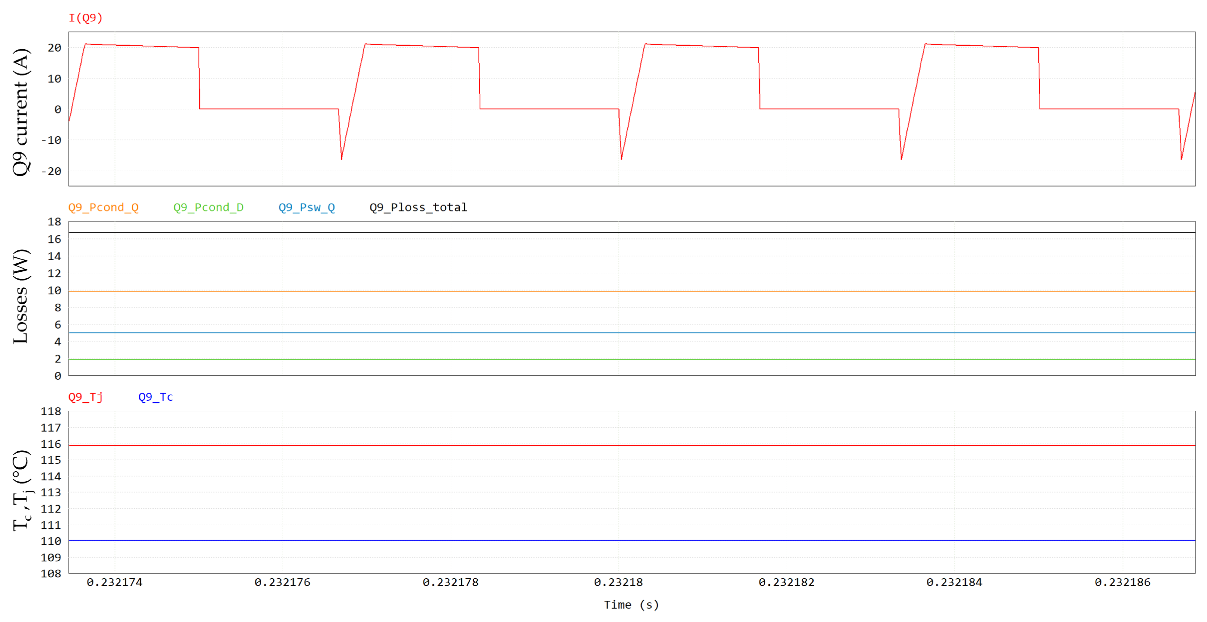
| Temperature of GaN HEMTs at primary | Tc = 110 °C, Tj = 116 °C |
| Temperature of GaN HEMTs at secondary | Tc = 117 °C, Tj = 123 °C |
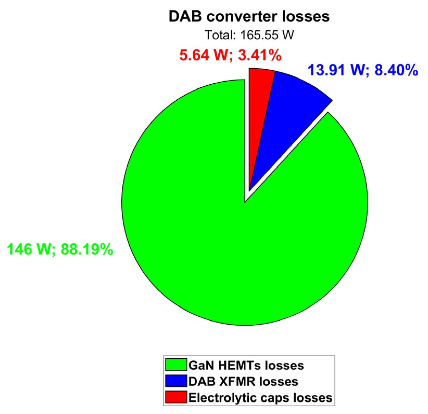
| DAB XFMR losses | 17.7 W |
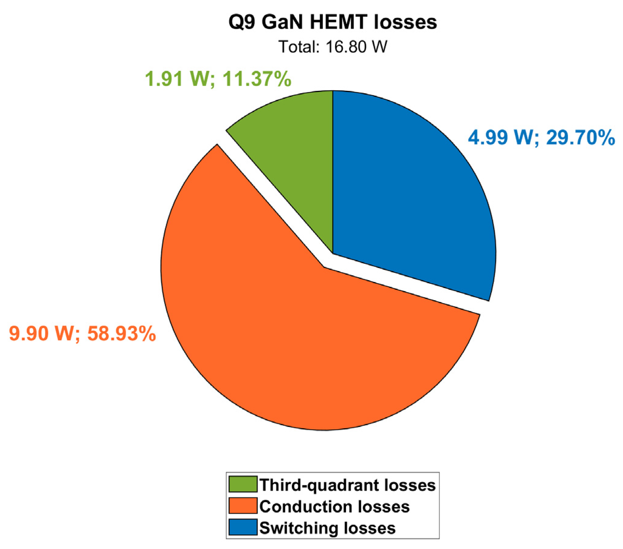
| Losses of GaN HEMTs at primary | (4×) 17 W |
| Losses of GaN HEMTs at secondary | (4×) 19 W |
| DC-link capacitor bank losses | 1.04 W |
| Output capacitor losses | 0.54 W |
| Total losses | 163.28 W |
| Vout | 400 V |
| Vout voltage ripple | 1.58 Vpk-pk |
| Iout | 16.5 Arms |
| Pout | 6600 W |
| Pin | 6763.28 W |
| Efficiency | 97.59% |
| Quantity | Value |
|---|---|
| XFMR current at primary | 19.17 Arms 33.63 A peak value |
| XFMR current at secondary | 19.06 Arms −33.44 A negative peak value |
| Current of GaN HEMT at primary | 13.45 Arms 33.63 A peak value |
| Current of GaN HEMT at secondary | 13.77 Arms −34.44 A negative peak value |
| DC-link capacitor bank current | 7.38 Arms |
| Output capacitor current | 2.10 Arms |
| Temperature of GaN HEMTs at primary | Tc = 120 °C, Tj = 127 °C |
| Temperature of GaN HEMTs at secondary | Tc = 107 °C, Tj = 113 °C |
| DAB XFMR losses | 13.91 W |
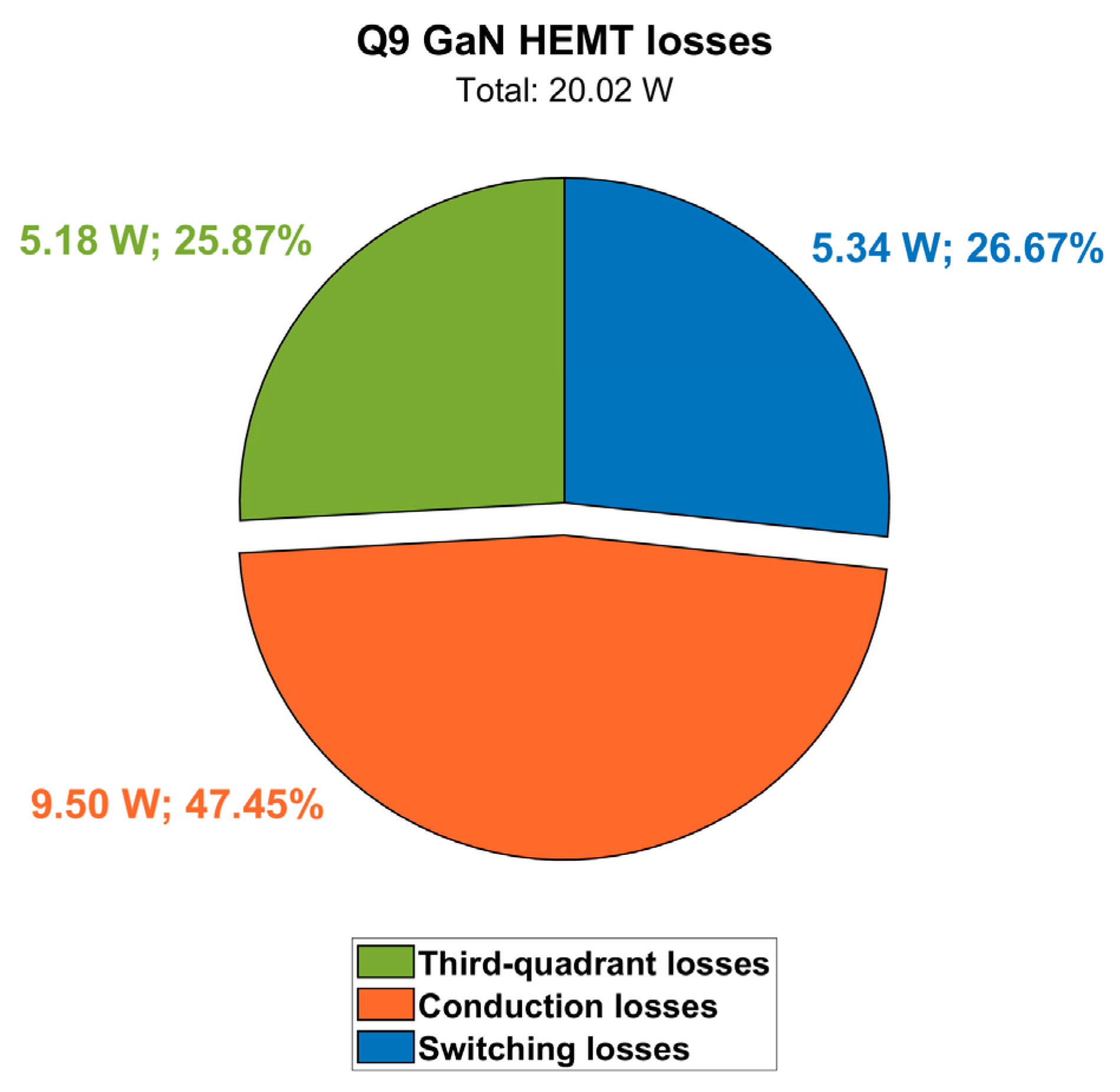
| Losses of GaN HEMTs at primary | (4×) 20 W |
| Losses of GaN HEMTs at secondary | (4×) 16.5 W |
| DC-link capacitor bank losses | 4.54 W |
| Output capacitor losses | 1.10 W |
| Total losses | 165.55 W |
| Vout | 250 V |
| Vout voltage ripple | 1.75 Vpk-pk |
| Iout | 16.5 Arms |
| Pout | 4125 W |
| Pin | 4290.55 W |
| Efficiency | 96.14% |
| DC-DC LV Stage | |||||
|---|---|---|---|---|---|
| Vin,range | Vin,nominal | Vout,range | Vout,nominal | Pout,nominal | Pout,max |
| 240–450 V | 360 V | 10–16 V | 12 V | 800 W | 1 kW |
| Passive Component | PN | Quantity | Parameters |
|---|---|---|---|
| PSFB XFMR | Bourns custom design | 1 | Lmag = 838.6 µH (@ 100 kHz) Llk = 9.3 µH (@ 100 kHz) RDC,p = 23.6 mΩ RDC,s1,s2 = 1.2 mΩ Cp,s = 14 pF Cww = 87 pF Turns ratio = 14:1:1 |
| Electrolytic input capacitor | Kemet ALA7DA391CF500 | 1 | VDC = 500 V C = 390 µF ESR = 481.2 mΩ (@ 20 °C, 10 kHz) ESL = 20 nH Icrms = 4.12 Arms (@ 85 °C, 10 kHz) |
| Ceramic capacitor | TDK B58031U5105M062 | 2× for each GaN leg at primary | VDC = 500 V C = 1 µF ESR = 12 mΩ (@ 0 VDC, 0.5 Vrms, 25 °C, 1 MHz) ESL = 3 nH Icrms = 11 Arms (@ 85 °C, 100 kHz) |
| Output inductor | Vishay IHDM1107BBEV1R1M20 | 1 | L = 1.1 µH (@ 100 kHz, 0.25 V, 0 A) DCR = 0.30 mΩ (@25 °C) Saturation current = 301 A (@ 30% of L drop) |
| Electrolytic output capacitor | Panasonic EEEFT1H331AV | 2× | VDC = 50 V C = 330 µF ESR = 120 mΩ (@ 20 °C, 100 kHz) Icrms = 0.9 Arms (@ 105 °C, 100 kHz) |
| Ceramic output capacitor | Murata GRM32ER7YA106KA12K | 5× | VDC = 35 V C = 10 µF ESR = 2 mΩ (@ 0 VDC, 25 °C, 1 MHz) |
| Quantity | Value |
|---|---|
| XFMR current at primary | 4.47 Arms 5.40 A peak value |
| XFMR current at secondary | 45.54 Arms −72.40 A negative peak value |
| Current of GaN HEMT at primary | 3.15 Arms 5.40 A peak value |
| Current of GaN switch at secondary | 45.54 Arms −72.40 A negative peak value |
| Input electrolytic capacitor current | 0.56 Arms |
| Output capacitor bank current | 2 Arms |
| Output inductor current | 66.67 Arms 71.15 A peak value 9.45 Apk-pk = ΔImax |
| Temperature of GaN HEMTs at primary | Tc = 63.1 °C, Tj = 63.6 °C |
| Temperature of eGaN FETs at secondary | Tc = 66.3 °C, Tj = 66.9 °C |
| PSFB XFMR losses | 9.75 W |
| Losses of GaN HEMTs at primary | (4×) 1.3 W |
| Losses of eGaN FETs at secondary | (4×) 2.19 W |
| Output inductor losses | 1.33 W |
| RCD snubber losses | 4.83 W |
| Total losses | 29.87 W |
| Vout | 12 V |
| Vout voltage ripple | 0.43 Vpk-pk |
| Iout | 66.67 Arms |
| Pout | 800 W |
| Pin | 829.87 W |
| Efficiency | 96.40% |
| Quantity | Measurement | Simulation | Meas. | Sim. | Meas. | Sim. | Meas. | Sim. |
|---|---|---|---|---|---|---|---|---|
| Pout | 2 kW | 2.5 kW | 3 kW | 4 kW | ||||
| Efficiency | 95.53% | 95.22% | 96.82% | 96.31% | 96% | 96.5% | 96.45% | 97% |
| THD | 4.29% | 4.35% | 2.96% | 3.11% | 2.75% | 2.84% | 2.63% | 2.77% |
| PF | 99.91% | 99.87% | 99.96% | 99.90% | 99.96% | 99.91% | 99.94% | 99.89% |
Disclaimer/Publisher’s Note: The statements, opinions and data contained in all publications are solely those of the individual author(s) and contributor(s) and not of MDPI and/or the editor(s). MDPI and/or the editor(s) disclaim responsibility for any injury to people or property resulting from any ideas, methods, instructions or products referred to in the content. |
© 2024 by the authors. Licensee MDPI, Basel, Switzerland. This article is an open access article distributed under the terms and conditions of the Creative Commons Attribution (CC BY) license (https://creativecommons.org/licenses/by/4.0/).
Share and Cite
Reali, A.; Alemanno, A.; Ronchi, F.; Rossi, C.; Florian, C. Development of GaN-Based, 6.6 kW, 450 V, Bi-Directional On-Board Charger with Integrated 1 kW, 12 V Auxiliary DC-DC Converter with High Power Density. Micromachines 2024, 15, 1470. https://doi.org/10.3390/mi15121470
Reali A, Alemanno A, Ronchi F, Rossi C, Florian C. Development of GaN-Based, 6.6 kW, 450 V, Bi-Directional On-Board Charger with Integrated 1 kW, 12 V Auxiliary DC-DC Converter with High Power Density. Micromachines. 2024; 15(12):1470. https://doi.org/10.3390/mi15121470
Chicago/Turabian StyleReali, Alessandro, Alessio Alemanno, Fabio Ronchi, Carlo Rossi, and Corrado Florian. 2024. "Development of GaN-Based, 6.6 kW, 450 V, Bi-Directional On-Board Charger with Integrated 1 kW, 12 V Auxiliary DC-DC Converter with High Power Density" Micromachines 15, no. 12: 1470. https://doi.org/10.3390/mi15121470
APA StyleReali, A., Alemanno, A., Ronchi, F., Rossi, C., & Florian, C. (2024). Development of GaN-Based, 6.6 kW, 450 V, Bi-Directional On-Board Charger with Integrated 1 kW, 12 V Auxiliary DC-DC Converter with High Power Density. Micromachines, 15(12), 1470. https://doi.org/10.3390/mi15121470