
Design of Inner Matching Three-Stage High-Power Doherty Power Amplifier Based on GaN HEMT Model
Abstract
1. Introduction
2. Materials and Methods
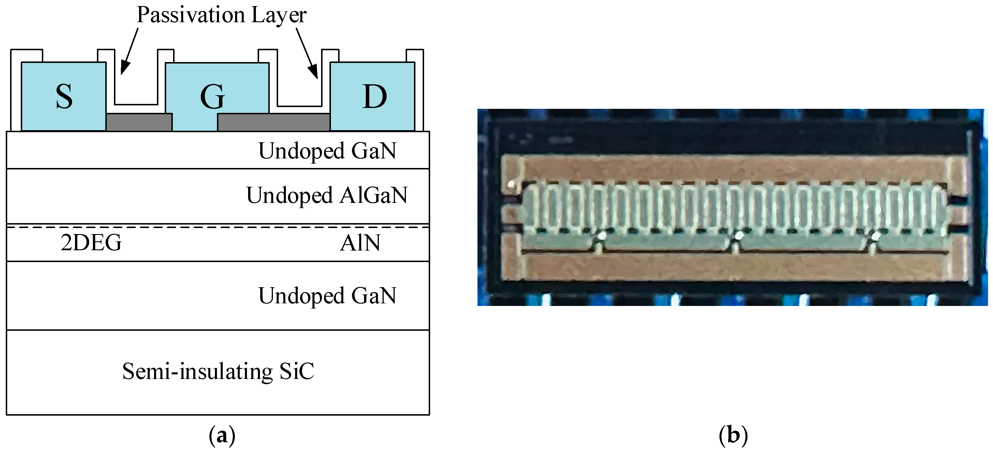
2.1. Introduction of GaN HEMT Devices
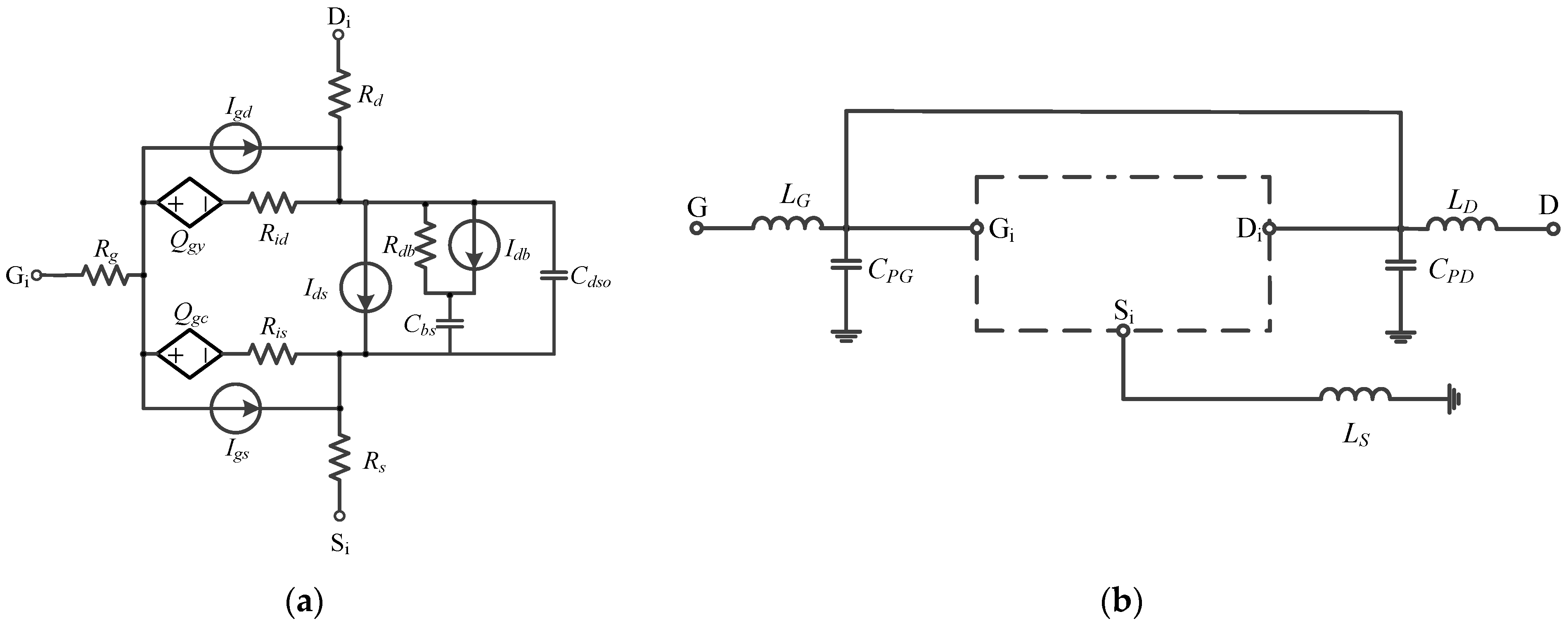
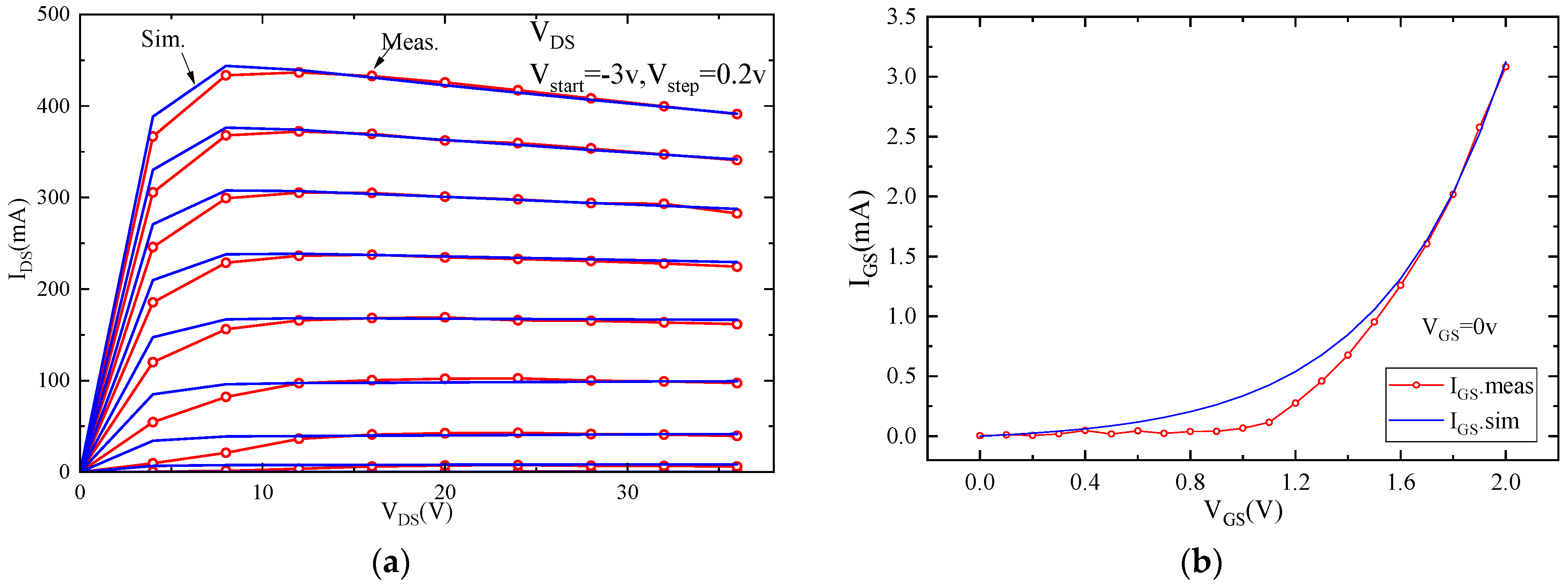
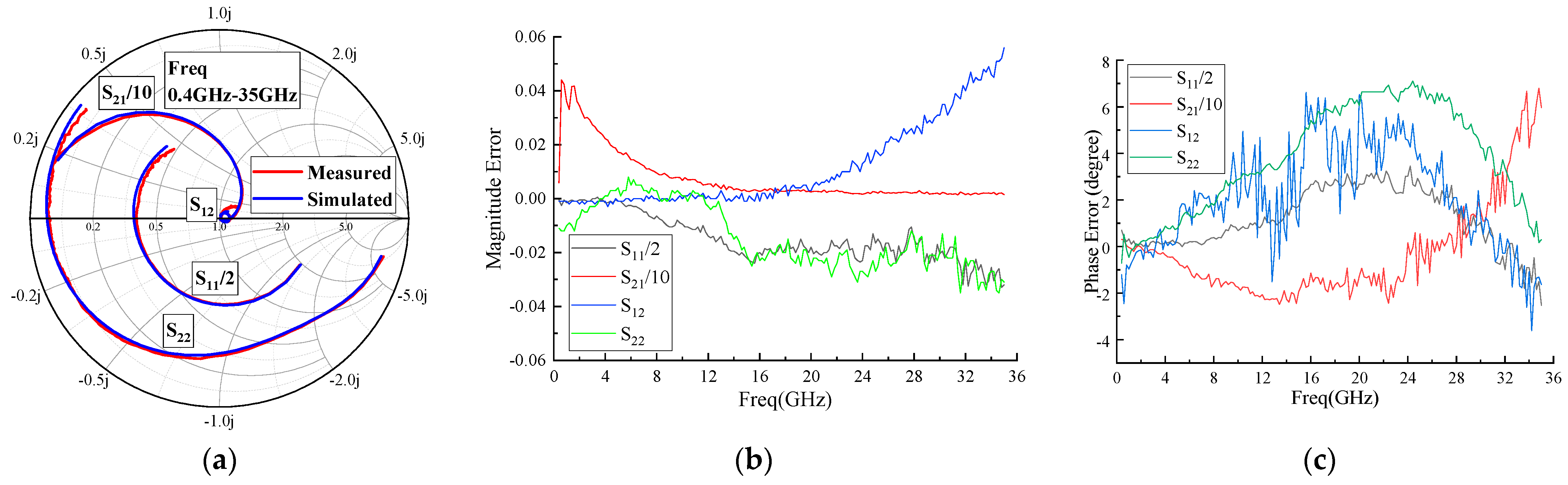
2.2. Parameter Extraction and Model Establishment
2.3. Theory and Circuit
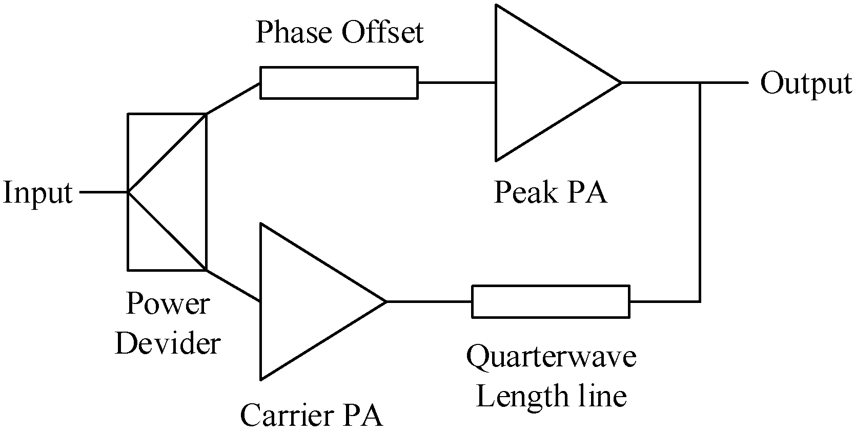
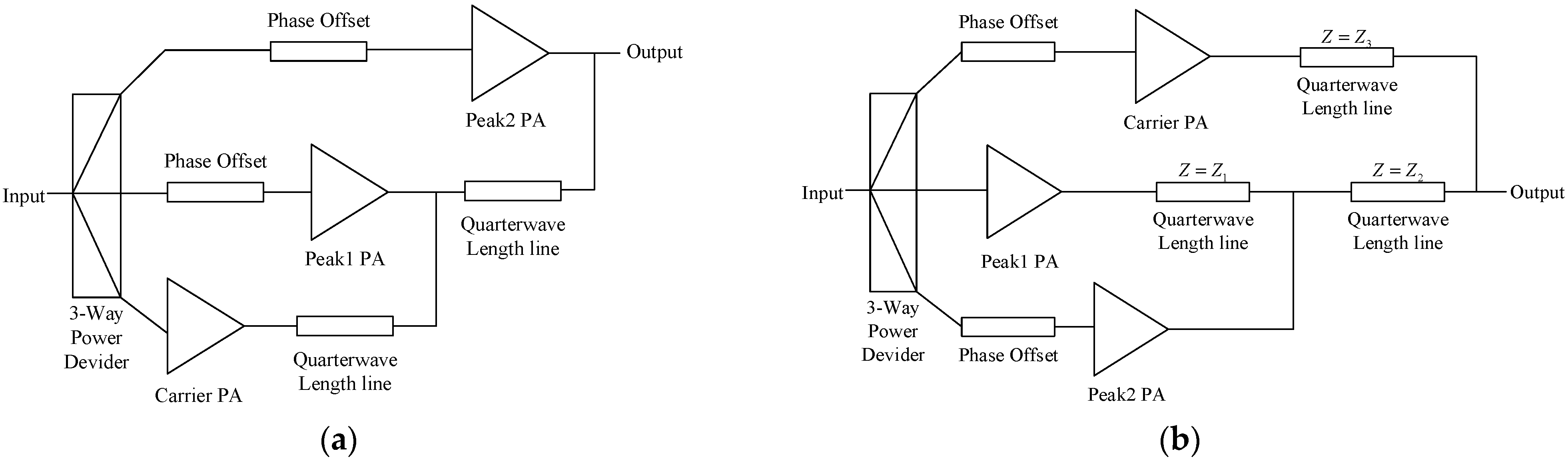
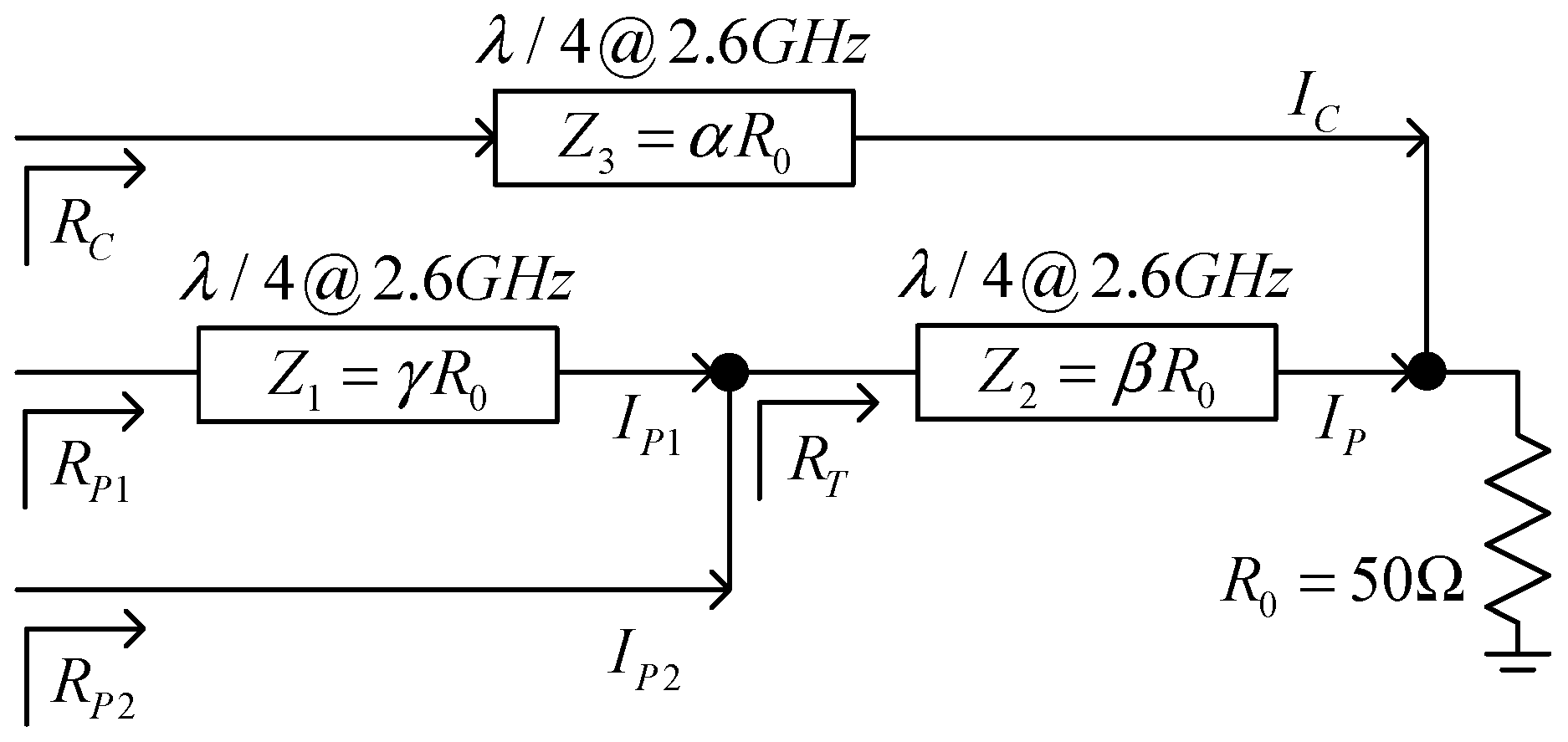
2.3.1. Load Modulation Behavior Analysis of Three-Stage Doherty PA
= 1/2·α2·R0 vin/vmax = 2/3
= 1/3·α2·R0 vin/vmax = 1
= 3·γ2·R0/β2 vin/vmax = 2/3
= 3/4·γ2·R0/β2 vin/vmax = 1
= ∞ vin/vmax = 2/3
= 4/3·β2·R0 vin/vmax = 1
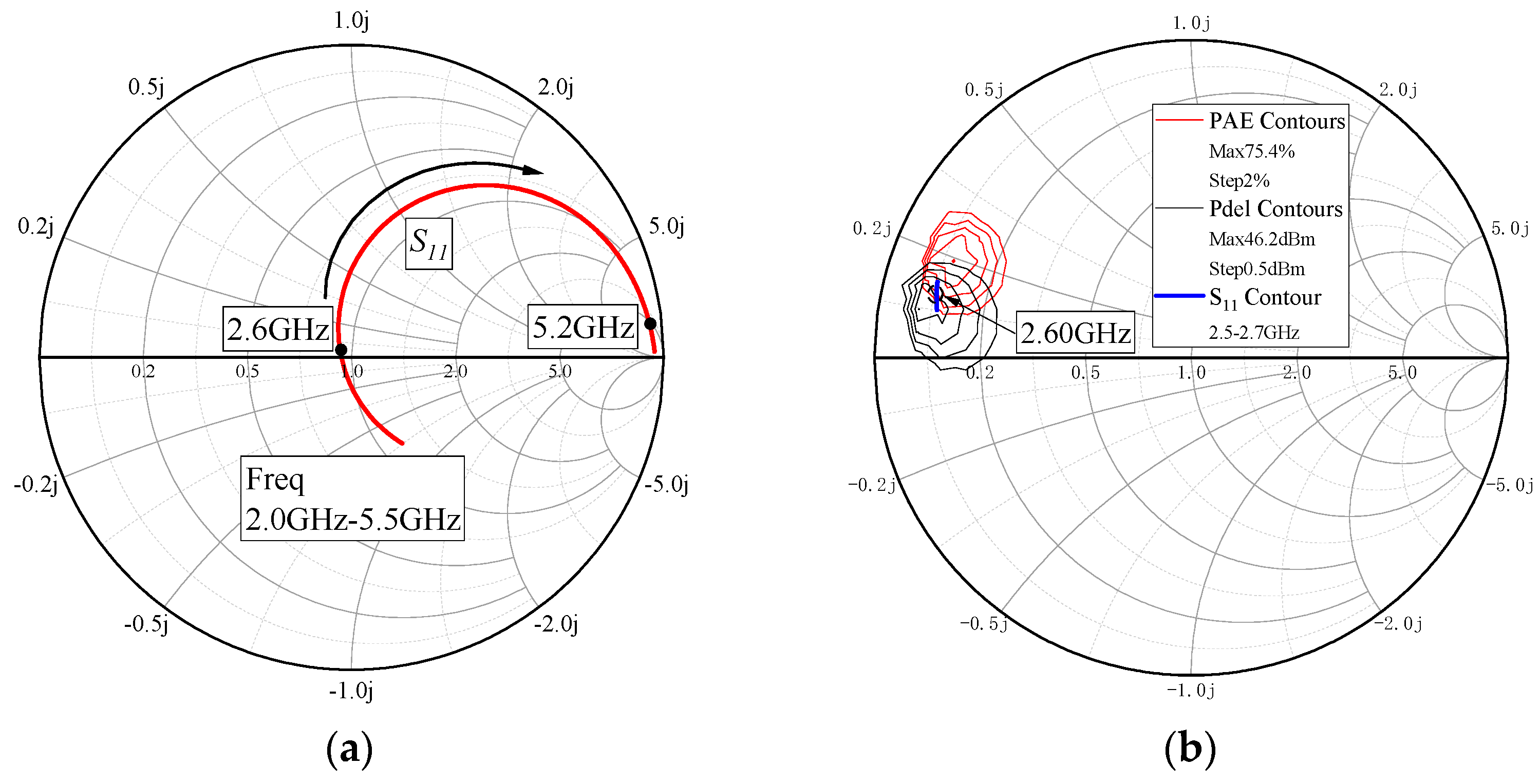
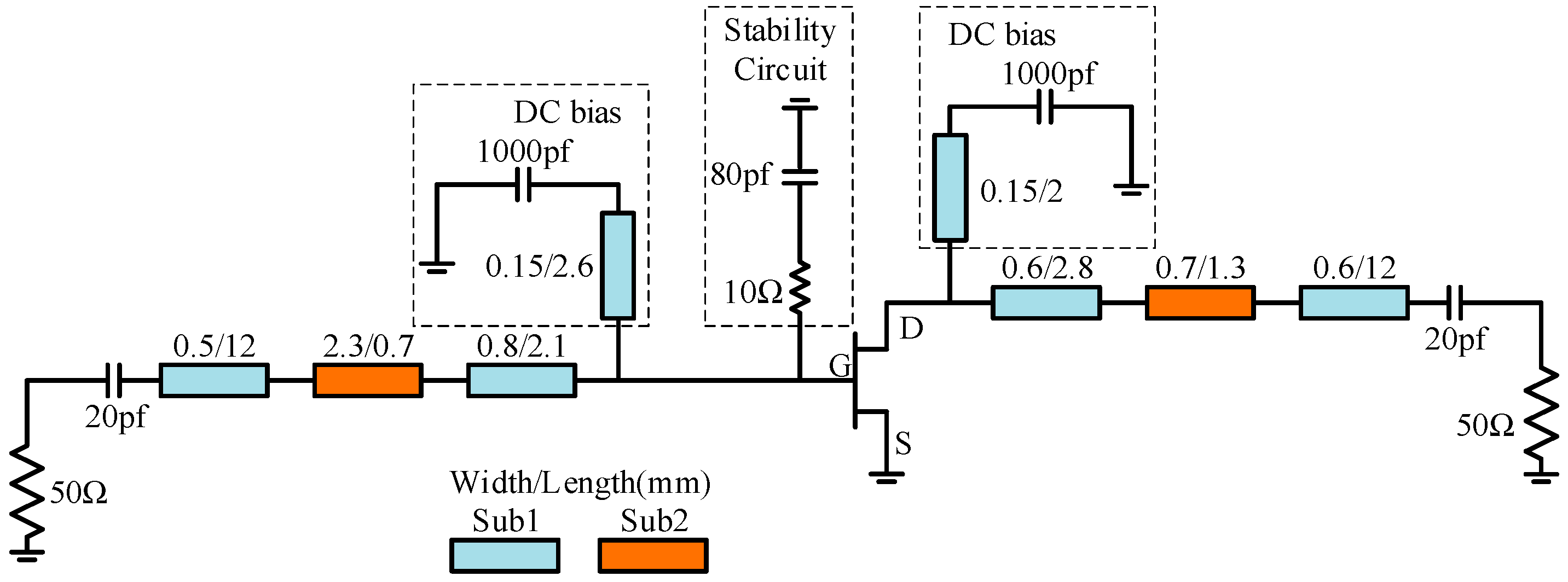
2.3.2. Circuit Design
3. Results
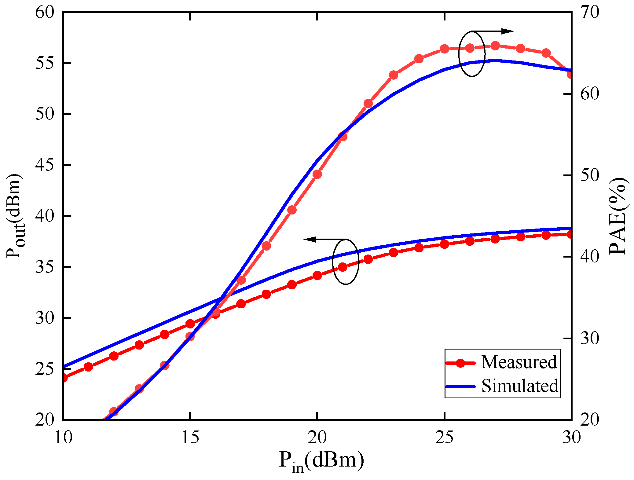
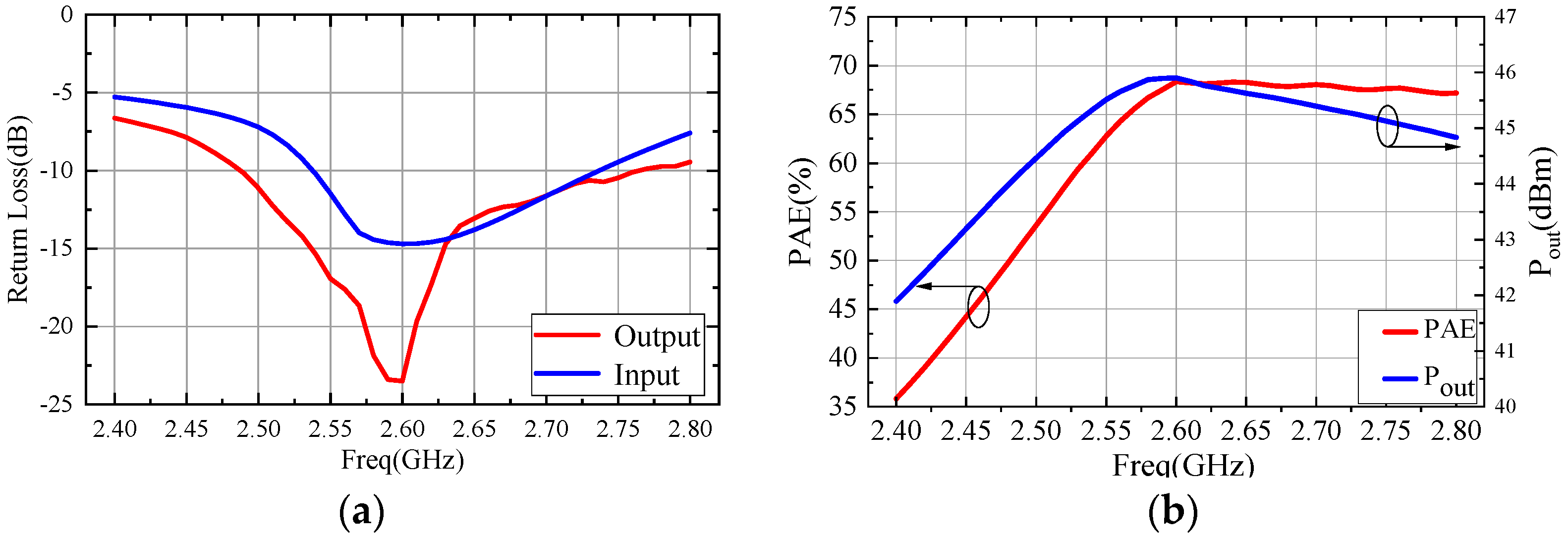
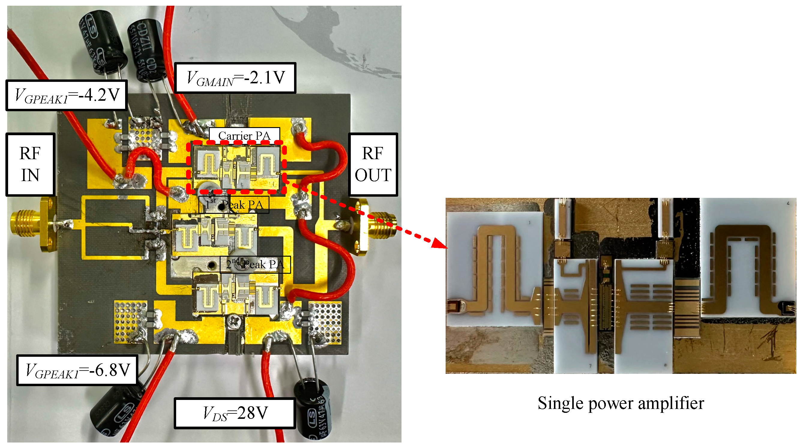
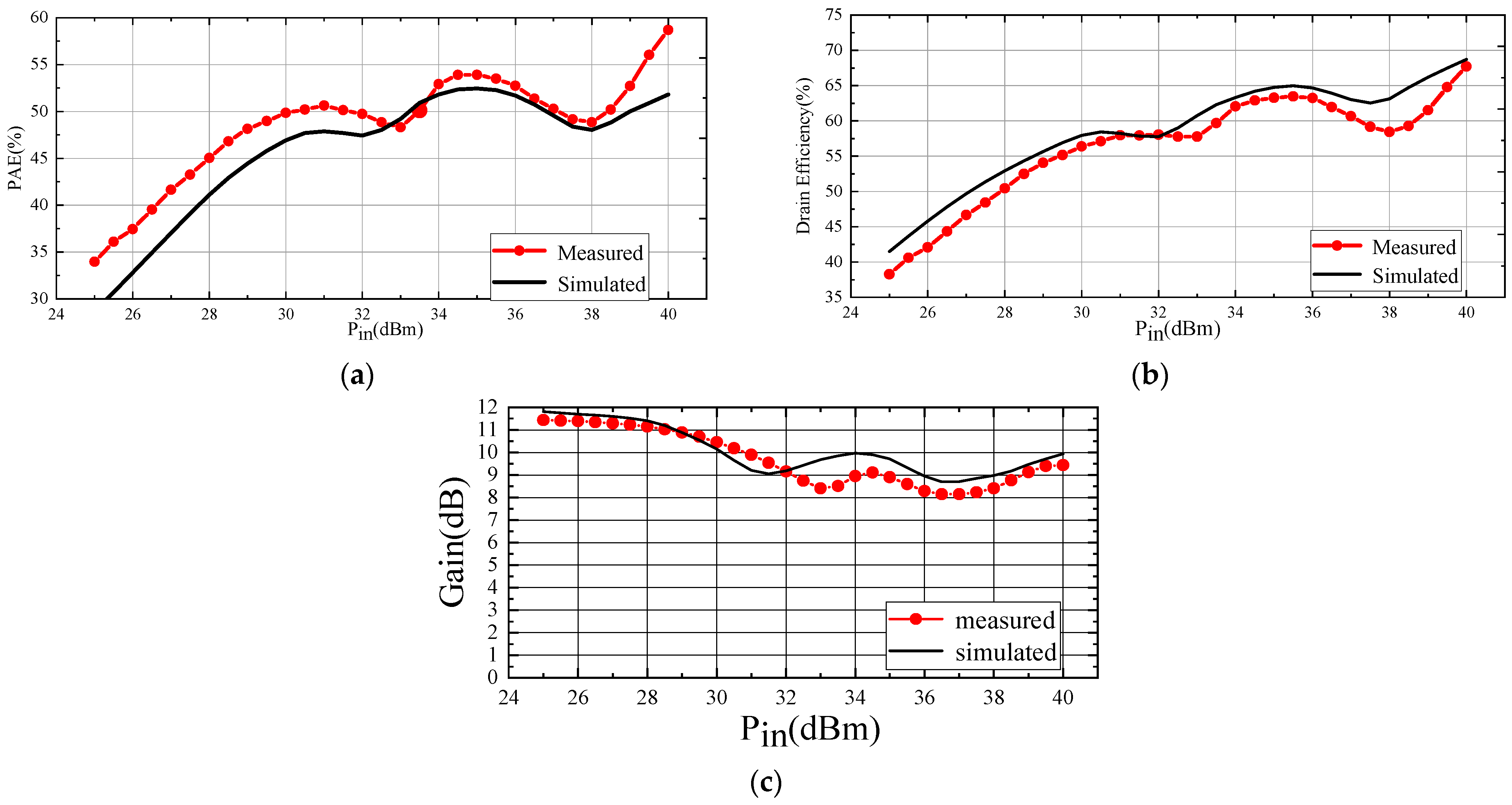
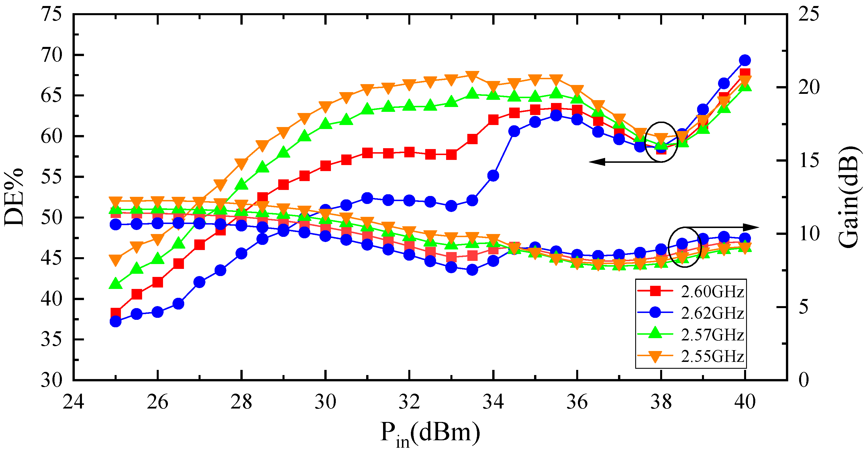
3.1. CW Test
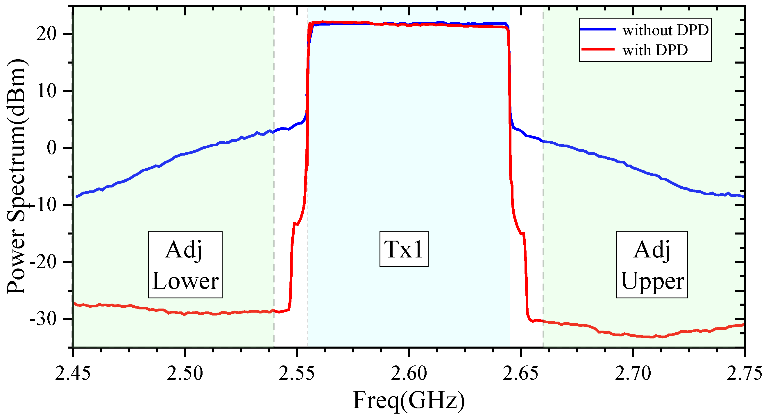
3.2. Modulated Signal Test
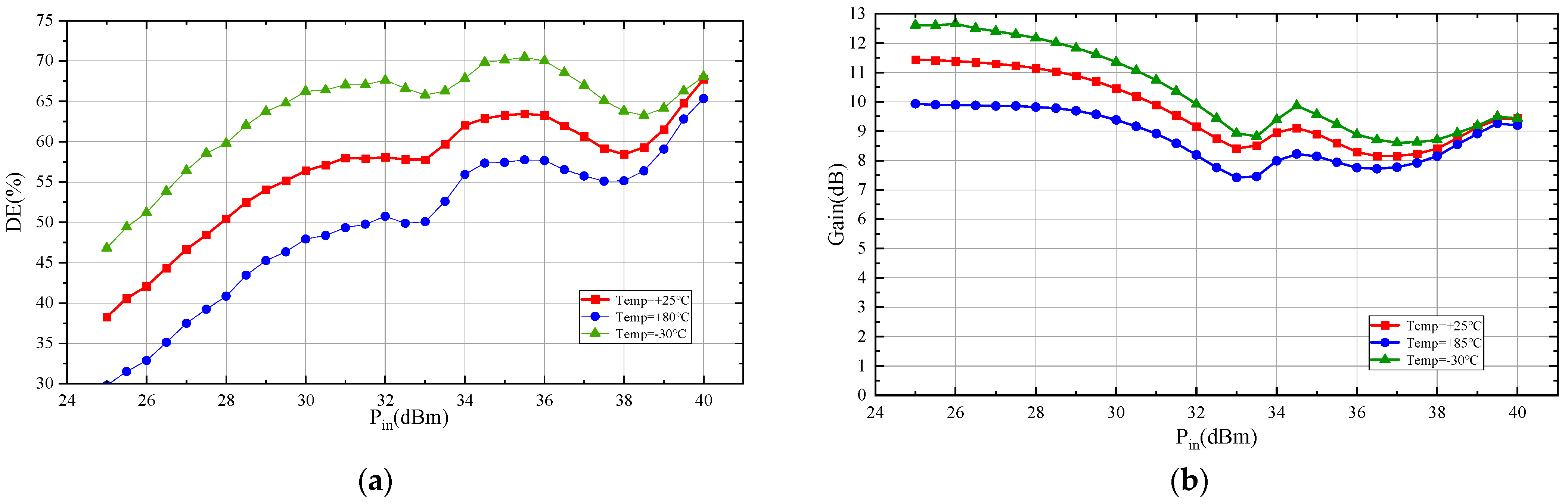
3.3. Temperature Test and Aging Test
4. Discussion
5. Conclusions
Author Contributions
Funding
Data Availability Statement
Conflicts of Interest
References
- Mohammady, S.; Farrell, R.; Malone, D.; Dooley, J. Performance Investigation of Peak Shrinking and Interpolating the PAPR Reduction Technique for LTE-Advance and 5G Signals. Information 2020, 11, 20. [Google Scholar] [CrossRef]
- Bangerter, B.; Talwar, S.; Arefi, R.; Stewart, K. Networks and devices for the 5G era(Article). IEEE Commun. Mag. 2014, 52, 90–96. [Google Scholar] [CrossRef]
- Doherty, W.H. A New High Efficiency Power Amplifier for Modulated Waves. Proc. IRE 1936, 24, 1163–1182. [Google Scholar] [CrossRef]
- Giofrè, R.; Piazzon, L.; Colantonio, P.; Giannini, F. An ultra-broadband GaN Doherty amplifier with 83% of fractional bandwidth. IEEE Microw. Wirel. Compon. Lett. 2014, 24, 775–777. [Google Scholar] [CrossRef]
- Giofrè, R.; Piazzon, L.; Colantonio, P.; Giannini, F. A closed-form design technique for ultra-wideband Doherty power amplifiers. IEEE Trans. Microw. Theory Tech. 2014, 62, 3414–3424. [Google Scholar] [CrossRef]
- Zhang, J.R.; Zheng, S.Y.; Yang, N. An Efficient Broadband Symmetrical Doherty Power Amplifier With Extended Back-Off Range. IEEE Trans. Circuits Syst. II Express Briefs 2023, 70, 1316–1320. [Google Scholar] [CrossRef]
- Oh, H.; Kang, H.; Lee, H.; Koo, H.; Kim, M.; Lee, W.; Lim, W.; Park, C.-S.; Hwang, K.C.; Lee, K.-Y.; et al. Doherty Power Amplifier Based on the Fundamental Current Ratio for Asymmetric cells. IEEE Trans. Microw. Theory Tech. 2017, 65, 4190–4197. [Google Scholar] [CrossRef]
- Pitt, A.; Jindal, G.; Morris, K.; Cappello, T. A Broadband Asymmetrical Doherty Power Amplifier With Optimized Continuous Mode Harmonic Impedances. IEEE J. Microw. 2023, 3, 1120–1133. [Google Scholar] [CrossRef]
- Zhang, Z.; Fusco, V.; Cheng, Z.; Gu, C.; Buchanan, N.; Ying, J. A Broadband Doherty-like Power Amplifier With Large Power Back-Off Range. IEEE Trans. Circuits Syst. II Express Briefs 2022, 69, 2722–2726. [Google Scholar] [CrossRef]
- Zhou, L.H.; Zhou, X.Y.; Chan, W.S. A Compact and Broadband Doherty Power Amplifier Without Post-Matching Network. IEEE Trans. Circuits Syst. II Express Briefs 2023, 70, 919–923. [Google Scholar] [CrossRef]
- Bai, G.; Dai, Z.; Wang, J.; Bi, C.; Shi, W.; Pang, J.; Li, M. Design of Broadband Doherty Power Amplifier Based on Single Loop Load Modulation Network. IEEE J. Emerg. Sel. Top. Circuits Syst. 2024. [Google Scholar] [CrossRef]
- Moreno Rubio, J.J.; Angarita Malaver, E.F.; Lara González, L.Á. Wideband Doherty Power Amplifier: A Design Approach. Micromachines 2022, 13, 497. [Google Scholar] [CrossRef]
- Xie, L.; Zhong, S.; Liang, C. High-efficiency broadband Doherty amplifier based on internal matching. Microw. Opt. Technol. Lett. 2023, 66, e33877. [Google Scholar] [CrossRef]
- Liang, C.; Roblin, P.; Hahn, Y. Accelerated Design Methodology for Dual-Input Doherty Power Amplifiers. IEEE Trans. Microw. Theory Tech. 2019, 67, 3983–3995. [Google Scholar] [CrossRef]
- Wu, D.Y.-T.; Boumaiza, S. A Modified Doherty Configuration for Broadband Amplification Using Symmetrical Devices. IEEE Trans. Microw. Theory Tech. 2012, 60, 3201–3213. [Google Scholar] [CrossRef]
- Kim, I.; Moon, J.; Jee, S.; Kim, B. Optimized Design of a Highly Efficient Three-Stage Doherty PA Using Gate Adaptation. IEEE Trans. Microw. Theory Tech. 2010, 58, 2562–2574. [Google Scholar] [CrossRef]
- Barthwal, A.; Rawat, K.; Koul, S. Bandwidth Enhancement of Three-Stage Doherty Power Amplifier Using Symmetric Devices. IEEE Trans. Microw. Theory Tech. 2015, 63, 2399–2410. [Google Scholar] [CrossRef]
- Naderi, P.; Fallahi, F. A Design Strategy for Bandwidth Enhancement in Three-Stage Doherty Power Amplifier with Extended Dynamic Range. IEEE Trans. Microw. Theory Tech. 2018, 66, 1024–1033. [Google Scholar]
- Zhou, H.; Perez-Cisneros, J.R.; Hesami, S.; Buisman, K.; Fager, C. A Generic Theory for Design of Efficient Three-Stage Doherty Power Amplifiers. IEEE Trans. Microw. Theory Tech. 2022, 70, 1242–1253. [Google Scholar] [CrossRef]
- Xia, J.; Chen, W.; Meng, F.; Yu, C.; Zhu, X. Improved Three-Stage Doherty Amplifier Design With Impedance Compensation in Load Combiner for Broadband Applications. IEEE Trans. Microw. Theory Tech. 2019, 67, 778–786. [Google Scholar] [CrossRef]
- Meghdadi, M.; Medi, A. Design of 6–18-GHz High-Power Amplifier in GaAs pHEMT Technology. IEEE Trans. Microw. Theory Tech. 2017, 65, 2353–2360. [Google Scholar] [CrossRef]
- Chen, Y.; Liu, W.; Wang, C.; Kong, X.; Zhao, Z. A scalable non-linear compact model applied to HEMT devices. J. Terahertz Sci. Electron. Inf. Technol. 2019, 17, 162–168. [Google Scholar]
- Huang, D.; Zhong, S.C.; Xu, Z.Y.; Cheng, A.Q.; Wang, S. Research on Nonlinear Behavior Model of GaN HEMT Based on EPHD. Radio Eng. 2022, 52, 1490–1495. [Google Scholar]
- Kharabi, F.; Poulton, M.J.; Halchin, D.; Green, D. A Classic Nonlinear FET model for GaN HEMT Devices. In Proceedings of the 2007 IEEE Compound Semiconductor Integrated Circuits Symposium, Portland, OR, USA, 14–17 October 2007. [Google Scholar]
- Zomorrodian, V.; Pei, Y.; Mishra, U.K.; York, R.A. A scalable EE_HEMT based large signal model for multi-finger AlGaN/GaN HEMTs for linear and non-linear circuit design. Phys. Status Solidi C 2010, 7, 2450–2454. [Google Scholar] [CrossRef]
- He, J.; Zhong, S.C.; Zhu, J.; Zhang, H.C. Design of an L-band high-elicieney small-size power amplifier carrier. Space Electron. Technol. 2023, 20, 24–28. [Google Scholar]
- Shao, G.; Zhao, Y.; Wang, J.; Zhou, S.; Chen, T.; Jing, S.; Zhong, S. Study on 60Co-γ Irradiation Effect of GaN HEMT Devices. Res. Prog. SSE 2023, 43, 277–280, 286. [Google Scholar]


| vin/vmax | 1/3 | 2/3 | 1 |
|---|---|---|---|
| δ1 | 0 | 1 | 2 |
| δ2 | 0 | 0 | 1 |
| Units | Architecture | f0 (GHz) | BW (MHz) | PMAX (dBm) | DE (%) @PBO | Back-Off Range | ACLR |
|---|---|---|---|---|---|---|---|
| [6] | 2-way | 2.43 | 750 | 44.6 | 49 | 9 | −46.2 dBc |
| [7] | 2-way | 2.14 | 10 | 36.9 | 55.7 | 6.5 | −25.0 dBc |
| [16] | 3-stage | 2.655 | 15 | 50.5 | 55.4 | 8.5 | −40 dBc |
| [18] | 3-stage | 0.75 | 300 | 46.1 | 50 | 12 | −50.2 dBc |
| [19] | 3-stage | 2.14 | 100 | 45.3 | 55 | 10 | −49.8 dBc |
| [20] | 3-way | 2.1 | 600 | 46 | 53 | 9.5 | −30 dBc |
| This work | 3-stage | 2.6 | 70 | 49.7 | 57.9 | 9 | −50.93 dBc |
Disclaimer/Publisher’s Note: The statements, opinions and data contained in all publications are solely those of the individual author(s) and contributor(s) and not of MDPI and/or the editor(s). MDPI and/or the editor(s) disclaim responsibility for any injury to people or property resulting from any ideas, methods, instructions or products referred to in the content. |
© 2024 by the authors. Licensee MDPI, Basel, Switzerland. This article is an open access article distributed under the terms and conditions of the Creative Commons Attribution (CC BY) license (https://creativecommons.org/licenses/by/4.0/).
Share and Cite
Li, R.; Ge, C.; Liang, C.; Zhong, S. Design of Inner Matching Three-Stage High-Power Doherty Power Amplifier Based on GaN HEMT Model. Micromachines 2024, 15, 388. https://doi.org/10.3390/mi15030388
Li R, Ge C, Liang C, Zhong S. Design of Inner Matching Three-Stage High-Power Doherty Power Amplifier Based on GaN HEMT Model. Micromachines. 2024; 15(3):388. https://doi.org/10.3390/mi15030388
Chicago/Turabian StyleLi, Renyi, Chen Ge, Chenwei Liang, and Shichang Zhong. 2024. "Design of Inner Matching Three-Stage High-Power Doherty Power Amplifier Based on GaN HEMT Model" Micromachines 15, no. 3: 388. https://doi.org/10.3390/mi15030388
APA StyleLi, R., Ge, C., Liang, C., & Zhong, S. (2024). Design of Inner Matching Three-Stage High-Power Doherty Power Amplifier Based on GaN HEMT Model. Micromachines, 15(3), 388. https://doi.org/10.3390/mi15030388