
Effect of Grain Size on Nanometric Cutting of Polycrystalline Silicon via Molecular Dynamics Simulation


Abstract
:1. Introduction
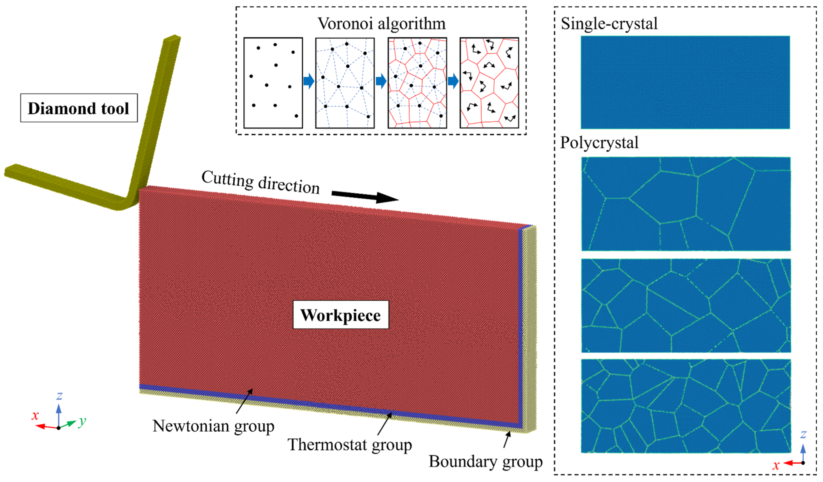
2. Methodology
3. Results and Discussion
3.1. Material Removal Behavior
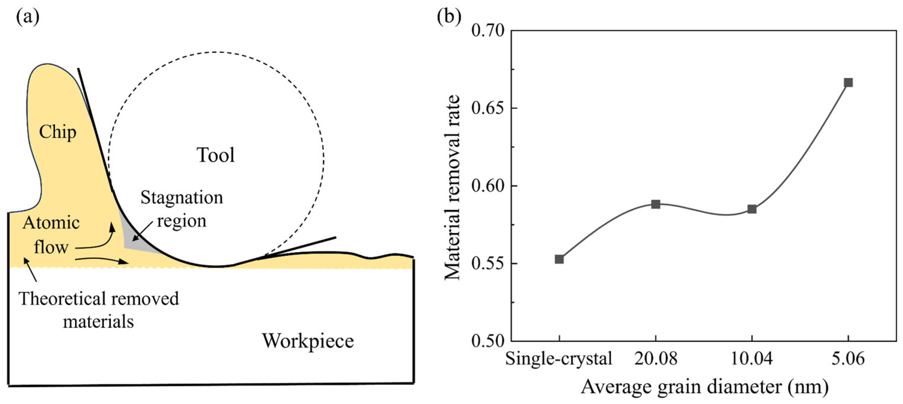
3.1.1. Atomic Flow
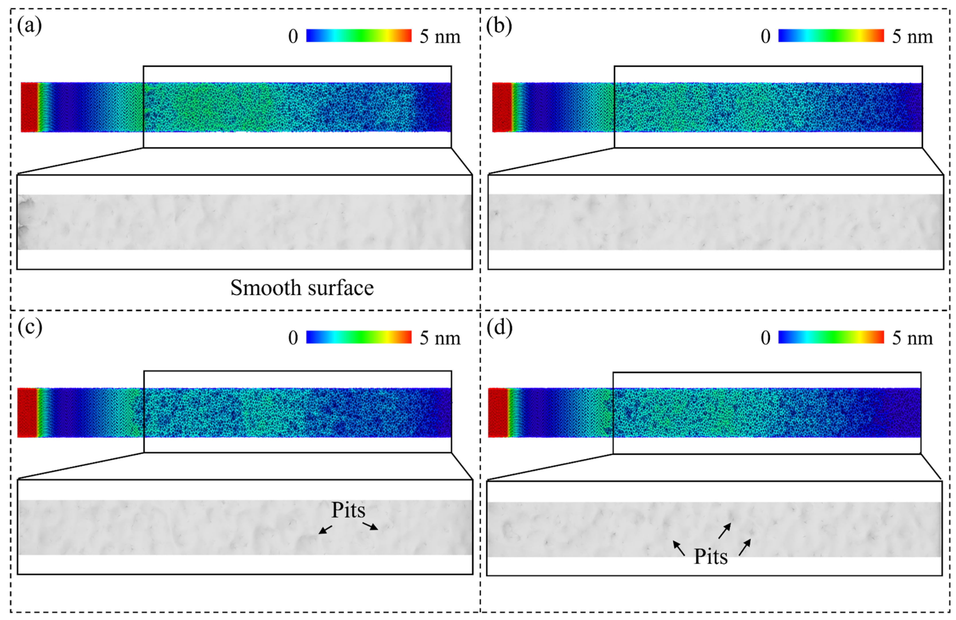
3.1.2. Surface Morphology
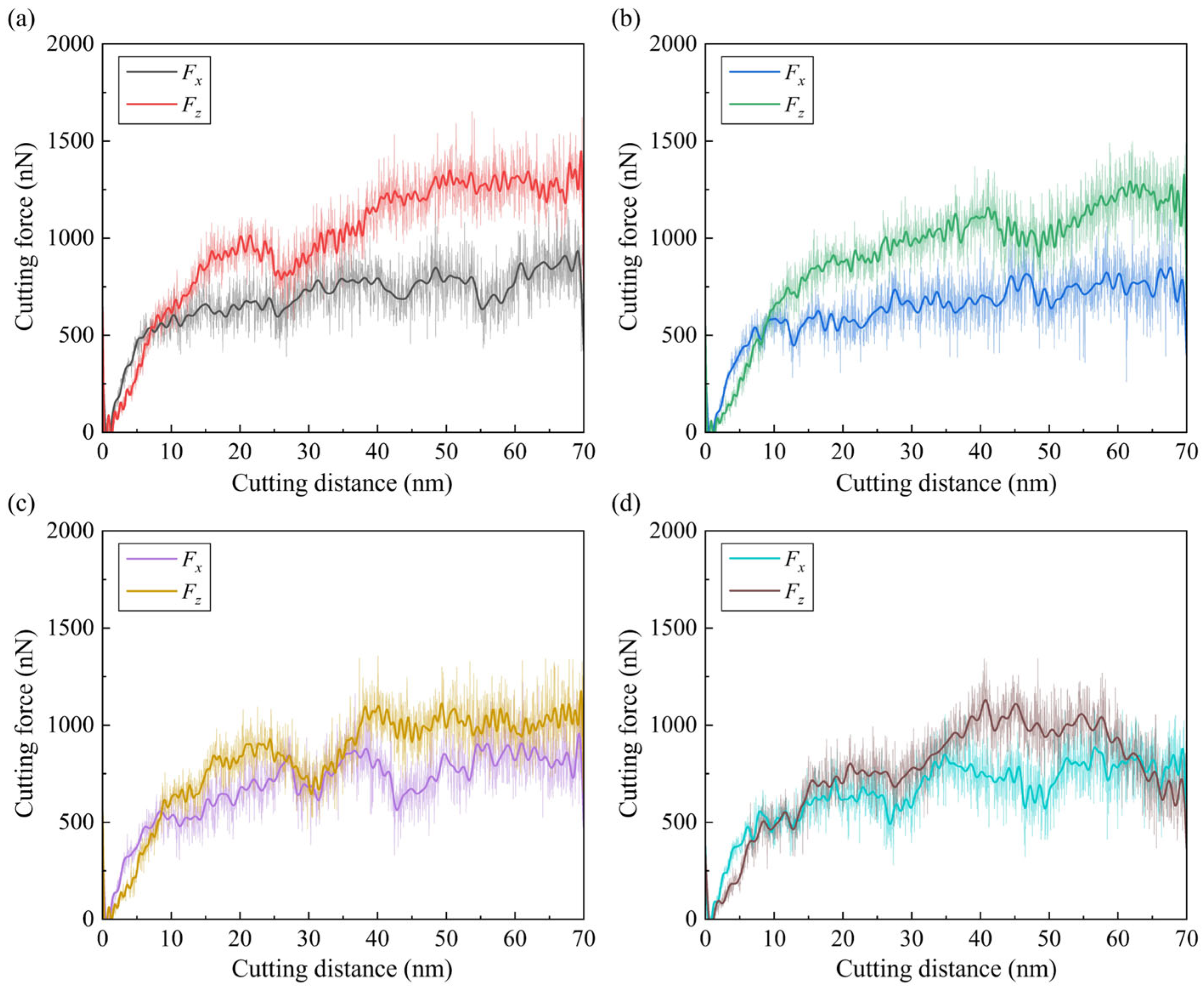
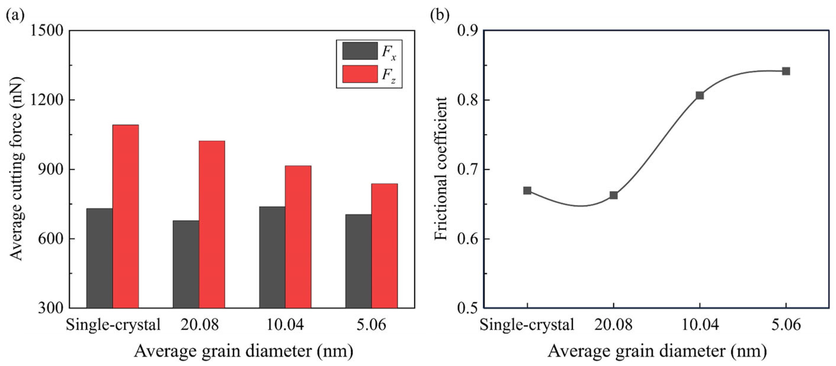
3.1.3. Cutting Force
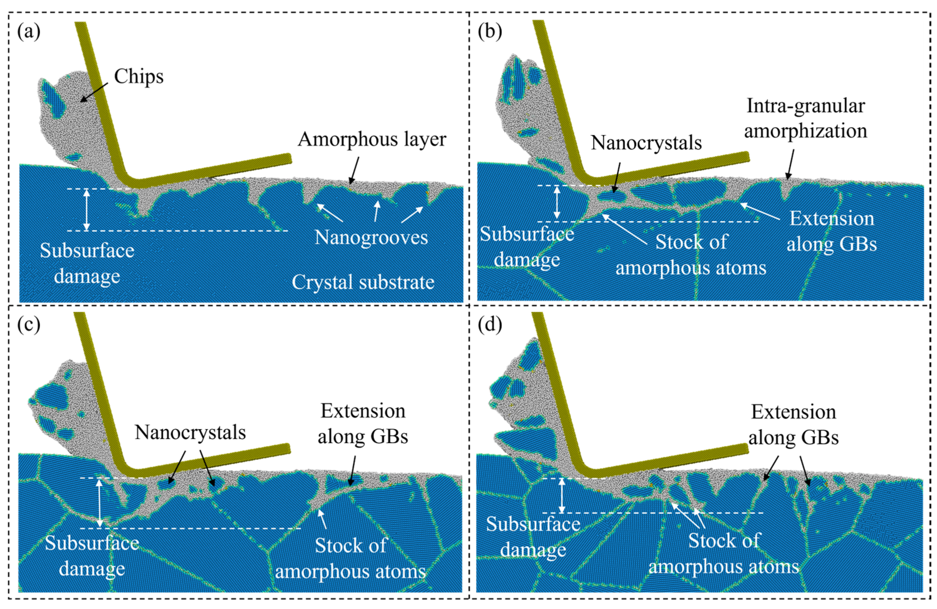
3.2. Subsurface Damage Formation
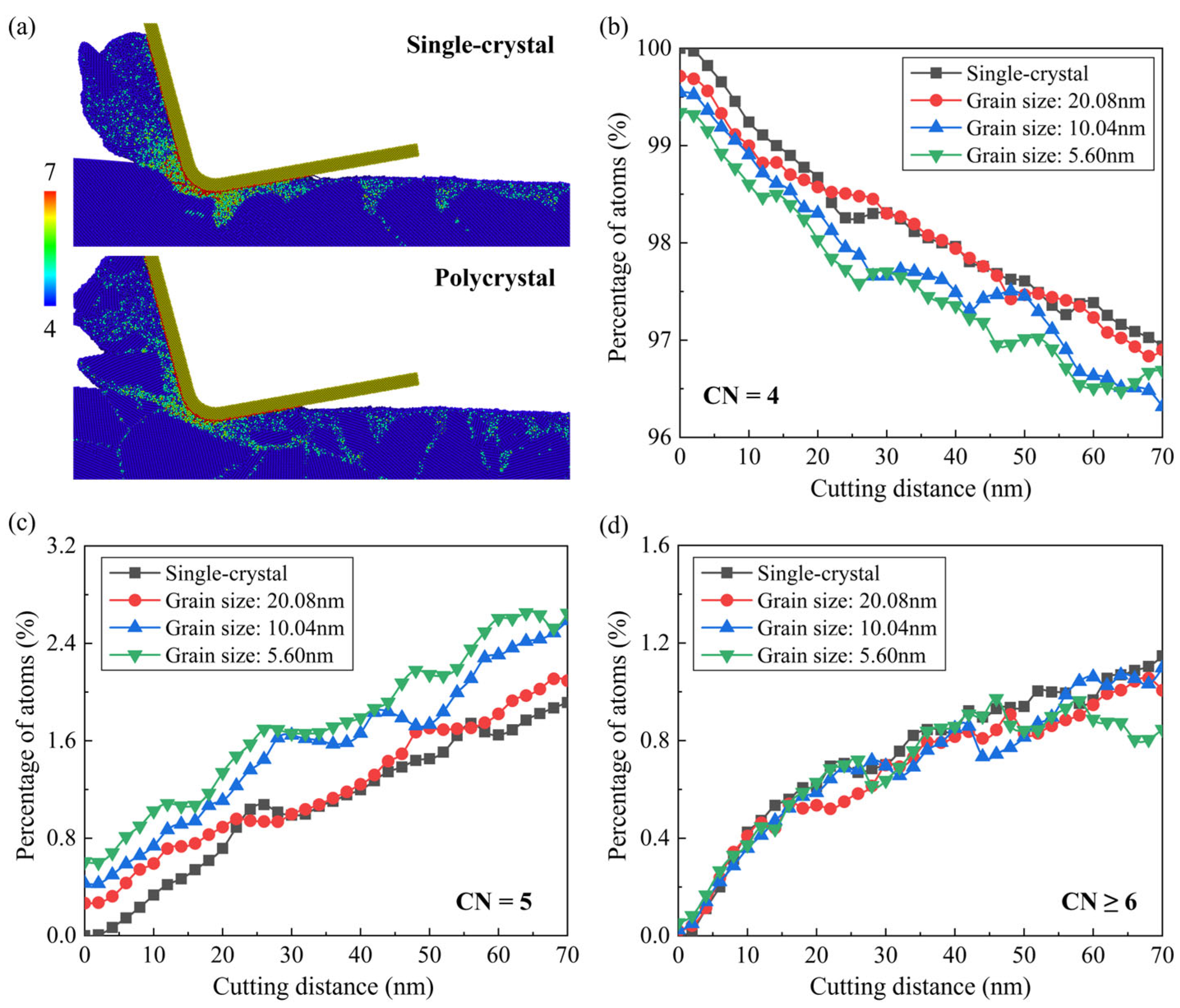
3.2.1. Plastic Deformation
3.2.2. Phase Transition
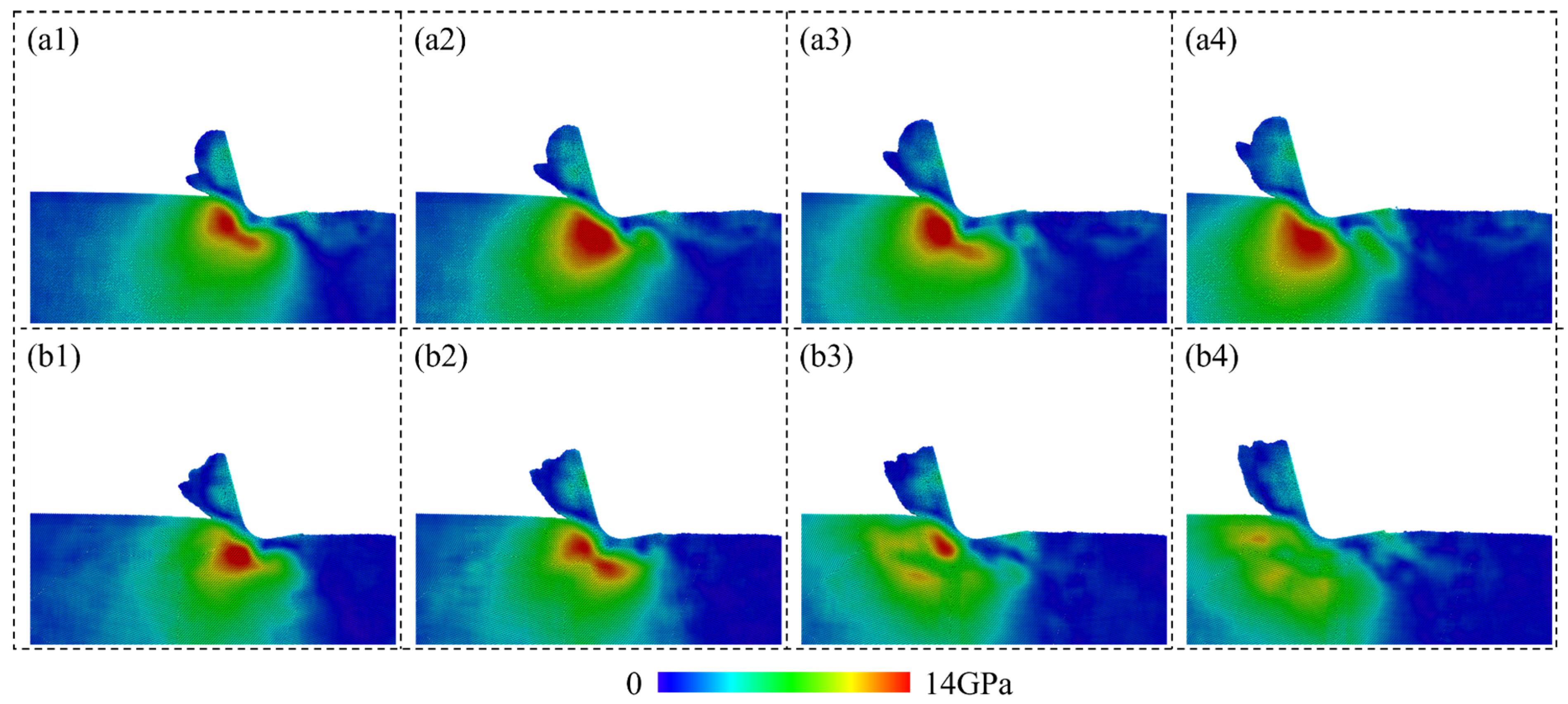
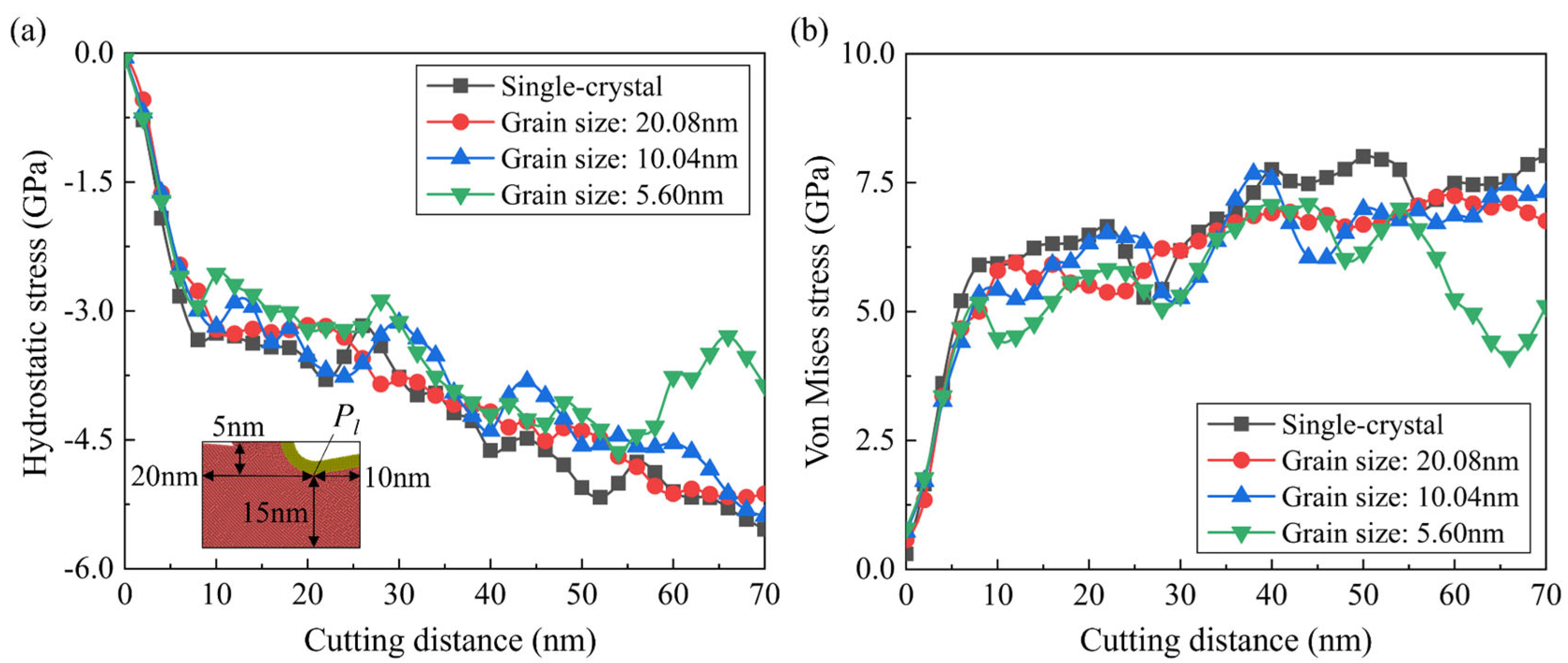
3.2.3. Internal Stress and Temperature
4. Conclusions
- In nanometric cutting, the stagnation region can be less apparent and more nanogrooves are generated at GBs when cutting on the polycrystal workpiece. As the grain size decreases, the material removal process becomes unstable and higher removal efficiency is achieved. Massive nanocrystals are generated in the workpiece due to the intra-granular facture and squeeze of the disordered atoms, while on the machined surface, the elastic recovery layer becomes irregular and pits are observed on the machined surface.
- When cutting on the polycrystal workpiece, the average frictional coefficient is higher than single crystals and increases as the grain size decreases. This variation is attributed to the decrease in nominal force, since the density of GBs tends to have a more apparent influence in releasing the downward compression than resistance of cutting tool motion.
- For a polycrystal workpiece, slip along the GBs merges as a nonnegligible process of the plastic deformation in workpiece. With the decrease in grain size, the elastic deformation ahead of the cutting tool can be less apparent as the strain energy is dissipated by enhanced slip motion. More 5-coordinated atoms are generated, especially when the grain size decreases, while fewer atoms with high coordination numbers (CN ≥ 6) are generated in the deformation region.
- When cutting on the polycrystal workpiece, the fluctuation in compressive stress and von Mises stress is more apparent and the workpiece temperature is higher than with a single-crystal workpiece. As the grain size decreases, the average stress decreases, since the GBs facilitate plastic deformation and release the strain energy while the average workpiece temperature increases due to the impediment of heat transfer by GBs.
Author Contributions
Funding
Data Availability Statement
Conflicts of Interest
References
- Ballif, C.; Haug, F.J.; Boccard, M.; Verlinden, P.J.; Hahn, G. Status and perspectives of crystalline silicon photovoltaics in research and industry. Nat. Rev. Mater. 2022, 7, 597–616. [Google Scholar] [CrossRef]
- Yan, J.; Asami, T.; Harada, H.; Kuriyagawa, T. Crystallographic effect on subsurface damage formation in silicon microcutting. CIRP Ann.-Manuf. Technol. 2012, 61, 131–134. [Google Scholar] [CrossRef]
- Wang, Z.; Zhang, J.; Lu, J. Effects of crystallographic orientations and grain boundaries on nanoscratching behaviour of unique bi-crystal Cu. Wear 2022, 498–499, 204313. [Google Scholar] [CrossRef]
- Chen, J.; Ding, F.; Luo, X.; Rao, X.; Sun, J. Fundamental study of ductile-regime diamond turning of single crystal gallium arsenide. Precis. Eng. 2020, 62, 71–82. [Google Scholar] [CrossRef]
- Li, A.; Szlufarska, I. How grain size controls friction and wear in nanocrystalline metals. Phys. Rev. B 2015, 92, 075418. [Google Scholar] [CrossRef]
- Fung, K.Y.; Tang, C.Y.; Cheung, C.F. Molecular dynamics analysis of the effect of surface flaws of diamond tools on tool wear in nanometric cutting. Comput. Mater. Sci. 2017, 133, 60–70. [Google Scholar] [CrossRef]
- Alhafez, I.A.; Urbassek, H.M. Scratching of hcp metals: A molecular-dynamics study. Comput. Mater. Sci. 2016, 113, 187–197. [Google Scholar] [CrossRef]
- Mylvaganam, K.; Zhang, L.C. Nanotwinning in monocrystalline silicon upon nanoscratching. Scr. Mater. 2011, 65, 214–216. [Google Scholar] [CrossRef]
- Chavoshi, S.Z.; Xu, S.; Luo, X. Dislocation-mediated plasticity in silicon during nanometric cutting: A molecular dynamics simulation study. Mater. Sci. Semicond. Process. 2016, 51, 60–70. [Google Scholar] [CrossRef]
- Liu, C.; Chen, X.; Ke, J.; She, Z.; Zhang, J.; Xiao, J.; Xu, J. Numerical investigation on subsurface damage in nanometric cutting of single-crystal silicon at elevated temperatures. J. Manuf. Process. 2021, 68, 1060–1071. [Google Scholar] [CrossRef]
- Fang, F.; Wu, H.; Liu, Y. Modelling and experimental investigation on nanometric cutting of monocrystalline silicon. Int. J. Mach. Tools Manuf. 2005, 45, 1681–1686. [Google Scholar] [CrossRef]
- Wang, J.; Zhang, X.; Fang, F.; Chen, R. A numerical study on the material removal and phase transformation in the nanometric cutting of silicon. Appl. Surf. Sci. 2018, 455, 608–615. [Google Scholar] [CrossRef]
- Lai, M.; Zhang, X.; Fang, F. Crystal Orientation Effect on the Subsurface Deformation of Monocrystalline Germanium in Nanometric Cutting. Nanoscale Res. Lett. 2017, 12, 296. [Google Scholar] [CrossRef] [PubMed]
- Lai, M.; Zhang, X.; Fang, F.; Bi, M. Fundamental investigation on partially overlapped nano-cutting of monocrystalline germanium. Precis. Eng. 2017, 49, 160–168. [Google Scholar] [CrossRef]
- Goel, S.; Stukowski, A.; Luo, X.; Agrawal, A.; Reuben, R.L. Anisotropy of single-crystal 3C–SiC during nanometric cutting. Model. Simul. Mater. Sci. Eng. 2013, 21, 065004. [Google Scholar] [CrossRef]
- Meng, B.; Yuan, D.; Xu, S. Study on strain rate and heat effect on the removal mechanism of SiC during nano-scratching process by molecular dynamics simulation. Int. J. Mech. Sci. 2019, 151, 724–732. [Google Scholar] [CrossRef]
- Zhou, P.; Sun, T.; Shi, X.; Li, J.; Zhu, Y.; Wang, Z. Atomic-scale study of vacancy defects in SiC affecting on removal mechanisms during nano-abrasion process. Tribol. Int. 2020, 145, 106136. [Google Scholar] [CrossRef]
- Tian, Z.; Xu, X.; Jiang, F.; Lu, J.; Luo, Q.; Lin, J. Study on nanomechanical properties of 4H-SiC and 6H-SiC by molecular dynamics simulations. Ceram. Int. 2019, 45, 21998–22006. [Google Scholar] [CrossRef]
- Zhao, P.; Wu, J.; Chen, H.; Liu, H.; Li, D.; Tan, J. Molecular dynamics simulation study of interaction mechanism between grain boundaries and subgrain boundaries in nano-cutting. J. Manuf. Process. 2021, 67, 418–426. [Google Scholar] [CrossRef]
- Fan, P.; Goel, S.; Luo, X.; Yan, Y.; Geng, Y.; He, Y. Origins of ductile plasticity in a polycrystalline gallium arsenide during scratching: MD simulation study. Appl. Surf. Sci. 2021, 552, 149489. [Google Scholar] [CrossRef]
- Liu, Y.; Li, B.; Kong, L. Molecular dynamics simulation of silicon carbide nanoscale material removal behavior. Ceram. Int. 2018, 44, 11910–11913. [Google Scholar] [CrossRef]
- Zhao, L.; Hu, W.; Zhang, Q.; Zhang, J.; Zhang, J.; Sun, T. Atomistic origin of brittle-to-ductile transition behavior of polycrystalline 3C–SiC in diamond cutting. Ceram. Int. 2021, 47, 23895–23904. [Google Scholar] [CrossRef]
- Goel, S.; Kovalchenko, A.; Stukowski, A.; Cross, G. Influence of microstructure on the cutting behaviour of silicon. Acta Mater. 2016, 105, 464–478. [Google Scholar] [CrossRef]
- Liu, C.; Xu, W.; Zhang, J.; Xiao, J.; Chen, X.; Xu, J. Numerical investigation on the temperature effect in nanometric cutting of polycrystalline silicon. Int. J. Mech. Sci. 2022, 220, 107172. [Google Scholar] [CrossRef]
- Plimpton, S. Fast parallel algorithms for short-range molecular dynamics. J. Comput. Phys. 1995, 117, 1–19. [Google Scholar] [CrossRef]
- Stukowski, A. Visualization and analysis of atomistic simulation data with OVITO–the Open Visualization Tool. Model. Simul. Mater. Sci. Eng. 2010, 18, 015012. [Google Scholar] [CrossRef]
- Maras, E.; Trushin, O.; Stukowski, A.; Ala-Nissila, T.; Jónsson, H. Global transition path search for dislocation formation in Ge on Si(001). Comput. Phys. Commun. 2016, 205, 13–21. [Google Scholar] [CrossRef]
- Hirel, P. Atomsk: A tool for manipulating and converting atomic data files. Comput. Phys. Commun. 2015, 197, 212–219. [Google Scholar] [CrossRef]
- Voronoi, G. Nouvelles applications des paramètres continus à la théorie des formes quadratiques. Deuxième mémoire. Recherches sur les parallélloèdres primitifs. J. Reine Angew. Math. (Crelles J.) 1908, 1908, 198–287. [Google Scholar] [CrossRef]
- Dirichlet, G.L. Über die Reduction der positiven quadratischen Formen mit drei unbestimmten ganzen Zahlen. J. Reine Angew. Math. (Crelles J.) 1850, 1850, 209–227. [Google Scholar]
- Goel, S.; Luo, X.; Agrawal, A.; Reuben, R.L. Diamond machining of silicon: A review of advances in molecular dynamics simulation. Int. J. Mach. Tools Manuf. 2015, 88, 131–164. [Google Scholar] [CrossRef]
- Erhart, P.; Albe, K. Analytical potential for atomistic simulations of silicon, carbon, and silicon carbide. Phys. Rev. B 2005, 71, 035211. [Google Scholar] [CrossRef]
- Goel, S.; Luo, X.; Reuben, R.L.; Pen, H. Influence of temperature and crystal orientation on tool wear during single point diamond turning of silicon. Wear 2012, 284–285, 65–72. [Google Scholar] [CrossRef]
- Meng, B.; Yuan, D.; Zheng, J.; Qiu, P.; Xu, S. Tip-based nanomanufacturing process of single crystal SiC: Ductile deformation mechanism and process optimization. Appl. Surf. Sci. 2020, 500, 144039. [Google Scholar] [CrossRef]
- Guo, X.; Li, Q.; Liu, T.; Zhai, C.; Kang, R.; Jin, Z. Molecular dynamics study on the thickness of damage layer in multiple grinding of monocrystalline silicon. Mater. Sci. Semicond. Process. 2016, 51, 15–19. [Google Scholar] [CrossRef]
- Cheong, W.C.D.; Zhang, L.C. Molecular dynamics simulation of phase transformations in silicon monocrystals due to nano-indentation. Nanotechnology 2000, 11, 173–180. [Google Scholar] [CrossRef]
- Cai, M.B.; Li, X.P.; Rahman, M. Characteristics of “dynamic hard particles” in nanoscale ductile mode cutting of monocrystalline silicon with diamond tools in relation to tool groove wear. Wear 2007, 263, 1459–1466. [Google Scholar] [CrossRef]
- Zhao, L.; Zhang, J.; Zhang, J.; Hartmaier, A. Atomistic investigation of machinability of monocrystalline 3C–SiC in elliptical vibration-assisted diamond cutting. Ceram. Int. 2021, 47, 2358–2366. [Google Scholar] [CrossRef]
- Yan, J.; Asami, T.; Harada, H.; Kuriyagawa, T. Fundamental investigation of subsurface damage in single crystalline silicon caused by diamond machining. Precis. Eng. 2009, 33, 378–386. [Google Scholar] [CrossRef]
- Dai, H.; Zhang, F.; Zhou, Y. Numerical study of three-body diamond abrasive polishing single crystal Si under graphene lubrication by molecular dynamics simulation. Comput. Mater. Sci. 2020, 171, 109214. [Google Scholar] [CrossRef]
- Liu, C.; Zhang, J.; Zhang, J.; Chen, X.; Xiao, J.; Xu, J. A simulation investigation on elliptical vibration cutting of single-crystal silicon. Int. J. Adv. Manuf. Technol. 2020, 108, 2231–2243. [Google Scholar] [CrossRef]
- Stukowski, A. Computational Analysis Methods in Atomistic Modeling of Crystals. JOM 2014, 66, 399–407. [Google Scholar] [CrossRef]
- Yan, Y.; Li, Z.; Jia, J.; Wang, J.; Geng, Y. Molecular dynamics simulation of the combination effect of the tip inclination and scratching direction on nanomachining of single crystal silicon. Comput. Mater. Sci. 2021, 186, 110014. [Google Scholar] [CrossRef]
- Khatri, N.; Barkachary, B.M.; Muneeswaran, B.; Al-Sayegh, R.; Luo, X.; Goel, S. Surface defects incorporated diamond machining of silicon. Int. J. Extrem. Manuf. 2020, 2, 045102. [Google Scholar] [CrossRef]
- Dai, H.; Zhou, Y.; Zhang, F. Atomistic simulation of influence of laser nano-structured diamond abrasive on the polishing behavior of silicon. Mater. Sci. Semicond. Process. 2020, 105, 104706. [Google Scholar] [CrossRef]


| Properties | Parameters |
|---|---|
| Size of workpiece (x × y × z) | 100.0 nm × 5.4 nm × 44.5 nm |
| Rake/flank angle of cutting tool | −10°/10° |
| Total number of atoms | About 1.33–1.34 million |
| Cutting temperature | 300 K |
| Material removal thickness | 5 nm |
| Radius of tool edge | 5 nm |
| Cutting speed | 20 m/s |
Disclaimer/Publisher’s Note: The statements, opinions and data contained in all publications are solely those of the individual author(s) and contributor(s) and not of MDPI and/or the editor(s). MDPI and/or the editor(s) disclaim responsibility for any injury to people or property resulting from any ideas, methods, instructions or products referred to in the content. |
© 2024 by the authors. Licensee MDPI, Basel, Switzerland. This article is an open access article distributed under the terms and conditions of the Creative Commons Attribution (CC BY) license (https://creativecommons.org/licenses/by/4.0/).
Share and Cite
Guo, W.; Yu, Q.; Wang, G.; Fu, S.; Liu, C.; Chen, X. Effect of Grain Size on Nanometric Cutting of Polycrystalline Silicon via Molecular Dynamics Simulation. Micromachines 2024, 15, 767. https://doi.org/10.3390/mi15060767
Guo W, Yu Q, Wang G, Fu S, Liu C, Chen X. Effect of Grain Size on Nanometric Cutting of Polycrystalline Silicon via Molecular Dynamics Simulation. Micromachines. 2024; 15(6):767. https://doi.org/10.3390/mi15060767
Chicago/Turabian StyleGuo, Wen, Qiuyue Yu, Guoyan Wang, Shuming Fu, Changlin Liu, and Xiao Chen. 2024. "Effect of Grain Size on Nanometric Cutting of Polycrystalline Silicon via Molecular Dynamics Simulation" Micromachines 15, no. 6: 767. https://doi.org/10.3390/mi15060767