Article

Density Functional Theory Provides Insights into β-SnSe Monolayers as a Highly Sensitive and Recoverable Ozone Sensing Material

1
Department of Engineering Technology, Guangdong Open University, Guangzhou 510091, China
2
Centre for Optical and Electromagnetic Research, South China Academy of Advanced Optoelectronics, South China Normal University, Guangzhou 510006, China
3
Ministry of Education Key Laboratory of Textile Fiber Products, School of Materials Science and Engineering, Wuhan Textile University, Wuhan 430220, China
4
School of Materials and Chemistry Engineering, Tongren University, Tongren 554300, China
5
School of Artificial Intelligence, Guangdong Vocational College of Post and Telecom, Guangzhou 510630, China
6
Big Data Engineering College, Kaili University, Kaili 556011, China
*
Authors to whom correspondence should be addressed.
Micromachines 2024, 15(8), 960; https://doi.org/10.3390/mi15080960
Submission received: 25 June 2024 / Revised: 21 July 2024 / Accepted: 24 July 2024 / Published: 27 July 2024
(This article belongs to the Special Issue Gas Sensors: From Fundamental Research to Applications)

Abstract

:
This study explores the potential of β-SnSe monolayers as a promising material for ozone (O3) sensing using density functional theory (DFT) combined with the non-equilibrium Green’s function (NEGF) method. The adsorption characteristics of O3 molecules on the β-SnSe monolayer surface were thoroughly investigated, including adsorption energy, band structure, density of states (DOSs), differential charge density, and Bader charge analysis. Post-adsorption, hybridization energy levels were introduced into the system, leading to a reduced band gap and increased electrical conductivity. A robust charge exchange between O3 and the β-SnSe monolayer was observed, indicative of chemisorption. Recovery time calculations also revealed that the β-SnSe monolayer could be reused after O3 adsorption. The sensitivity of the β-SnSe monolayer to O3 was quantitatively evaluated through current-voltage characteristic simulations, revealing an extraordinary sensitivity of 1817.57% at a bias voltage of 1.2 V. This sensitivity surpasses that of other two-dimensional materials such as graphene oxide. This comprehensive investigation demonstrates the exceptional potential of β-SnSe monolayers as a highly sensitive, recoverable, and environmentally friendly O3 sensing material.

1. Introduction

Ozone (O3), as a trace gas in the atmosphere, possesses a strong oxidizing capacity that can irritate the respiratory tract and eyes, especially affecting children, the elderly, and those with respiratory diseases. When present above certain levels, ozone can adversely impact physical and mental health. Monitoring ozone levels is crucial for maintaining its relative stability in the atmosphere and ensuring air quality.
Currently, ozone monitoring primarily relies on two methods: spectrophotometry and chemiluminescence. The former utilizes ultraviolet characteristics to measure ozone concentration based on absorption and wavelength in a medium, while the latter determines concentration based on the intensity of emitted light. However, both methods require laboratory settings, are time-consuming, and incur high costs, making continuous real-time monitoring of ozone levels challenging.
Nanostructured materials have emerged as promising candidates for ozone sensing due to their inherent advantages. Their high surface-to-volume ratio facilitates enhanced gas–solid interactions, promoting efficient ozone adsorption and subsequent sensing mechanisms. One-dimensional nanotubes, exemplified by pristine single-walled aluminum nitride nanotubes [1], and zero-dimensional nanocages, including Ni-doped Zn12O12 [2], B12N12 [3], BN fullerene-like structures [4], AlB11N12, GaB11N12, and Al12N12 [5], have shown particular promise for ozone detection. These nanostructures possess hollow interiors and abundant unsaturated surface atoms, both of which contribute to their ozone sensing capabilities.
Leveraging the excellent adsorptive properties of TiO2, nanomaterials based on TiO2, such as quantum dots of TiO2 [6], N-doped TiO2-supported Au nanocomposites [7], TiO2/WSe2 heterostructures [8], and nitrogen-doped TiO2/ZnO, have been employed to augment ozone adsorption. Additionally, the ozone sensing performance of graphene-based two-dimensional materials, including B-doped graphene [9], Pt-decorated graphene [10], and graphene oxide [11], has been studied.
In addition to these burgeoning two-dimensional materials, tin-based materials have garnered significant attention for their potential in ozone sensing applications. Boron doping has been shown to enhance charge transfer from stanene to ozone molecules, positioning it as a promising candidate for the development of sensitive ozone sensors [12]. Furthermore, the formation of heterojunctions, particularly by integrating stanene with materials like TiO2, has been investigated to exploit synergistic effects that further amplify ozone sensing performance [13]. These advancements underscore the innovative strides being made in the realm of material science for environmental monitoring. Furthermore, SnS has been identified as exhibiting a high degree of efficacy in interacting with ozone, positioning it as a promising candidate for chemical sensing in ozone detection methodologies [14].
β-SnSe (hereafter referred to as SnSe), a layered transition metal chalcogenide with a graphene-analogous structure, has attracted considerable interest owing to its extraordinary attributes and diverse potential applications. At elevated temperatures, SnSe exhibits an exceptionally low lattice thermal conductivity, rendering it a promising material for thermoelectric energy conversion [15,16,17]. Notably, SnSe possesses desirable characteristics, including chemical stability, non-toxicity, and abundant terrestrial reserves, making it suitable for large-scale applications and sustainable development. SnSe possesses a tunable band gap and superior light absorption properties, particularly in its monolayer form, where it demonstrates significant photoresponsiveness and exceptional photoelectric performance [18]. In terms of gas sensing, SnSe has demonstrated strong chemical adsorption towards various gas molecules, such as methanol (CH3OH), oxygen (O2), nitrogen dioxide (NO2), and sulfur dioxide (SO2), making it a compelling candidate for gas detection applications [19].
In this study, the potential performance of monolayer SnSe as an O3 sensing material was systematically investigated using density functional theory (DFT) combined with the non-equilibrium Green’s function (NEGF) method. Theoretical calculations provided an in-depth analysis of the adsorption characteristics of O3 molecules on the surface of monolayer SnSe, involving adsorption energy, band structure, density of states (DOSs), differential charge density, and Bader charge analysis. These calculations revealed the interaction mechanism and electron transfer process between the monolayer SnSe and O3 molecules, elucidating its fundamental sensing properties as an O3 gas detector. Additionally, this work specifically considered the recoverability of monolayer SnSe in practical applications, evaluating the recovery time after O3 adsorption through computational assessments. Furthermore, the response sensitivity of monolayer SnSe to O3 gas was quantitatively explored based on current-voltage (I–V) characteristic simulations. This research demonstrates the immense potential of monolayer SnSe as a highly sensitive, recoverable, and environmentally friendly O3 sensing material.

2. Materials and Methods

First-principle calculations were performed using the Vienna Ab initio Simulation Package (VASP) 5.4 within the framework of DFT [20,21]. The exchange-correlation energy was treated with the generalized gradient approximation (GGA) in the form of the Perdew–Burke–Ernzerhof (PBE) functional [22]. To accurately account for the potential weak interactions, such as van der Waals forces, between the molecules and the substrate, the DFT-D3 correction scheme was further employed [23]. Spin polarization effects were also considered in the calculations.
Specifically, a 4 × 4 supercell system comprising 64 atoms was constructed to simulate the two-dimensional structure of an SnSe monolayer. An energy cutoff of 400 eV was set to ensure calculation accuracy. During the structural optimization, the maximum force on each atom was required to be lower than 0.02 eV/Å, and the total energy convergence criterion was also set to 10−5 eV to ensure sufficient accuracy in the structural optimization. Considering the effects of periodic boundary conditions, a 20 Å vacuum layer was established in the perpendicular direction to prevent interactions between adjacent periods. For Brillouin zone sampling, a Monkhorst–Pack grid of 4 × 4 × 1 was utilized.
The adsorption energy (Ead) of the O3 molecule on the SnSe monolayer surface was calculated using the following equation:
E a d = E t o t a l E S n S e E O 3
where Etotal is the total adsorption energy of the optimized systems after O3 adsorption on the SnSe monolayer, ESnSe is the energy of the optimized pristine SnSe monolayer, and EO3 denotes the energy of the O3 molecule involved.
The current-voltage characteristics (I–V curves) were conducted using the tranSiesta module within the Siesta 4.1.5 software package, in conjunction with NEGF theory [24]. Utilizing the Landauer–Büttiker formula [25], the electrical currents across the material under varying voltages were determined:
I V b = 2 e h μ R μ L T E , V b f E μ L f E μ R
Here, I signify the electric current traversing the contact electrode at the bias voltage (Vb). The terms μL and μR represent the electrochemical potentials of the left and right electrodes, respectively. T E , V b denotes the transmission coefficient at voltage Vb and energy E. The f E μ L accounts for the Fermi–Dirac distribution function of the left and right electrodes at energy E.
Additionally, the VESTA 3.90.0a software was used to analyze the differential charge density distribution of the system before and after adsorption, as well as the optimized geometric configuration [26]. Finally, the vaspkit 1.3.3 tool was employed for effective post-processing and analysis of the raw computational data [27].

3. Results and Discussion

3.1. Structures

As depicted in Figure 1, the SnSe monolayer comprises two facets: the tin (Sn) side and the selenium (Se) side. On the Sn side, the O3 molecule may occupy four potential sites: atop the Sn atom (TSn1), atop the Se atom (Tse1), on the hollow site (H1), or on the bridge site (B1) between Sn and Se bonds. Similarly, on the Se side, the O3 molecule may be located atop the Sn atom (Tsn2), atop the Se atom (Tse2), on the hollow site (H2), or on the bridge site (B2) between Sn and Se bonds. Upon adsorption to the surface, the O3 molecule may approach in various orientations: with the lateral oxygen atoms near the surface and the central oxygen atom farther away, with a perpendicular arrangement to the SnSe surface; with the central oxygen atom near the surface and the lateral oxygen atoms farther away, with a perpendicular arrangement to the SnSe surface; or with the plane formed by the three oxygen atoms parallel to the SnSe surface. Energy calculations for different configurations indicate that the most stable and energetically favorable configuration is where the O3 molecule bridges between the Sn and Se bonds, with the lateral oxygen atoms approaching the surface and the central oxygen atom remaining farther away, forming a perpendicular orientation to the Sn side of the SnSe surface.
As plotted in Figure 2a, the O3 molecule induces significant reconstruction of the SnSe monolayer surface during the adsorption process. Before adsorption, the Sn-Se bond length is approximately 2.744 Å, with a bond angle of 90.741°. However, upon O3 adsorption, the Sn atom beneath the adsorption site experiences a strong attractive force from the oxygen atoms, causing it to move closer to the oxygen atoms. This results in a contraction of the Sn-Se bond length to 2.657 Å, while the bond length between the Sn atom and the adjacent Se atoms elongates to 2.769 Å. Consequently, the Sn-Se-Se bond angle expands to 97.417°, reflecting the substantial impact of O3 adsorption on the SnSe surface structure. In the adsorption configuration, the distance between the closest oxygen atom of the O3 molecule and the Sn surface is 2.251 Å, suggesting the possibility of a strong adsorption interaction between Sn and the O3 molecule.
The calculated adsorption energy of the O3 molecule on the SnSe monolayer is −1.826 eV. This negative value clearly indicates that the O3 molecule adsorption on the SnSe surface is a thermodynamically spontaneous process that can proceed without the input of additional external energy. In other words, SnSe exhibits a strong affinity and easy adsorption for O3 molecules and can effectively capture O3 molecules at room temperature. Therefore, it is a promising candidate material for room-temperature O3 gas sensors.

3.2. Electronic Properties

In the in-depth exploration of the intrinsic mechanism behind the O3 gas sensing performance of monolayer SnSe, computational analysis was conducted on the electronic structure and band characteristics of monolayer SnSe before and after O3 adsorption. The Fermi level is adjusted to the zero point, and the band structure near the Fermi level, which is crucial for semiconductor properties, is specifically presented within the energy range of −4 eV to 4 eV.
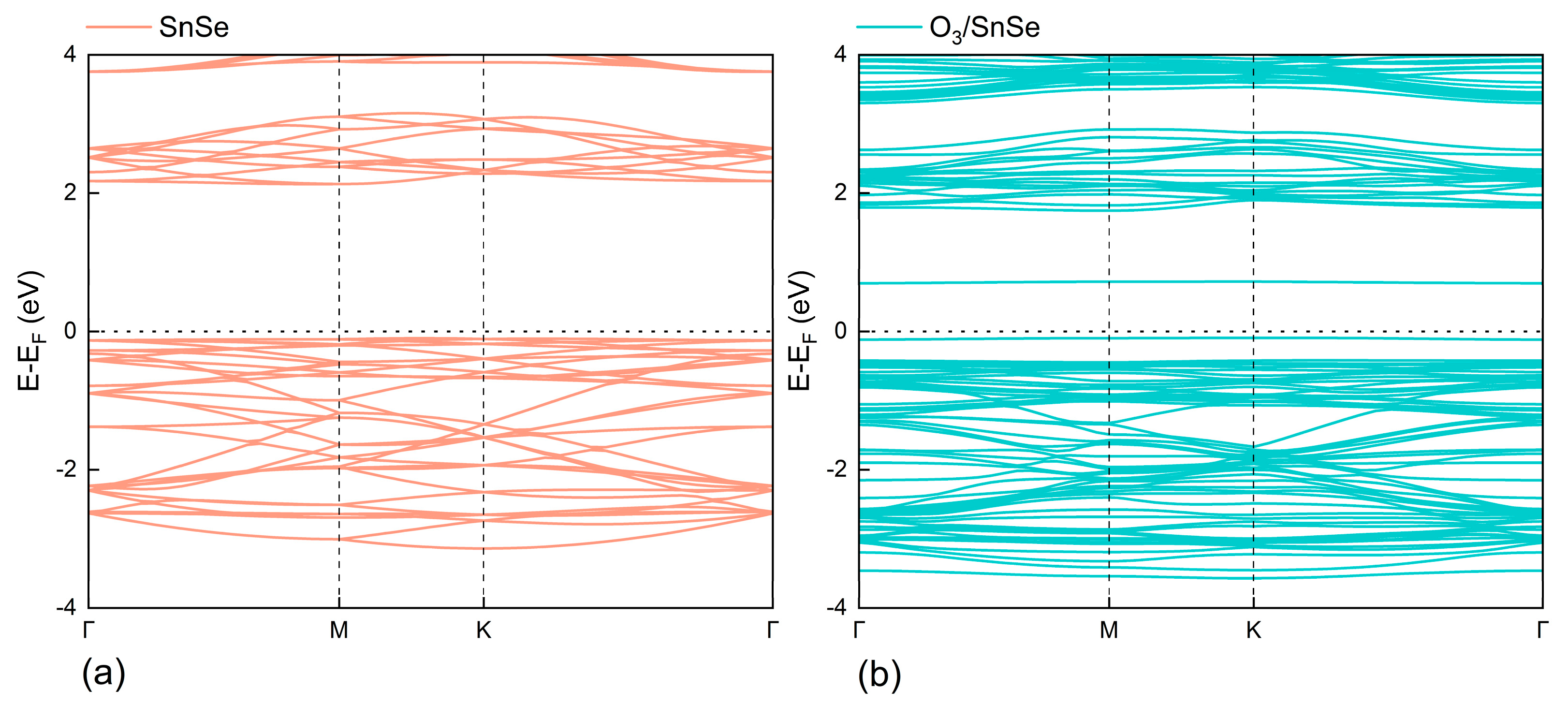
The pristine SnSe monolayer is calculated to exhibit a theoretical band gap of 2.228 eV, as illustrated in Figure 3a, which is in close agreement with the previously reported theoretical value of 2.22 eV [16]. Upon O3 molecule adsorption on the SnSe monolayer surface, its electronic structure undergoes significant reconstruction. The adsorption process introduces new impurity energy levels near the Fermi level, which originate from the valence band maximum (VBM) and conduction band minimum (CBM) of the SnSe monolayer. These impurity energy levels directly influence the original band structure of SnSe, as seen in Figure 3b, leading to a remarkable decrease in the band gap to 0.790 eV.
This significant band gap narrowing implies that the conductivity of the SnSe monolayer is greatly enhanced after O3 adsorption. The newly formed impurity energy levels allow electrons in the valence band to jump to the conduction band at a lower energy threshold. Compared to the state before O3 adsorption, the activation energy required for electron migration is significantly reduced. Such changes in the electronic structure greatly improve the sensitive response efficiency of the SnSe monolayer to external stimuli as an O3 gas sensor.
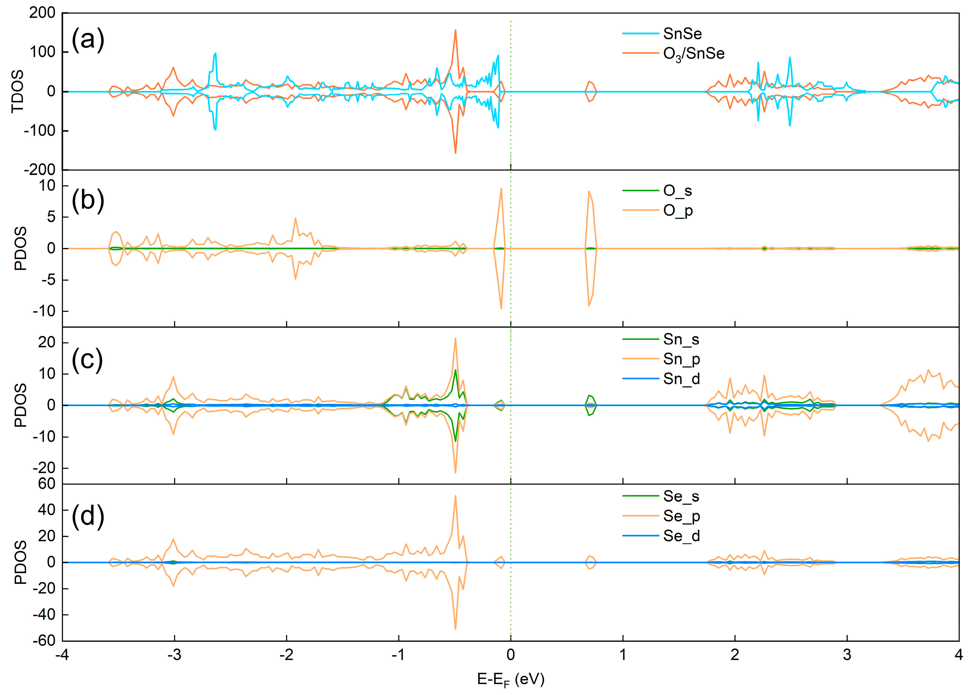
Figure 4 delineates the total density of states (TDOSs) and partial density of states (PDOSs), where the adsorption of O3 on SnSe introduces hybridization energy levels flanking the Fermi level. The TDOSs analysis reveals a pronounced symmetry in the DOS curves for both spin-up and spin-down configurations, indicating the non-magnetic nature of the adsorption structure. Notably, significant peaks at energy values of −0.085 eV and 0.697 eV are observed, predominantly originating from the p orbitals of oxygen atoms.
At −0.085 eV, the oxygen-dominated absorption peak triggers peak responses in the s and p orbitals of Sn atoms and the p orbitals of Se atoms at the same energy level, unveiling a robust orbital hybridization indicative of changes in electron cloud distribution and energy level rearrangement during adsorption. Similarly, at 0.697 eV, oxygen atoms induce corresponding peaks in the s orbitals of Sn atoms and the p orbitals of Se atoms. These enhancements in electron density at specific energy levels directly affect the material’s band structure, particularly introducing impurity levels near the top of the valence band and altering the electronic transport characteristics near the bottom of the conduction band, thereby modifying the material’s electrical conductivity and reactive properties post-adsorption.
To elucidate the bonding characteristics of adsorbed atoms on the SnSe monolayer surface, the charge density differential was computed using the following equation:
ρ = ρ S n S e + O 3 ρ S n S e ρ O 3
where Δρ represents the charge density differential, ρSnSe+O3 is the charge density of the adsorption system, ρSnSe is the charge density of the SnSe monolayer surface, and ρO3 is the charge density of the adsorbed O3 molecule.
Figure 2b presents three-dimensional isosurface plots of the differential charge density, where yellow regions represent electron accumulation and blue regions represent electron depletion. As seen in Figure 2b, when the O3 molecule is adsorbed on the SnSe monolayer surface, a significant electron depletion region appears on the Sn atom side opposite to the O atom, while a large amount of electron accumulation occurs around the O atom. This indicates that the O atom gains electrons from the Sn atom. Additionally, Figure 2b also reveals that the surface of the three Se atoms bonded to the O3 molecule also exhibits electron depletion regions, further confirming the transfer of electrons from the SnSe monolayer to the O3 molecule during the adsorption process.
Bader charge analysis reveals that the O3 molecule gains a net charge of 0.881 electron units, while the bonded Sn atom loses 1.200 electron units. This result provides strong evidence for a significant charge exchange phenomenon occurring between the O3 molecule and the SnSe surface, suggesting the high adsorption stability of the O3 molecule on the SnSe surface.

3.3. Recovery Time

Recovery time is a critical metric for evaluating the reversibility of sensors, referring to the time required to desorb target gas molecules from the surface of the sensing material. Recovery time τ is typically inversely related to adsorption energy and can be estimated through transition state theory:
τ = e x p E a d k B T / ω
where Ead is the adsorption energy, kB is the Boltzmann constant, and T is the temperature. ω is the attempt frequency, assumed to be 1013 s−1 [28].
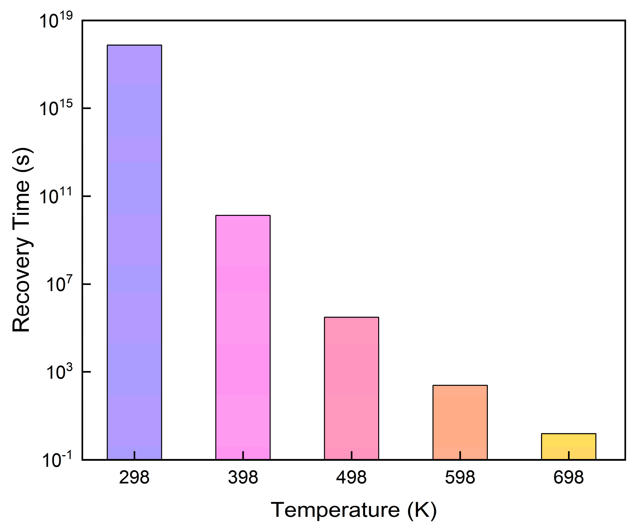
Figure 5 illustrates how temperature affects the recovery time of the SnSe monolayer following O3 molecule adsorption. The recovery time for the SnSe monolayer following O3 adsorption can reach 7.61 × 10¹⁷ s at an ambient temperature of 298 K. This finding underscores the exceptional O3 adsorption potential of SnSe even at room temperature. The O3 molecules’ desorption time, however, drastically decreases to 244.91 s as the temperature steadily rises to 598 K. At a temperature of 698 K, the recovery time is observed to be 1.53 s. This observation implies that at higher temperatures, the adsorption of O3 on the SnSe monolayer becomes more reversible, enabling a rapid recovery to the initial state and demonstrating excellent dynamic response performance.

3.4. Sensitivity

To gain insight into the sensing capabilities of SnSe towards ozone, the sensitivity (S) of SnSe is calculated using the following equation:
S = I I 0 / I 0
where I and I0 are the currents across the scattering region when adsorbed with O3 and in their pristine condition, respectively.
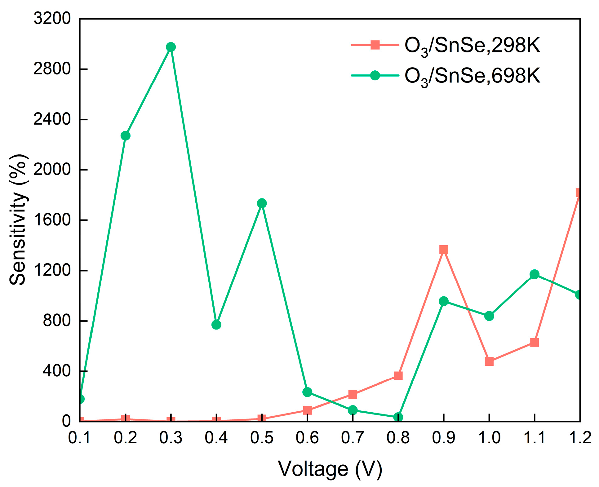
An examination of the current-voltage (I–V) characteristics appears in Figure 6, which clarifies that O3 adsorption has very little effect on the semiconductor surface current at lower bias voltage ranges (≤0.6 V). This finding points to a slight difference in current values between the O3 adsorption and non-adsorption states. This suggests that at low voltage driving, O3 adsorption does not significantly alter the carrier transport characteristics of the semiconductor interface. Substituting the calculated current values into Equation (5) yields the sensitivity-voltage curve. As depicted in Figure 7, the sensitivity-voltage curve of SnSe for O3 at room temperature indicates that within the 0–0.6 V range, the sensitivity of SnSe to O3 detection remains relatively low and is consistently below 100%.
However, within the bias voltage range of 0.7 to 1.2 V, the influence of adsorbed O3 molecules on the surface current becomes more pronounced, resulting in SnSe exhibiting a sensitivity to O3 exceeding 200%. At a bias voltage of 1.2 V, the current response of the O3-adsorbed surface exhibits a marked enhancement, reaching a value of 2.54 × 10⁻⁶ μA. This represents an approximately one-order-of-magnitude increase compared to the current measured for the unadsorbed surface (1.33 × 10⁻⁷ μA), indicating a high degree of sensitivity. Consequently, the sensor system exhibits a remarkable sensitivity of 1817.57% at a working voltage of 1.2 V. This strongly proves that under high voltage excitation, the interaction between O3 and the semiconductor interface will greatly promote charge transfer and induce significant resistance changes, thus enabling the SnSe monolayer to have a highly sensitive detection capability for O3 molecules.
To comprehensively assess the detection capability of SnSe for O3 across different temperatures, the impact of temperature variations on the current-voltage (I–V) characteristics and sensitivity was investigated. The I–V curves at 298 K and 698 K are presented in Figure S1. As illustrated in Figure S1, increasing the temperature from 298 K to 698 K results in a significant rise in the current of SnSe post-O3 adsorption within the low bias voltage range (0–0.6 V), markedly surpassing the current of SnSe without O3 adsorption. Additionally, at 0.9–1.2 V, the current of SnSe post-O3 adsorption is distinctly higher than that of SnSe without O3 adsorption. Figure 7 illustrates that SnSe exhibits a sensitivity to O3 exceeding 200% at bias voltages of 0.2–0.6 V and 0.9–1.2 V. This observation suggests that, at elevated temperatures, the operational voltage range for O3 detection by SnSe extends to the lower voltage range of 0.2–0.6 V.
In addition to considering the influence of operating temperature, the selectivity of sensors towards the target gas in the presence of interfering gases is crucial for practical applications. To assess the selectivity of SnSe for O3 detection, the I–V curves and sensitivities of SnSe upon exposure to O3 and common air gases (CO2 and O2) are compared in Figures S2 and S3. As shown in Figure S2, the current of CO2-adsorbed SnSe within the bias voltage range of 0.1–1.2 V is significantly lower than that of O3-adsorbed SnSe, indicating minimal interference from CO2 in O3 sensing. However, in the bias range of 0.1–0.7 V, the current of O2-adsorbed SnSe exceeds that of O3-adsorbed SnSe, leading to interference in O3 detection. Therefore, 0.1–0.7 V is not an optimal bias range for SnSe-based O3 sensing. At bias voltages greater than or equal to 0.8 V, the current of O3-adsorbed SnSe surpasses that of O2-adsorbed SnSe. The sensitivity curves in Figure S3 further demonstrate that within the bias range of 0.8–1.1 V, the sensitivity of O2-adsorbed SnSe remains below 90%, while the sensitivity of O3-adsorbed SnSe consistently exceeds 300%. At a bias voltage of 1.2 V, the sensitivity of O2-adsorbed SnSe increases to 262.15%, while the sensitivity for O3 detection is approximately 6.9 times higher, reaching 1817.57%, and far exceeding that of O2-adsorption. These results confirm that SnSe exhibits high selectivity for O3 detection in the presence of common air gases (O2 and CO2) within the bias range of 0.8–1.2 V.
From the analysis presented, it is evident that within the bias voltage range of 0.9–1.2 V, SnSe can detect O3 across various temperatures without interference from high concentrations of ambient gases. Consequently, SnSe shows promise as a highly selective, highly sensitive, and reusable material for O3 sensing.

3.5. Comparison

In this study, a comparative analysis of the SnSe monolayer with previously reported O3 nanosensors is conducted, as detailed in Supplementary Table S1. In terms of electron transfer, the charge transfer amounts when O3 interacts with stanene, B-doped stanene [12], BN fullerene-like nanocages [4], and Ni-decorated B12N12 nanocages [3] are 0.557 e, 0.548 e, 0.5 e, and 0.789 e, respectively. These values are all significantly lower than the 0.881 e charge transfer value observed at the O3-SnSe interface. Compared to other two-dimensional materials such as MoS2 [29] and SnS [14], SnSe exhibits an adsorption energy for O3 that is 5.1 times and 1.5 times greater, respectively. Additionally, the electron transfer amount for SnSe is 7.0 times and 1.1 times higher than that of MoS2 and SnS [14]. Our findings reveal that the interaction between SnSe and O3 is significantly stronger compared to other two-dimensional materials, while maintaining excellent reusability.
Notably, a greater chemical connection between the gas molecule and the surface is usually indicated by a larger charge transfer between SnSe and O3, which results in increased sensor sensitivity. Graphene oxide [11] has the highest documented sensitivity to O3 for two-dimensional materials at 860%. This work, however, reveals that SnSe has a sensitivity of 1817.57% to O3, which is almost 2.11 times higher than that of graphene oxide. This suggests that SnSe has the potential to be a highly sensitive O3 detector.

4. Conclusions

Our findings reveal that the SnSe monolayer exhibits remarkable potential as a high-performance O3 sensing material. The calculated adsorption energy of −1.826 eV indicates a strong and spontaneous adsorption of O3 molecules on the SnSe surface, suggesting efficient capture at room temperature. O3 adsorption significantly alters the electronic structure of the SnSe monolayer, inducing a substantial band gap narrowing from 2.228 eV to 0.790 eV. This phenomenon translates to a significant enhancement in electrical conductivity, which is a crucial factor for sensor response. Bader charge analysis confirms a substantial charge transfer of 0.881 electrons from the SnSe monolayer to the O3 molecule, signifying a strong interaction and high adsorption stability. The recovery time for O3 desorption from the SnSe monolayer is 244.91 s, demonstrating excellent dynamic response performance. Notably, the SnSe monolayer demonstrates an exceptional sensitivity of 1817.57% towards O3 gas at a working voltage of 1.2 V, surpassing the previously reported two-dimensional materials (graphene oxide, 860%). This superior sensitivity can be attributed to the strong charge transfer between SnSe and O3 molecules. In conclusion, the SnSe monolayer emerges as a promising candidate for the development of highly sensitive and environmentally friendly O3 sensors.

Supplementary Materials

The following supporting information can be downloaded at: https://www.mdpi.com/article/10.3390/mi15080960/s1, Figure S1. The sensitivity for intrinsic and O3-adsorbed SnSe monolayers at temperatures from 298 to 698 K. Figure S2. Current-voltage characteristics of SnSe monolayers without adsorbed gas molecules and with adsorbed O2, O3, and CO2. Figure S3. Voltage-dependent sensitivity curves of SnSe monolayers with adsorbed O2, O3, and CO2 molecules. Table S1. Comparison between this work with previous reports. References [1,3,4,11,12,14,29] are cited in the supplementary materials.

Author Contributions

Conceptualization, J.W. (Jiayin Wu); methodology, J.W. (Jiayin Wu); software, Z.L.; investigation, J.W. (Jiayin Wu); resources, T.L.; writing—original draft preparation, J.W. (Jiayin Wu); writing—review and editing, Q.M., T.L., J.W. (Jingting Wei) and B.L.; supervision, Z.L. and X.X.; funding acquisition, Q.M., T.L., Z.L. and B.L. All authors have read and agreed to the published version of the manuscript.

Funding

This research was funded by the Foundation Research Project of Kaili University, grant number 2022ZD05; National Natural Science Foundation of China, grant number 22269019; the Key Research Platform and Research Project of General Colleges and Universities in Guangdong Province, grant number 2022KTSCX289, 2023ZDZX1069; School-level Research Project of Guangdong Open University (Guangdong Polytechnic Institute), grant number ZD1905.

Data Availability Statement

The original contributions presented in the study are included in the article/Supplementary Materials, further inquiries can be directed to the corresponding authors.

Acknowledgments

The authors would like to thank Peiyuan Lai, Xianxu Li, Hongfei Qiu, Zhiqing Huang, and Pengchen Jian for their guidance on computational facilities.

Conflicts of Interest

The authors declare no conflicts of interest.

References

  1. Kamalinahad, S.; Solimannejad, M.; Shakerzadeh, E. Sensing of Ozone (O3) Molecule via Pristine Singe-Walled Aluminum Nitride Nanotube: A DFT Study. Superlattices Microstruct. 2016, 89, 390–397. [Google Scholar] [CrossRef]
  2. Munsif, S.; Ayub, K.; Nur-e-Alam, M.; Ahmed, S.; Ahmad, A.; Ul-Haq, Z. Sensing of H2S, NO2, SO2, and O3 through Pristine and Ni-Doped Zn12O12 Nanocage. Comput. Theor. Chem. 2023, 1229, 114305. [Google Scholar] [CrossRef]
  3. Rad, A.S.; Ayub, K. O3 and SO2 Sensing Concept on Extended Surface of B12N12 Nanocages Modified by Nickel Decoration: A Comprehensive DFT Study. Solid State Sci. 2017, 69, 22–30. [Google Scholar] [CrossRef]
  4. Panahyab, A.; Soleymanabadi, H. Ozone Adsorption on a BN Fullerene-like Nano-Cage: A DFT Study. Main Group Chem. 2016, 15, 347–354. [Google Scholar] [CrossRef]
  5. Roy, D.; Hossain, M.R.; Hossain, M.K.; Hossain, M.A.; Ahmed, F. Density Functional Theory Study of the Sensing of Ozone Gas Molecules by Using Fullerene-like Group-III Nitride Nanostructures. Phys. B Condens. Matter 2023, 650, 414553. [Google Scholar] [CrossRef]
  6. Abd-Elkader, O.H.; Sakr, M.A.S.; Saad, M.A.; Abdelsalam, H.; Zhang, Q. Electronic and Gas Sensing Properties of Ultrathin TiO2 Quantum Dots: A First-Principles Study. Results Phys. 2023, 52, 106804. [Google Scholar] [CrossRef]
  7. Abbasi, A.; Sardroodi, J.J. Application of TiO2-Supported Au for Ozone Molecule Removal from Environment: A van Der Waals-Corrected DFT Study. Int. J. Environ. Sci. Technol. 2019, 16, 3483–3496. [Google Scholar] [CrossRef]
  8. Abbasi, A.; Sardroodi, J.J. Investigation of the Adsorption of Ozone Molecules on TiO2/WSe2 Nanocomposites by DFT Computations: Applications to Gas Sensor Devices. Appl. Surf. Sci. 2018, 436, 27–41. [Google Scholar] [CrossRef]
  9. Rad, A.S.; Shabestari, S.S.; Mohseni, S.; Aghouzi, S.A. Study on the Adsorption Properties of O3, SO2, and SO3 on B-Doped Graphene Using DFT Calculations. J. Solid State Chem. 2016, 237, 204–210. [Google Scholar] [CrossRef]
  10. Shokuhi Rad, A.; Zareyee, D. Adsorption Properties of SO2 and O3 Molecules on Pt-Decorated Graphene: A Theoretical Study. Vacuum 2016, 130, 113–118. [Google Scholar] [CrossRef]
  11. Singh, S.; Goswamy, J.K.; Sapra, G.; Sharma, P. Sensitivity and Selectivity Analysis of Toxic Gases NO2, SO2, O3, Cl2, (CH3)2NH, CH3NH2, NH3, HCl, CH2CHCl and ClO2 on GO Sheet Platform for Environmental Sustainability: A DFT Prediction. Sens. Actuators A Phys. 2022, 347, 113899. [Google Scholar] [CrossRef]
  12. Abbasi, A.; Sardroodi, J.J. The Adsorption of Sulfur Trioxide and Ozone Molecules on Stanene Nanosheets Investigated by DFT: Applications to Gas Sensor Devices. Phys. E Low-Dimens. Syst. Nanostruct. 2019, 108, 382–390. [Google Scholar] [CrossRef]
  13. Abbasi, A.; Sardroodi, J.J. Exploration of Sensing of Nitrogen Dioxide and Ozone Molecules Using Novel TiO2/Stanene Heterostructures Employing DFT Calculations. Appl. Surf. Sci. 2018, 442, 368–381. [Google Scholar] [CrossRef]
  14. Shukla, A.; Gaur, N.K. Adsorption of O3, SO3 and CH2O on Two Dimensional SnS Monolayer: A First Principles Study. Phys. B Condens. Matter 2019, 572, 12–17. [Google Scholar] [CrossRef]
  15. Chatterji, T.; Wdowik, U.D.; Jagło, G.; Rols, S.; Wagner, F.R. Soft-Phonon Dynamics of the Thermoelectric β-SnSe at High Temperatures. Phys. Lett. A 2018, 382, 1937–1941. [Google Scholar] [CrossRef]
  16. Hu, Z.-Y.; Li, K.-Y.; Lu, Y.; Huang, Y.; Shao, X.-H. High Thermoelectric Performances of Monolayer SnSe Allotropes. Nanoscale 2017, 9, 16093–16100. [Google Scholar] [CrossRef] [PubMed]
  17. Ma, L.; Li, J.; Wang, Y. Optimizing the Electrical Transport Properties of InBr via Pressure Regulation. J. Appl. Phys. 2018, 124, 185103. [Google Scholar] [CrossRef]
  18. Luo, M.; Yin, H. Effects of Electric Field on Electronic and Optical Properties of SnSe: A First-Principle Study. Integr. Ferroelectr. 2020, 211, 167–174. [Google Scholar] [CrossRef]
  19. Liu, T.; Qin, H.; Yang, D.; Zhang, G. First Principles Study of Gas Molecules Adsorption on Monolayered β-SnSe. Coatings 2019, 9, 390. [Google Scholar] [CrossRef]
  20. Kresse, G.G.; Furthmüller, J.J. Efficient Iterative Schemes for Ab Initio Total-Energy Calculations Using a Plane-Wave Basis Set. Phys. Rev. B Condens. Matter 1996, 54, 11169. [Google Scholar] [CrossRef]
  21. Kresse, G.; Furthmüller, J. Efficiency of Ab-Initio Total Energy Calculations for Metals and Semiconductors Using a Plane-Wave Basis Set. Comput. Mater. Sci. 1996, 6, 15–50. [Google Scholar] [CrossRef]
  22. Perdew, J.P.; Burke, K.; Ernzerhof, M. Erratum Generalized Gradient Approximation Made Simple. Phys. Rev. Lett. 1996, 78, 1396. [Google Scholar] [CrossRef]
  23. Grimme, S. Semiempirical GGA-Type Density Functional Constructed with a Long-Range Dispersion Correction. J. Comput. Chem. 2010, 27, 1787–1799. [Google Scholar] [CrossRef] [PubMed]
  24. Soler, J.M.; Artacho, E.; Gale, J.D.; García, A.; Junquera, J.; Ordejón, P.; Sánchez-Portal, D. The SIESTA Method for Ab Initio Order-N Materials Simulation. J. Phys. Condens. Matter 2002, 14, 2745. [Google Scholar] [CrossRef]
  25. Meir, Y.; Wingreen, N.S. Landauer Formula for the Current through an Interacting Electron Region. Phys. Rev. Lett. 1992, 68, 2512–2515. [Google Scholar] [CrossRef] [PubMed]
  26. Momma, K.; Izumi, F. VESTA3 for Three-Dimensional Visualization of Crystal, Volumetric and Morphology Data. J. Appl. Crystallogr. 2011, 44, 1272–1276. [Google Scholar] [CrossRef]
  27. Wang, V.; Xu, N.; Liu, J.-C.; Tang, G.; Geng, W.-T. VASPKIT: A User-Friendly Interface Facilitating High-Throughput Computing and Analysis Using VASP Code. Comput. Phys. Commun. 2021, 267, 108033. [Google Scholar] [CrossRef]
  28. Jiang, X.; Zhang, G.; Yi, W.; Yang, T.; Liu, X. Penta-BeP2 Monolayer: A Superior Sensor for Detecting Toxic Gases in the Air with Excellent Sensitivity, Selectivity, and Reversibility. ACS Appl. Mater. Interfaces 2022, 14, 35229–35236. [Google Scholar] [CrossRef]
  29. Abbasi, A.; Sardroodi, J.J. Adsorption of O3, SO2 and SO3 Gas Molecules on MoS2 Monolayers: A Computational Investigation. Appl. Surf. Sci. 2019, 469, 781–791. [Google Scholar] [CrossRef]
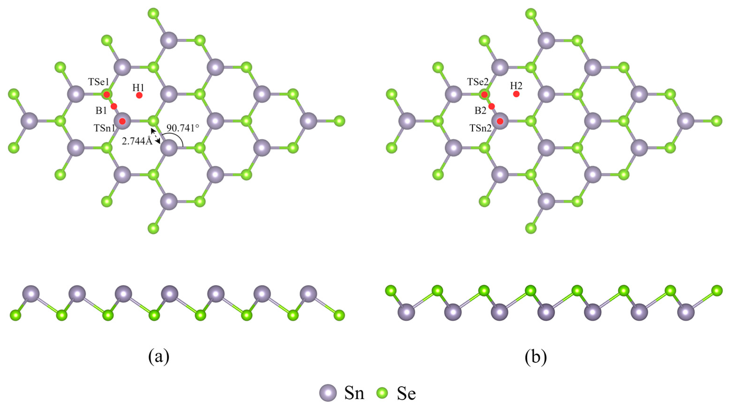
Figure 1. The structure and adsorption position of the SnSe monolayer: (a) Sn side; (b) Se side.
Micromachines 15 00960 g001
Figure 2. The most stable configuration (a) and differential charge density (b) of O3-adsopred SnSe monolayer.
Micromachines 15 00960 g002
Figure 3. Band structures of pristine (a) and O3-adsorbed (b) SnSe monolayers.
Micromachines 15 00960 g003
Figure 4. Total and partial DOSs of SnSe monolayer: (a) TDOSs and PDOSs of (b) O, (c) Sn, (d) Se (Fermi level is set as 0 eV).
Micromachines 15 00960 g004
Figure 5. The recovery time (τ) for O3 adsorbed on SnSe monolayers at different temperatures (T).
Micromachines 15 00960 g005
Figure 6. The current-voltage characteristics of pristine and O3-adsorped SnSe monolayers.
Micromachines 15 00960 g006
Figure 7. The sensitivity of O3-adsorped SnSe monolayers at temperatures of 298 K and 698 K.
Micromachines 15 00960 g007
Disclaimer/Publisher’s Note: The statements, opinions and data contained in all publications are solely those of the individual author(s) and contributor(s) and not of MDPI and/or the editor(s). MDPI and/or the editor(s) disclaim responsibility for any injury to people or property resulting from any ideas, methods, instructions or products referred to in the content.