
A Low-Power Optoelectronic Receiver IC for Short-Range LiDAR Sensors in 180 nm CMOS


Abstract
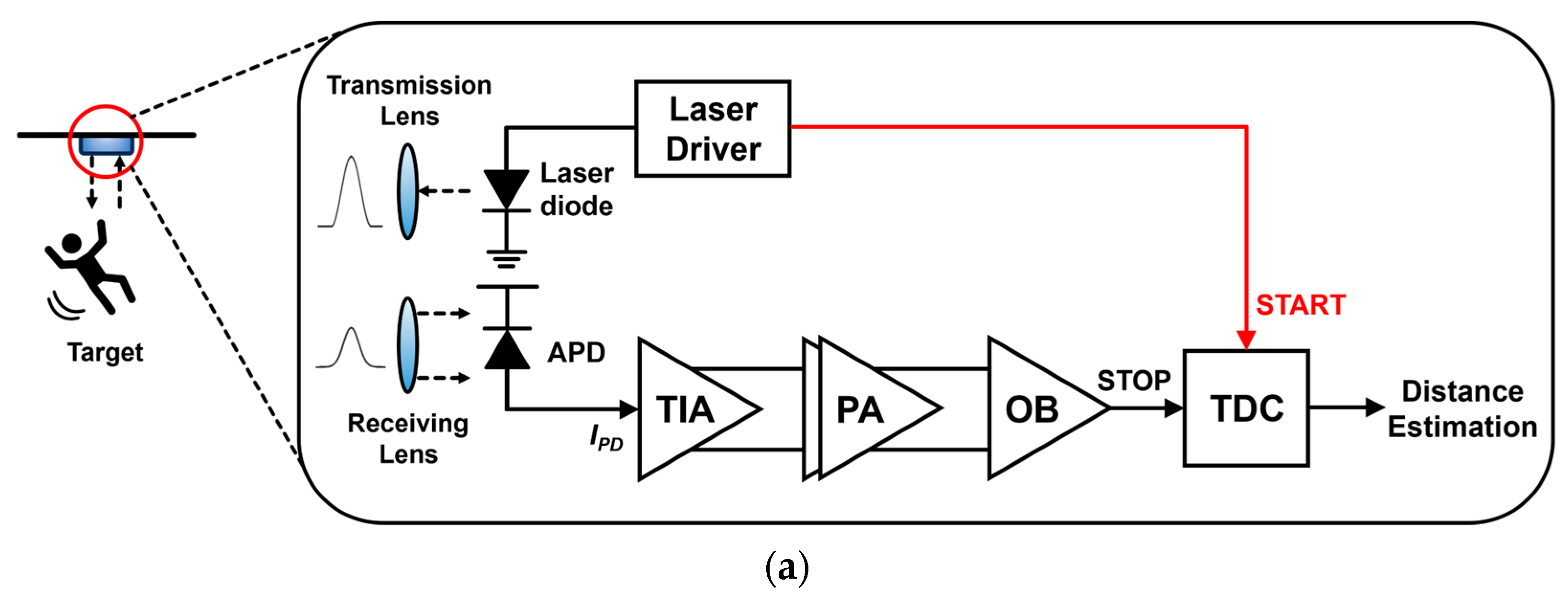
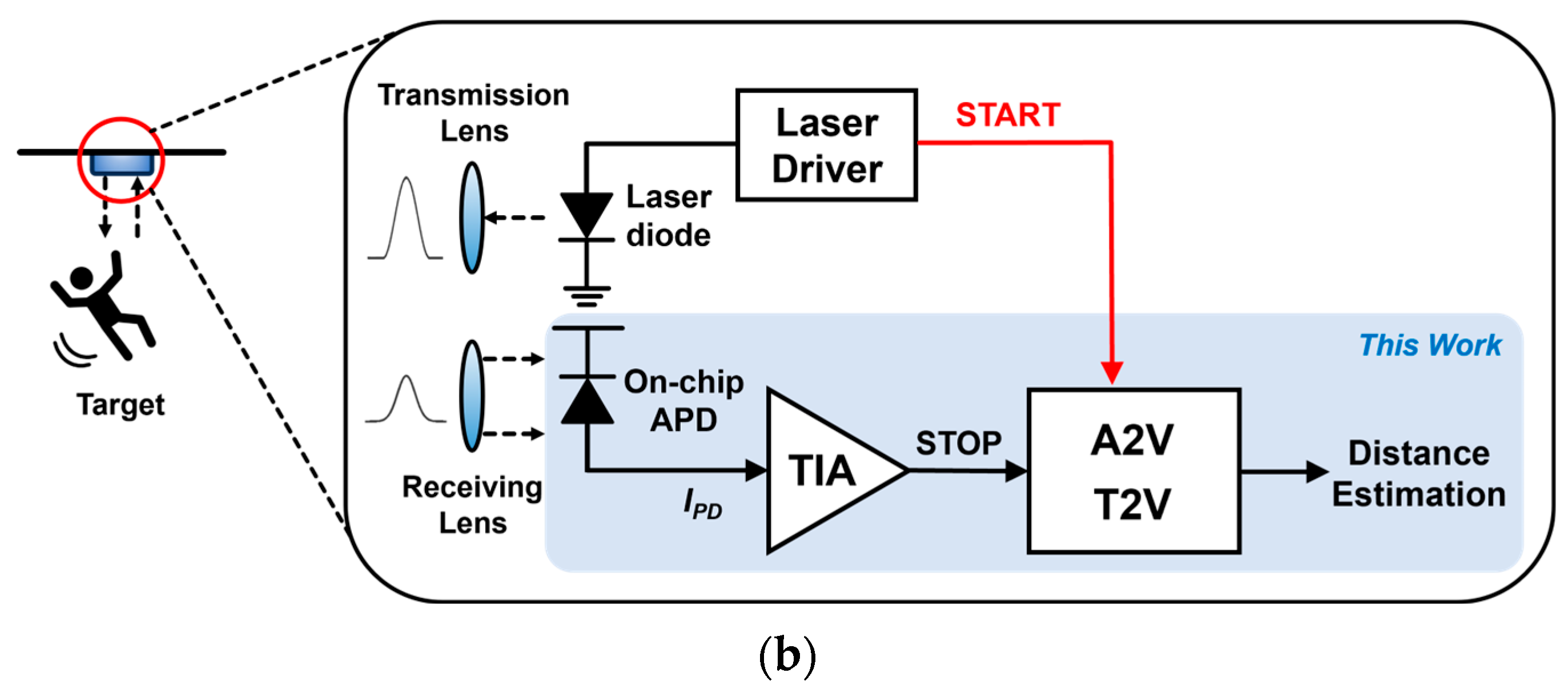
1. Introduction
2. Circuit Description
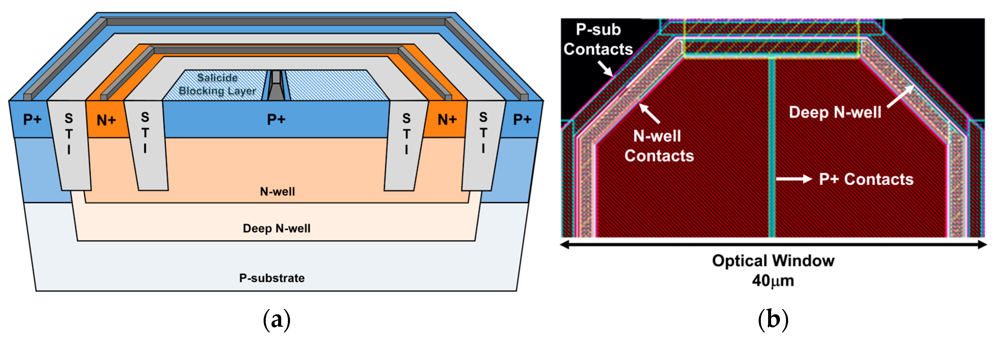
2.1. On-Chip P+/NW/DNW APD
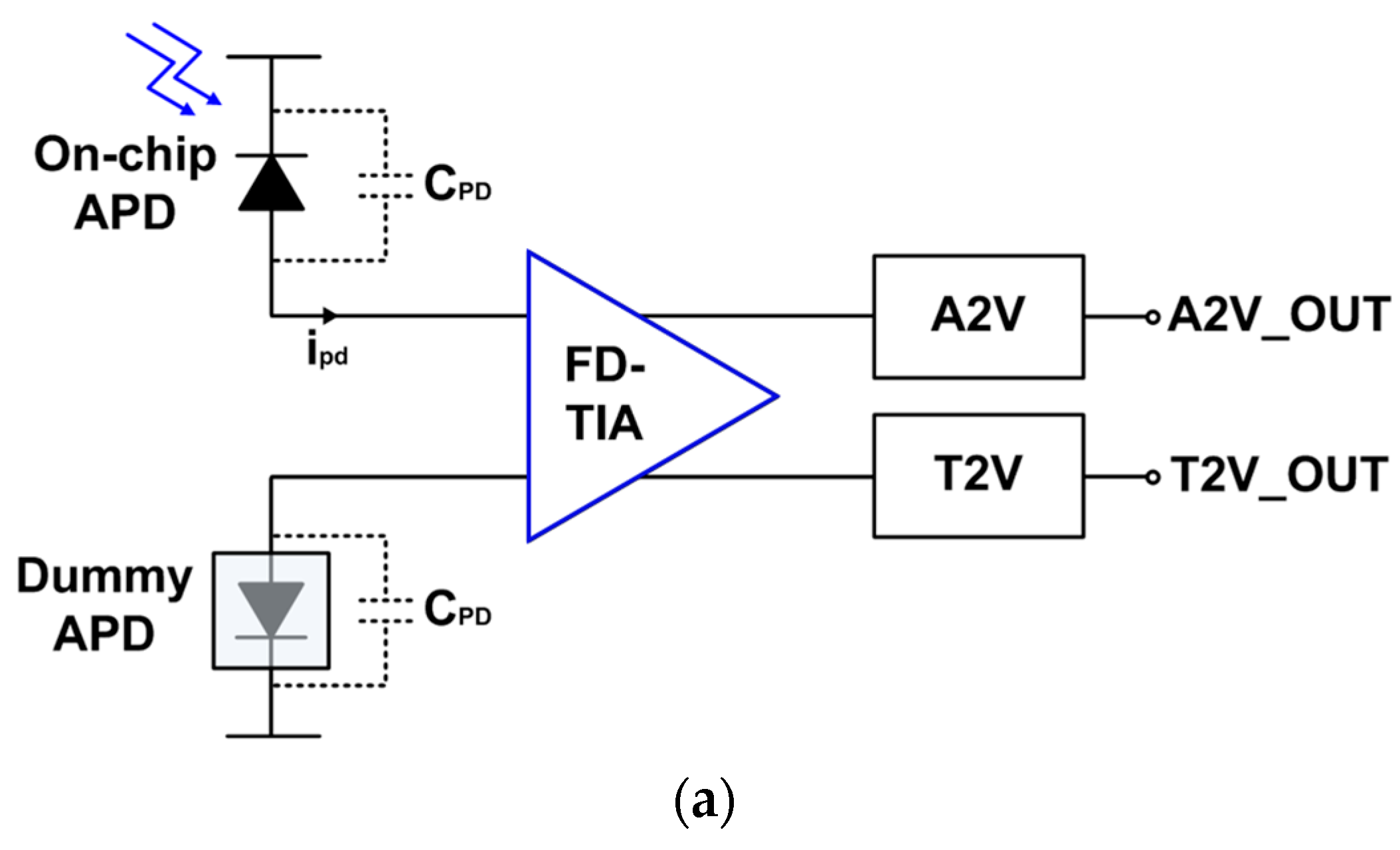
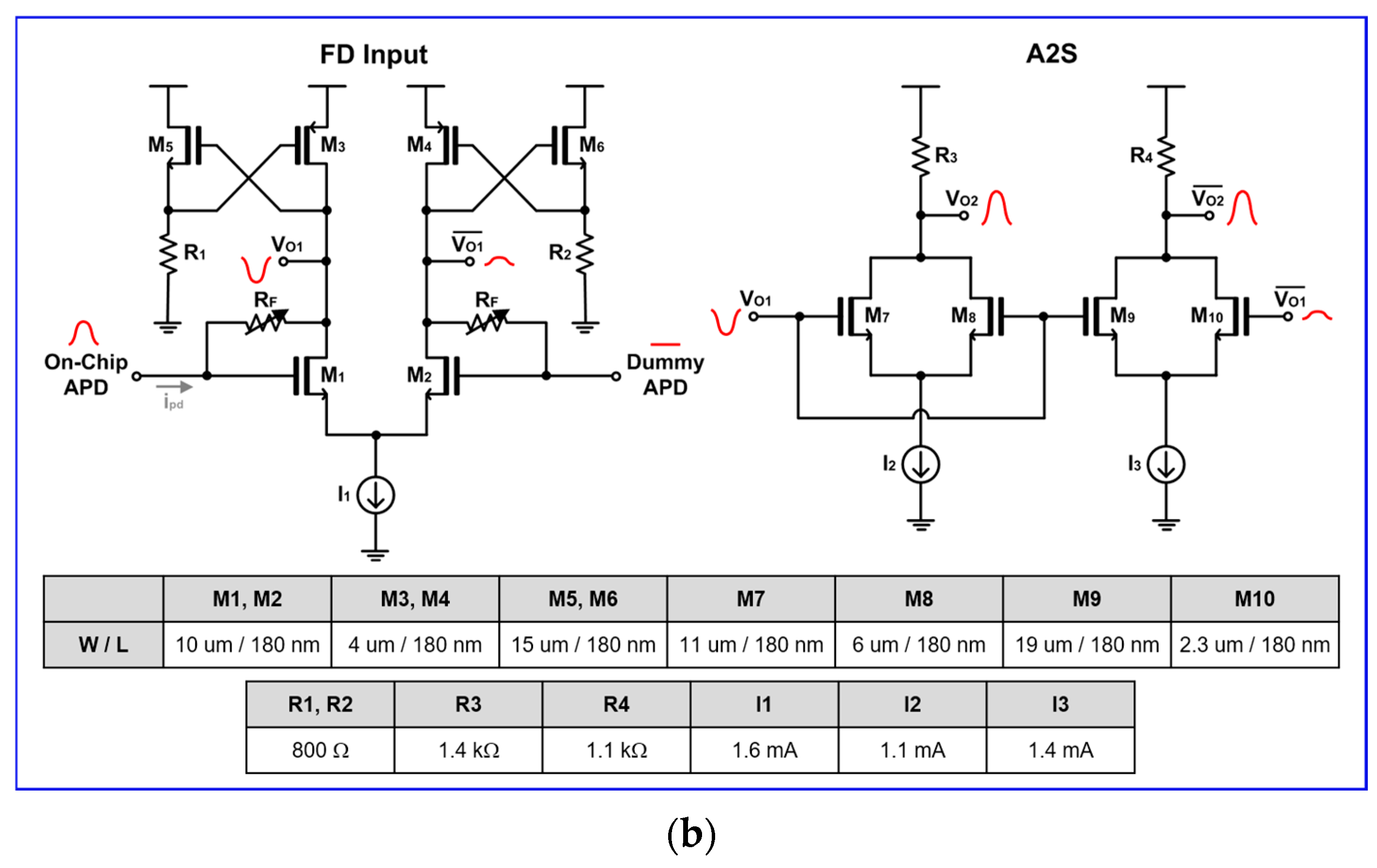
2.2. Fully Differential Transimpedance Amplifier (FD-TIA)
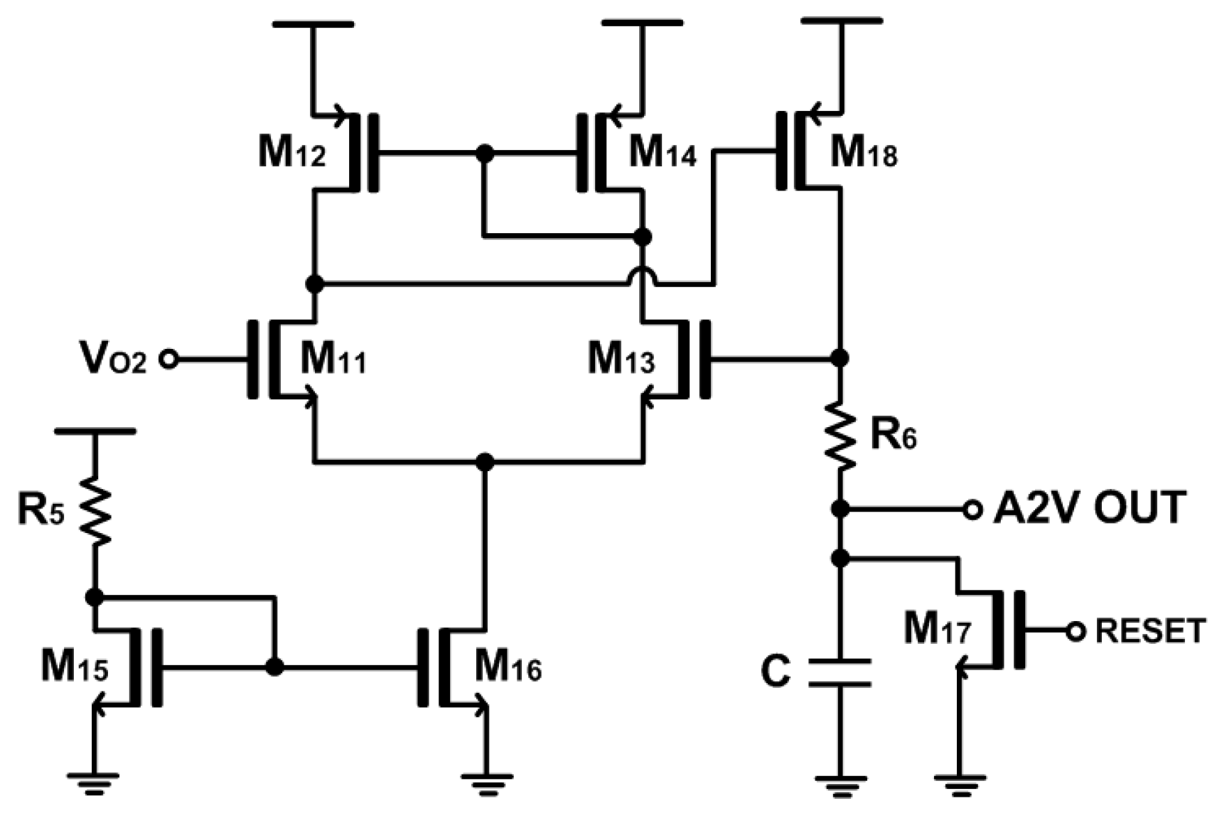
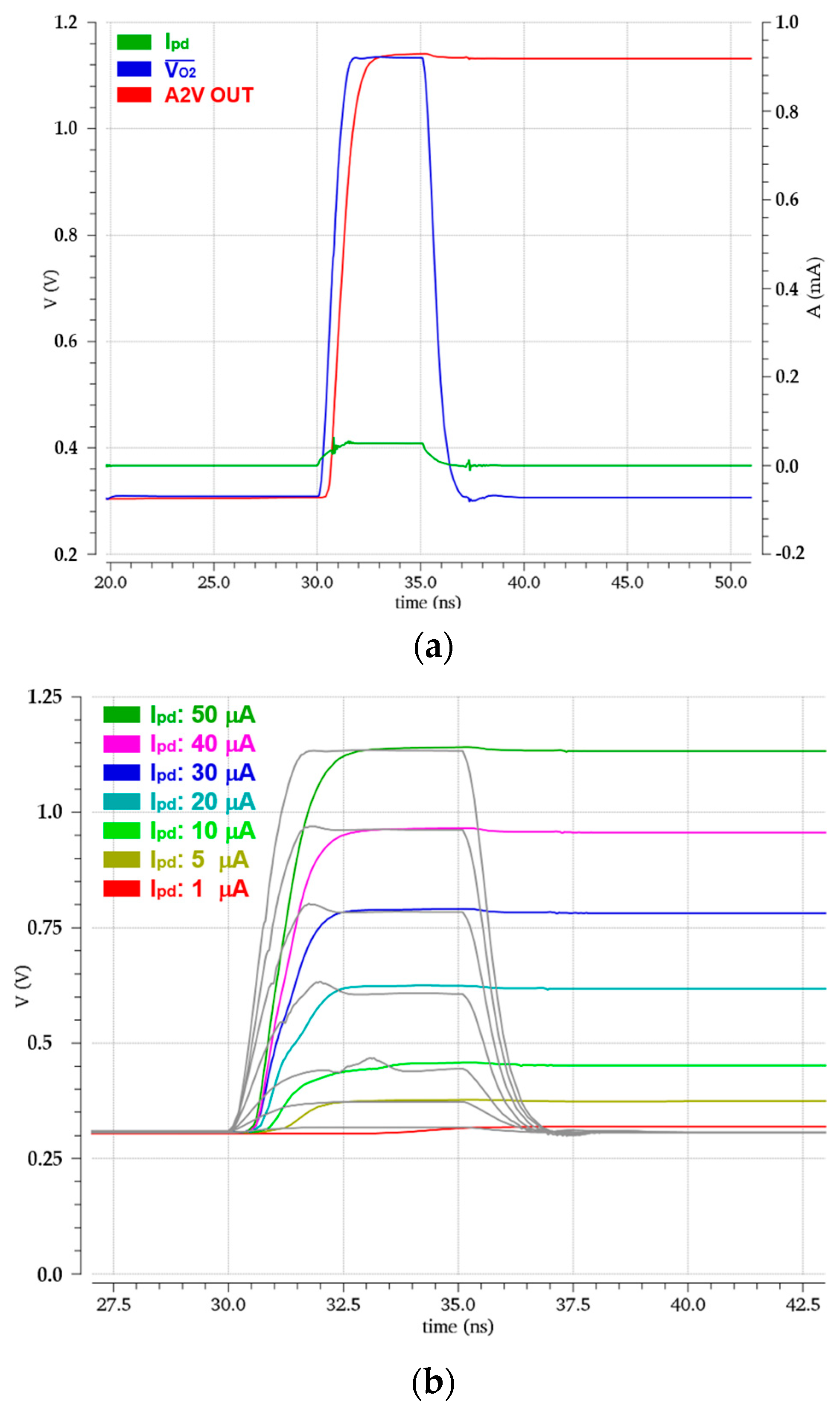
2.3. A2V Converter
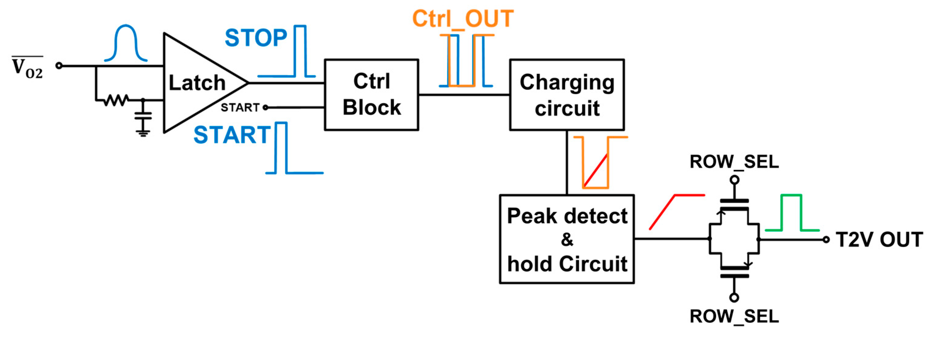
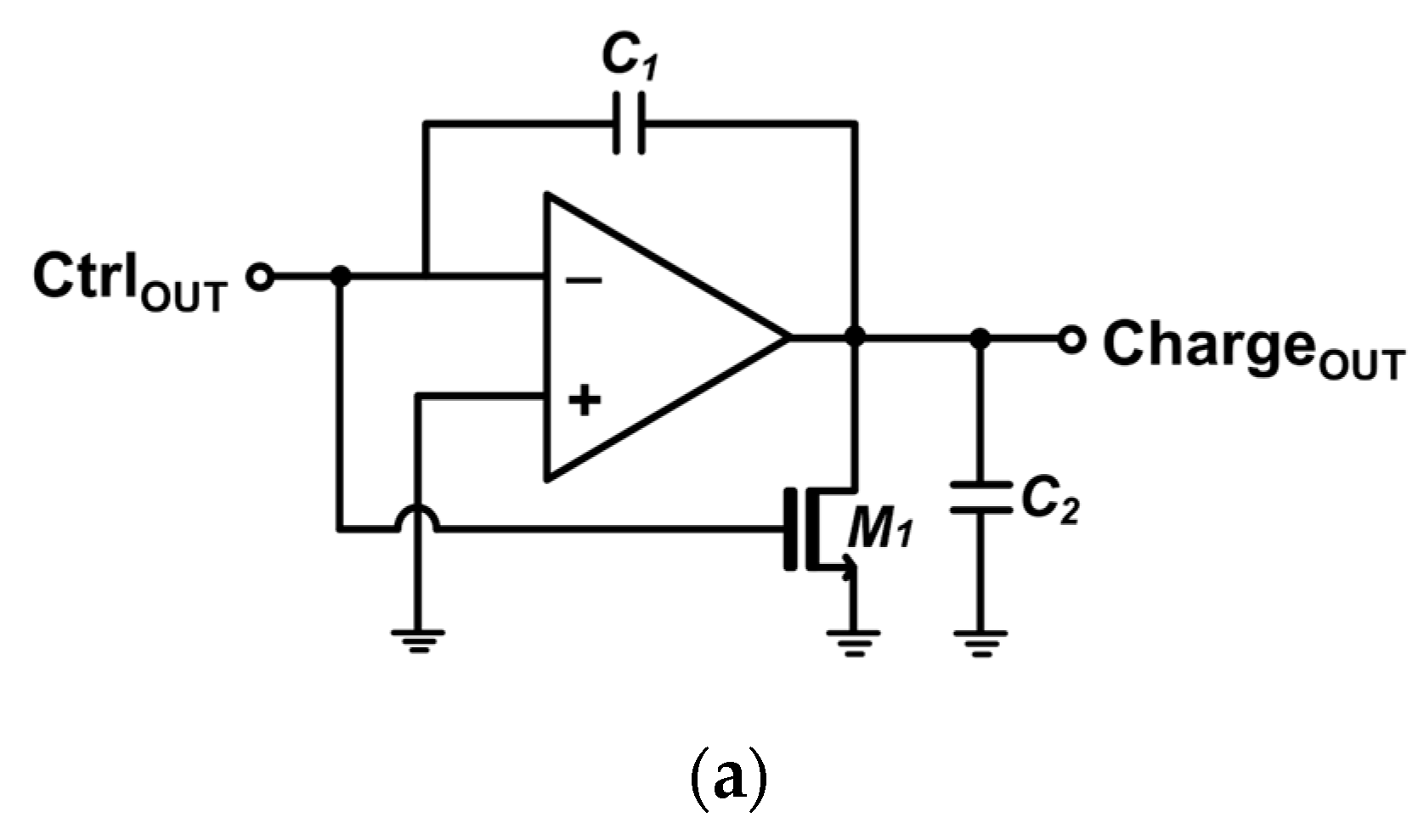
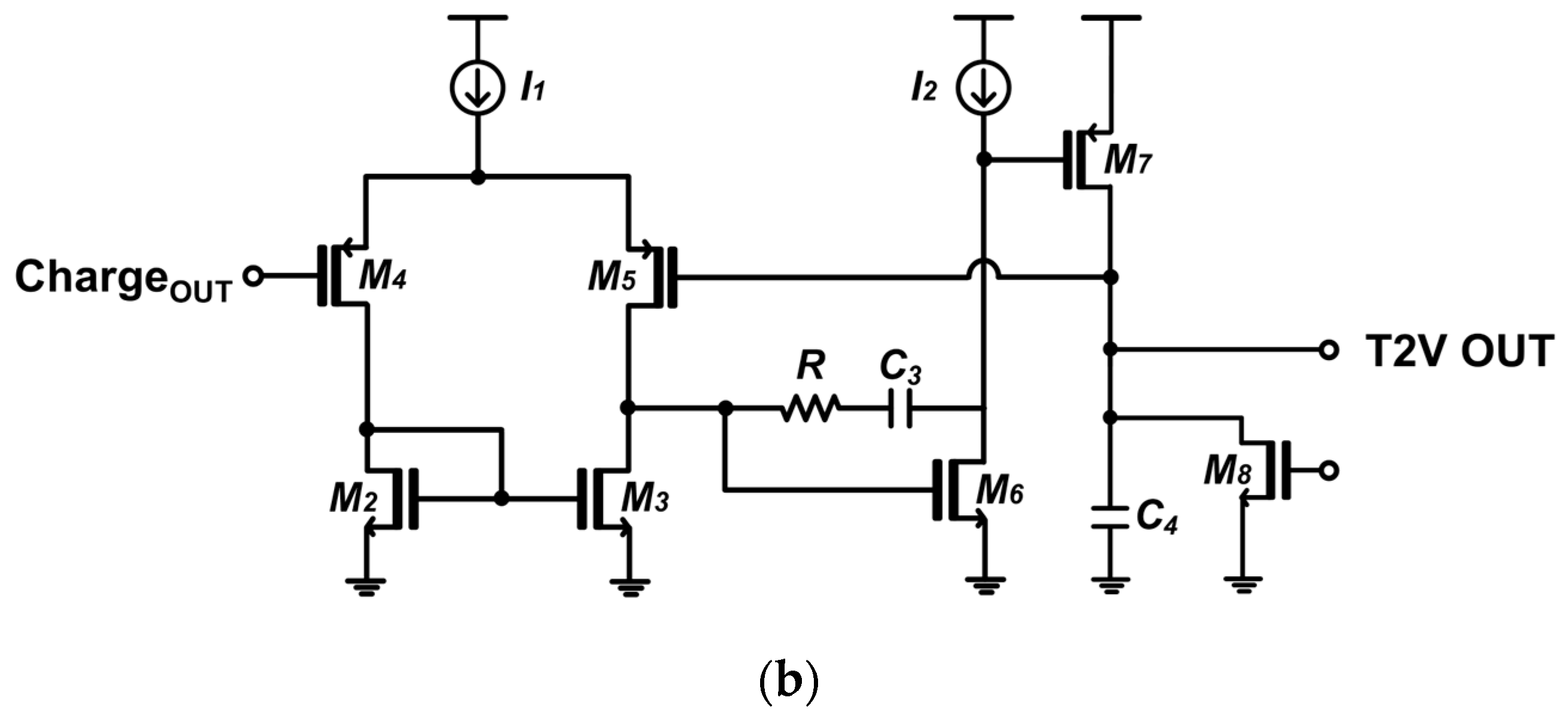
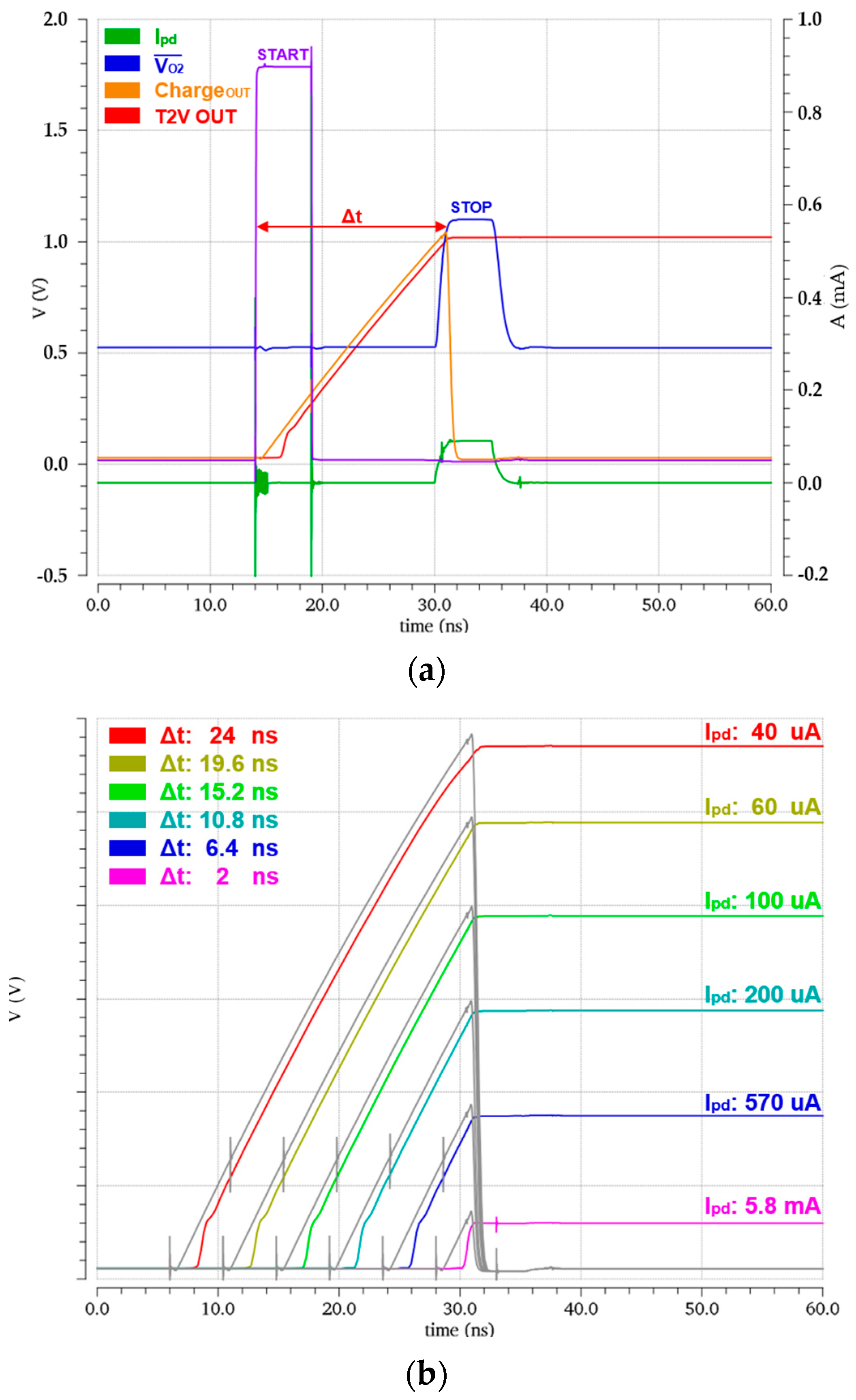
2.4. T2V Converter
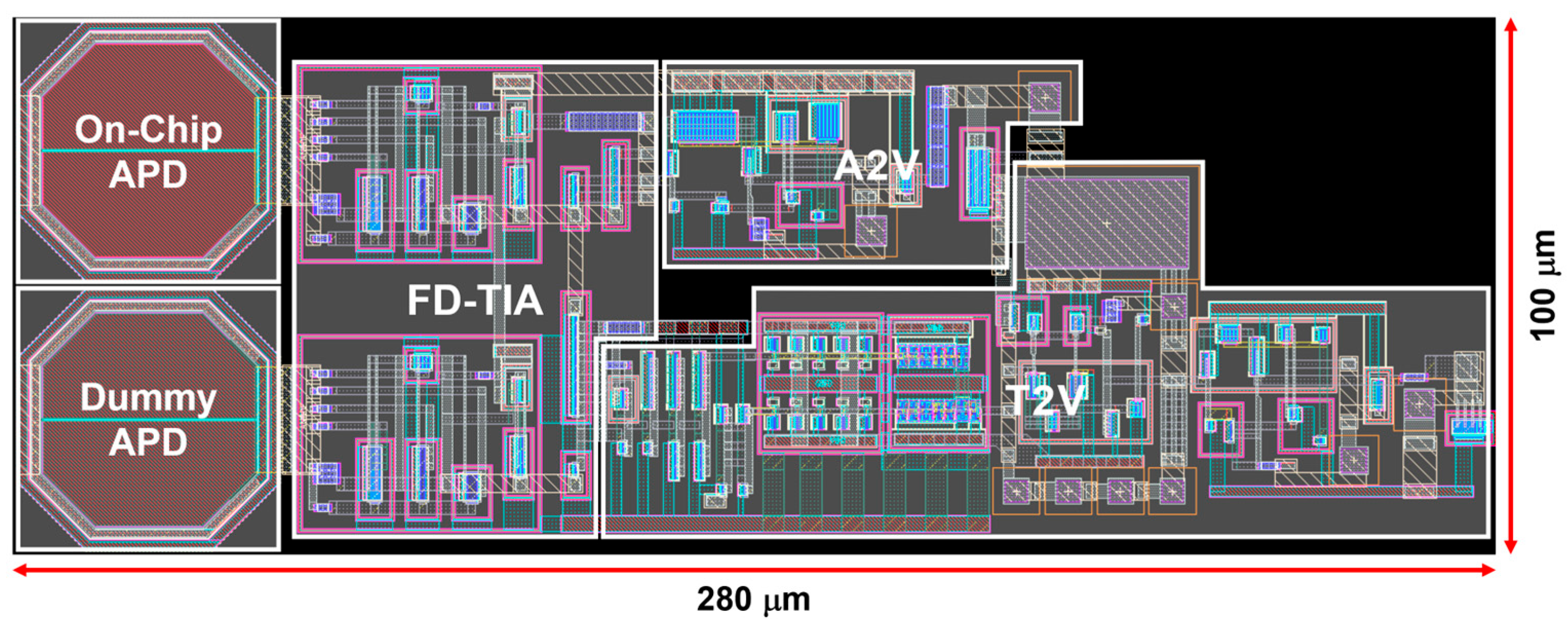
3. Chip Layout and Post-Layout Simulation Results

| Parameters | [15] | [16] | [17] | [18] | This Work | |
|---|---|---|---|---|---|---|
| CMOS technology (nm) | 350 | 180 | 180 | 350 | 180 | |
| APD | Type | Off-chip | ‡ Off-chip | ‡ Off-chip | Off-chip | On-chip |
| Cpd (pF) | 3 | 2 | 3 | 4 | 0.5 | |
| Responsivity (A/W) | 40 | - | - | - | 4.16 | |
| Wavelength (nm) | 905 | - | - | 905 | 850 | |
| Max. TZ gain (dBΩ) | 100 | 83.5 | 100 | 121 | 81.2 | |
| Gain control | No | Yes | Yes | No | Yes | |
| Bandwidth (MHz) | 230 | 89 | 180 | 230 | 842 | |
| Min. detectable current (µApp) | 1.0 | 1.3 | 5 | 0.6 | 1.0 | |
| Max. detectable current (mApp) | 39 ξ | 2.06 | 2 | 30 | 5.8 | |
| Dynamic range (dB) | 92 | 64 | 52 | 94 | 75.3 | |
| Power dissipation per channel (mW) (DC bias current consumption) | 330 * (100 mA) | 45 * (13.6 mA) | 49.3/10.5 (27.4/5.83 mA) | 155 * (47 mA) | 10 (5.56 mA) | |
| FoM ψ | 70 | 165 | 365 | 180 | 6837 | |
| Chip area (mm2) | 4 (Rx 1ch) 10 (TDC) | 2.52 (8ch †) | 5 (Rx 8ch) | 2.89 (Rx 1ch) | 1 (Rx 3ch) | |
4. Conclusions
Author Contributions
Funding
Data Availability Statement
Acknowledgments
Conflicts of Interest
References
- Raj, T.; Hanim Hashim, F.; Baseri Huddin, A.; Ibrahim, M.F.; Hussain, A. A Survey on LiDAR Scanning Mechanisms. Electronics 2020, 9, 741. [Google Scholar] [CrossRef]
- Yoon, D.; Joo, J.-E.; Park, S.M. Mirrored Current-Conveyor Transimpedance Amplifier for Home Monitoring LiDAR Sensors. IEEE Sens. J. 2021, 21, 5589–5597. [Google Scholar] [CrossRef]
- Frøvik, N.; Malekzai, B.A.; Øvsthus, K. Utilising LiDAR for fall detection. Health Technol. Lett. 2021, 8, 11–17. [Google Scholar] [CrossRef] [PubMed]
- Fraccaro, P.; Evangelopoulos, X.; Edwards, B. Development and Preliminary Evaluation of a Method for Passive, Privacy-Aware Home Care Monitoring Based on 2D LiDAR Data. In Artificial Intelligence in Medicine: 18th International Conference on Artificial Intelligence in Medicine, AIME 2020, Minneapolis, MN, USA, 25–28 August 2020; Springer International Publishing: Berlin/Heidelberg, Germany, 2020. [Google Scholar]
- Wang, Y.-T.; Peng, C.-C.; Ravankar, A.A.; Ravankar, A. A Single LiDAR-Based Feature Fusion Indoor Localization Algorithm. Sensors 2018, 18, 1294. [Google Scholar] [CrossRef] [PubMed]
- Yan, Z.; Wang, H.; Wang, Z.; Liu, X.; Ning, Q. Imaging simulation of the AMCW ToF camera based on path tracking. Appl. Opt. 2022, 61, 5474–5482. [Google Scholar] [CrossRef] [PubMed]
- Rogers, C.; Piggott, A.Y.; Thomson, D.J.; Wiser, R.F.; Opris, I.E.; Fortune, S.A.; Compston, A.J.; Gondarenko, A.; Meng, F.; Chen, X.; et al. A Universal 3D Imaging Sensor on a Silicon Photonics Platform. Nature 2021, 590, 256–261. [Google Scholar] [CrossRef] [PubMed]
- Zhang, X.; Kwon, K.; Henriksson, J.; Luo, J.; Wu, M.C. A Large-Scale Microelectromechanical-Systems-Based Silicon Photonics LiDAR. Nature 2022, 603, 253–258. [Google Scholar] [CrossRef] [PubMed]
- Park, J.; Jeong, B.G.; Kim, S.I.; Lee, D.; Kim, J.; Shin, C.; Lee, C.B.; Otsuka, T.; Kyoung, J.; Kim, S. All-Solid-State Spatial Light Modulator with Independent Phase and Amplitude Control for Three-Dimensional LiDAR Applications. Nat. Nanotechnol. 2021, 16, 69–76. [Google Scholar] [CrossRef] [PubMed]
- Zang, X.; Yao, B.; Chen, L.; Xie, J.; Guo, X.; Balakin, A.V.; Shkurinov, A.P.; Zhuang, S. Metasurfaces for Manipulating Terahertz Waves. Light Adv. Manuf. 2021, 2, 10. [Google Scholar]
- Nguyen, V.N.; Duong, D.N.; Chung, Y.; Lee, J.W. A Cyclic Vernier Two-Step TDC for High Input Range Time-of-Flight Sensor Using Startup Time Correction Technique. Sensors 2018, 18, 3948. [Google Scholar] [CrossRef] [PubMed]
- He, Y.; Park, S.M. A CMOS Integrator-Based Clock-Free Time-to-Digital Converter for Home-Monitoring LiDAR Sensors. Sensors 2022, 22, 554. [Google Scholar] [CrossRef] [PubMed]
- Liu, M.; Liu, H.; Li, X.; Zhu, Z. A 60-m range 6.16-mW laser-power linear-mode LiDAR system with multiplex ADC/TDC in 65-nm CMOS. IEEE Trans. Circuits Syst. I Reg. Pap. 2019, 67, 753–764. [Google Scholar] [CrossRef]
- Lee, M.-J.; Choi, W.-Y. Effects of parasitic resistance on the performance of silicon avalanche photodetectors in standard CMOS technology. IEEE Electron Device Lett. 2015, 37, 60–63. [Google Scholar] [CrossRef]
- Kurtti, S.; Jansson, J.-P.; Kostamovaara, J. A CMOS Receiver–TDC Chip Set for Accurate Pulsed TOF Laser Ranging. IEEE Trans. Instrum. Meas. 2020, 69, 2208–2217. [Google Scholar] [CrossRef]
- Ye, M.; Zheng, X.; Li, Y.; Zhao, Y. A Low-Complexity Hybrid Readout Circuit for Lidar Receiver. IEEE Trans. Very Large Scale Integr. (VLSI) Syst. 2020, 28, 828–832. [Google Scholar] [CrossRef]
- Yang, Y.; Liu, X.; Yang, R.; Ma, S.; Xia, Y.; Li, J.; Zhang, B.; Geng, L.; Li, D. A Low-Power Multimode Eight-Channel AFE for dToF LiDAR. In Proceedings of the 2024 IEEE International Symposium on Circuits and Systems (ISCAS), Singapore, 19–22 May 2024. [Google Scholar]
- Baharmast, A.; Kurtti, S.; Kostamovaara, J. A wide dynamic range laser radar receiver based on input pulse-shaping techniques. IEEE Trans. Circuits Syst. I Reg. Pap. 2020, 67, 2566–2577. [Google Scholar] [CrossRef]
| Parameters | SS 1.62 V, −45 °C | TT 1.8 V, 27 °C | FF 1.98 V, 125 °C | |
|---|---|---|---|---|
| FD-TIA | TZ gain (dBΩ) | 84.5 (+4.1%) | 81.2 | 77.9 (−4.1%) |
| Bandwidth (GHz) | 839 (−0.36%) | 842 | 854 (+1.43%) | |
| ) | 8.67 (−14%) | 10.1 | 12.3 (+22%) | |
| A2V | Output voltage amplitude (mVpp) @ 1 µApp input current | 327 (+2.2%) | 320 | 343 (+7.2%) |
| Output voltage amplitude (Vpp) @ 50 µApp input current | 0.96 (−14%) | 1.12 | 1.27 (+13%) | |
| T2V | Output voltage amplitude (Vpp) @ 40 µApp (Δt = 24 ns) input current | 1.16 (−19%) | 1.43 | 1.72 (+20%) |
| Output voltage amplitude (mVpp) @ 5.8 mApp (Δt = 2 ns) input current | 106 (−27%) | 146 | 187 (+28%) | |
Disclaimer/Publisher’s Note: The statements, opinions and data contained in all publications are solely those of the individual author(s) and contributor(s) and not of MDPI and/or the editor(s). MDPI and/or the editor(s) disclaim responsibility for any injury to people or property resulting from any ideas, methods, instructions or products referred to in the content. |
© 2024 by the authors. Licensee MDPI, Basel, Switzerland. This article is an open access article distributed under the terms and conditions of the Creative Commons Attribution (CC BY) license (https://creativecommons.org/licenses/by/4.0/).
Share and Cite
Choi, S.; Chon, Y.; Park, S.M. A Low-Power Optoelectronic Receiver IC for Short-Range LiDAR Sensors in 180 nm CMOS. Micromachines 2024, 15, 1066. https://doi.org/10.3390/mi15091066
Choi S, Chon Y, Park SM. A Low-Power Optoelectronic Receiver IC for Short-Range LiDAR Sensors in 180 nm CMOS. Micromachines. 2024; 15(9):1066. https://doi.org/10.3390/mi15091066
Chicago/Turabian StyleChoi, Shinhae, Yeojin Chon, and Sung Min Park. 2024. "A Low-Power Optoelectronic Receiver IC for Short-Range LiDAR Sensors in 180 nm CMOS" Micromachines 15, no. 9: 1066. https://doi.org/10.3390/mi15091066
APA StyleChoi, S., Chon, Y., & Park, S. M. (2024). A Low-Power Optoelectronic Receiver IC for Short-Range LiDAR Sensors in 180 nm CMOS. Micromachines, 15(9), 1066. https://doi.org/10.3390/mi15091066