
Ultra-Broadband Mode (De)Multiplexer on Thin-Film Lithium Niobate Platform Adopting Phase Control Theory


Abstract
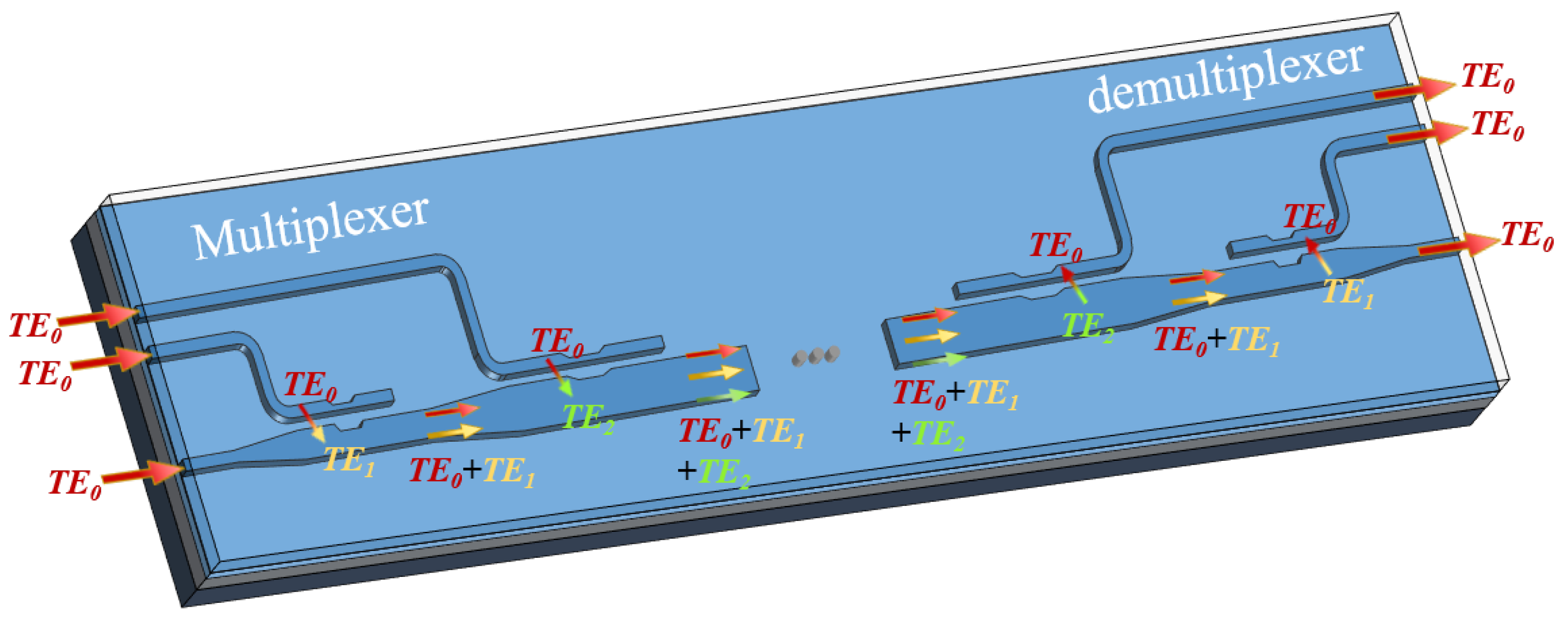
1. Introduction
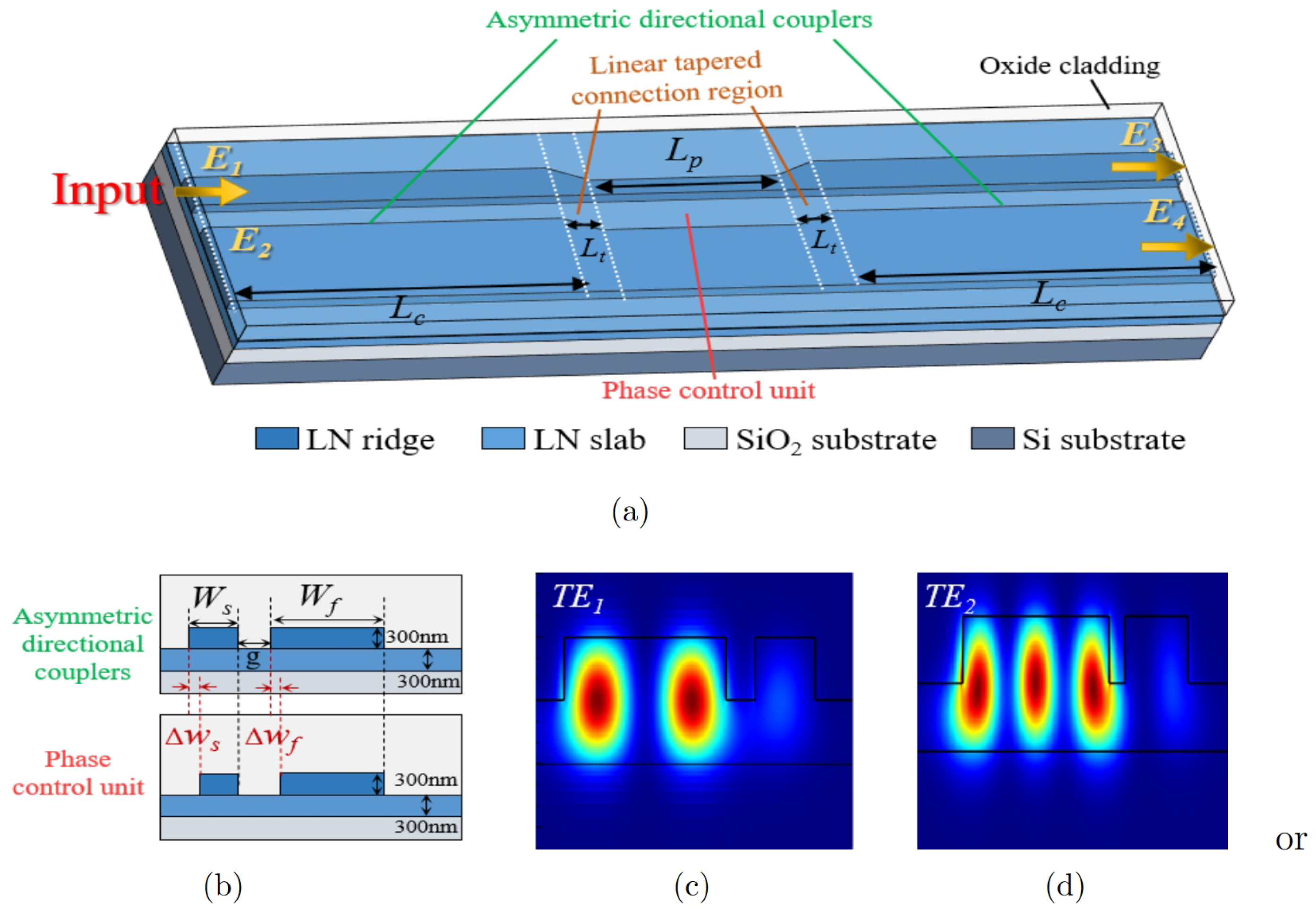
2. Device Design and Method
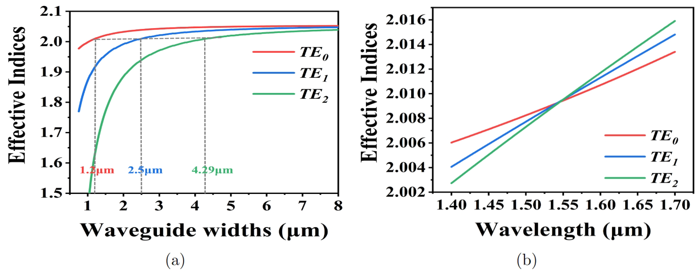
2.1. Structure and Theoretical Analysis
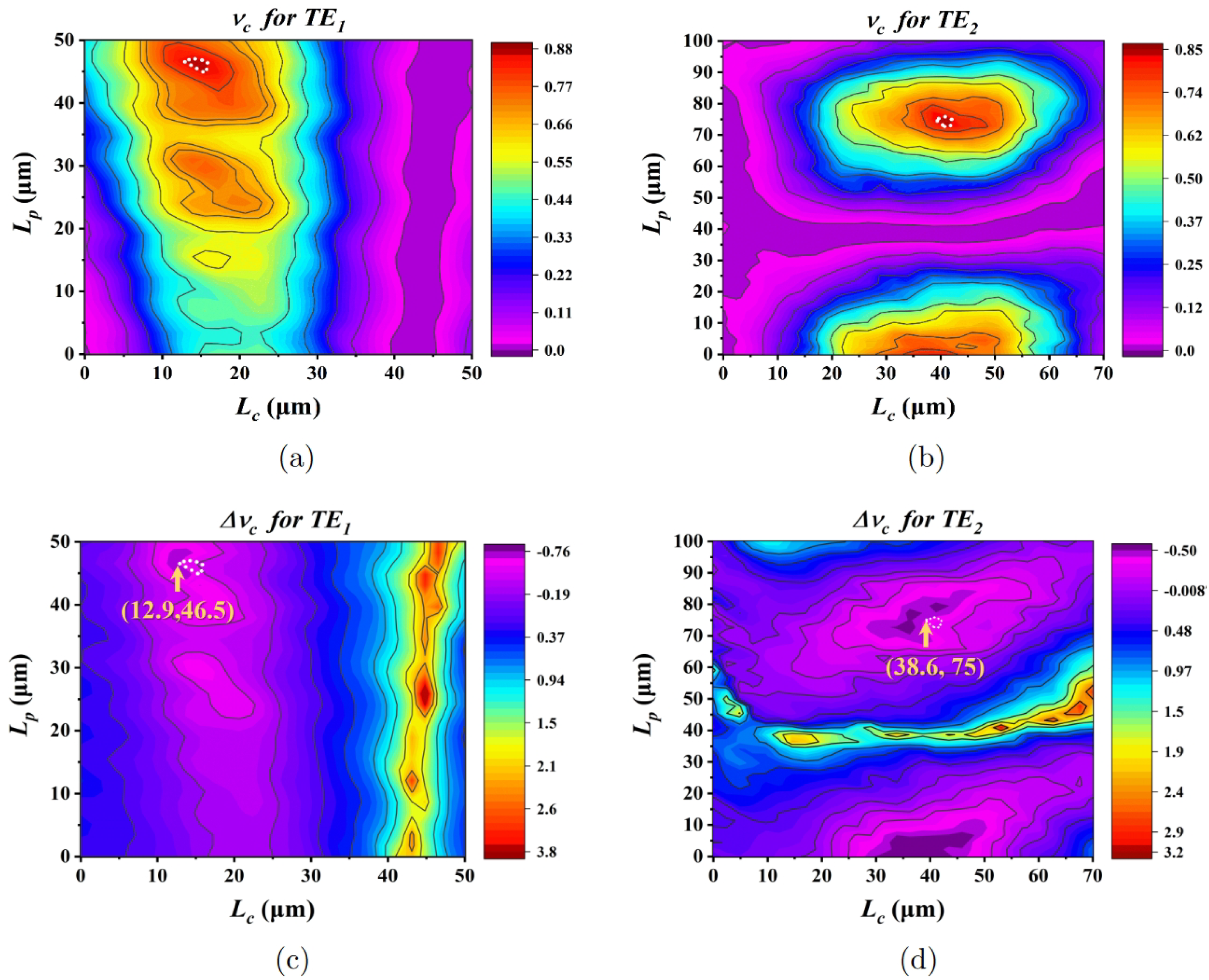
2.2. Three-Dimensional FDTD Simulation
3. Conclusions
Author Contributions
Funding
Data Availability Statement
Acknowledgments
Conflicts of Interest
References
- Khonina, S.N.; Kazanskiy, N.L.; Butt, M.A.; Karpeev, S.V. Optical multiplexing techniques and their marriage for on-chip and optical fiber communication: A review. Opto-Electron. Adv. 2022, 5, 210127. [Google Scholar] [CrossRef]
- Wang, J.; Long, Y. On-chip silicon photonic signaling and processing: A review. Sci. Bull. 2018, 63, 1267–1310. [Google Scholar] [CrossRef] [PubMed]
- Chen, Z.; Zhu, Y.; Ruan, X.; Li, Y.; Li, Y.; Zhang, F. Bridged Coupler and Oval Mode Converter Based Silicon Mode Division (De)Multiplexer and Terabit WDM-MDM System Demonstration. J. Light. Technol. 2018, 36, 2757–2766. [Google Scholar] [CrossRef]
- Ding, Y.; Xu, J.; Ros, F.D.; Huang, B.; Ou, H.; Peucheret, C. On-chip two-mode division multiplexing using tapered directional coupler-based mode multiplexer and demultiplexer. Opt. Express 2013, 21, 10376–10382. [Google Scholar] [CrossRef]
- Zhang, Z.; Hu, X.; Wang, J. On-chip optical mode exchange using tapered directional coupler. Sci. Rep. 2015, 5, 16072. [Google Scholar] [CrossRef] [PubMed]
- Huang, Q.; Wu, Y.; Jin, W.; Chiang, K.S. Mode Multiplexer With Cascaded Vertical Asymmetric Waveguide Directional Couplers. J. Light. Technol. 2018, 36, 2903–2911. [Google Scholar] [CrossRef]
- Sun, Q.; Chen, H.; Wang, J.; Yang, J.; Jia, H. Broadband mode-division (de) multiplexer using nanorod-assisted multimode subwavelength gratings. Opt. Commun. 2024, 552, 130037. [Google Scholar] [CrossRef]
- González-Andrade, D.; Dias, A.; Wangüemert-Pérez, J.G.; Ortega-Moñux, A.; Molina-Fernández, I.; Halir, R.; Cheben, P.; Velasco, A.V. Experimental demonstration of a broadband mode converter and multiplexer based on subwavelength grating waveguides. Opt. Laser Technol. 2020, 129, 106297. [Google Scholar] [CrossRef]
- Uematsu, T.; Ishizaka, Y.; Kawaguchi, Y.; Saitoh, K.; Koshiba, M. Design of a Compact Two-Mode Multi/Demultiplexer Consisting of Multimode Interference Waveguides and a Wavelength-Insensitive Phase Shifter for Mode-Division Multiplexing Transmission. J. Light. Technol. 2012, 30, 2421–2426. [Google Scholar] [CrossRef]
- González-Andrade, D.; Olivares, I.; de Cabo, R.F.; Vilas, J.; Dias, A.; Velasco, A.V. Broadband three-mode converter and multiplexer based on cascaded symmetric Y-junctions and subwavelength engineered MMI and phase shifters. Opt. Laser Technol. 2023, 164, 109513. [Google Scholar] [CrossRef]
- Chang, W.; Lu, L.; Ren, X.; Li, D.; Pan, Z.; Cheng, M.; Liu, D.; Zhang, M. Ultra-compact mode (de) multiplexer based on subwavelength asymmetric Y-junction. Opt. Express 2018, 26, 8162–8170. [Google Scholar] [CrossRef]
- Chen, W.; Wang, P.; Yang, T.; Wang, G.; Dai, T.; Zhang, Y.; Zhou, L.; Jiang, X.; Yang, J. Silicon three-mode (de)multiplexer based on cascaded asymmetric Y junctions. Opt. Lett. 2016, 41, 2851–2854. [Google Scholar] [CrossRef] [PubMed]
- He, Y.; Li, X.; Zhang, Y.; An, S.; Wang, H.; Wang, Z.; Chen, H.; Huang, Y.; Huang, H.; Fontaine, N.K.; et al. On-chip metamaterial-enabled high-order mode-division multiplexing. Adv. Photonics 2023, 5, 056008. [Google Scholar] [CrossRef]
- Li, C.; Liu, D.; Dai, D. Multimode silicon photonics. Nanophotonics 2019, 8, 227–247. [Google Scholar] [CrossRef]
- Han, X.; Jiang, Y.; Frigg, A.; Xiao, H.; Zhang, P.; Nguyen, T.G.; Boes, A.; Yang, J.; Ren, G.; Su, Y.; et al. Mode and polarization-division multiplexing based on silicon nitride loaded lithium niobate on insulator platform. Laser Photonics Rev. 2022, 16, 2100529. [Google Scholar] [CrossRef]
- Chen, G.; Li, N.; Ng, J.D.; Lin, H.L.; Zhou, Y.; Fu, Y.H.; Lee, L.Y.T.; Yu, Y.; Liu, A.Q.; Danner, A.J. Advances in lithium niobate photonics: Development status and perspectives. Adv. Photonics 2022, 4, 034003. [Google Scholar] [CrossRef]
- Zhang, M.; Ai, W.; Chen, K.; Jin, W.; Chiang, K.S. A Lithium-Niobate Waveguide Directional Coupler for Switchable Mode Multiplexing. IEEE Photonics Technol. Lett. 2018, 30, 1764–1767. [Google Scholar] [CrossRef]
- Lukas, C.; Hochberg, M. Silicon Photonics Design: From Devices to Systems; Cambridge University Press: Cambridge, UK, 2015. [Google Scholar]
- Mackay, T.G.; Lakhtakia, A. The Transfer-Matrix Method in Electromagnetics and Optics; Springer Nature: Berlin/Heidelberg, Germany, 2020. [Google Scholar]
- Available online: https://www.lumerical.com/ (accessed on 1 August 2024).
- Yu, Z.; Tong, Y.; Tsang, H.K.; Sun, X. High-dimensional communication on etchless lithium niobate platform with photonic bound states in the continuum. Nat. Commun. 2020, 11, 2602. [Google Scholar] [CrossRef] [PubMed]
- Zhu, W.; Deng, C.; Wang, D.; Wang, Q.; Sun, Y.; Wang, J.; Yun, B.; Cui, Y.; Hu, G. Four-Channel Broadband Mode (De) multiplexer Based on Thin-Film Lithium Niobate Platform. ACS Photonics 2024, 11, 2700–2706. [Google Scholar] [CrossRef]


Disclaimer/Publisher’s Note: The statements, opinions and data contained in all publications are solely those of the individual author(s) and contributor(s) and not of MDPI and/or the editor(s). MDPI and/or the editor(s) disclaim responsibility for any injury to people or property resulting from any ideas, methods, instructions or products referred to in the content. |
© 2024 by the authors. Licensee MDPI, Basel, Switzerland. This article is an open access article distributed under the terms and conditions of the Creative Commons Attribution (CC BY) license (https://creativecommons.org/licenses/by/4.0/).
Share and Cite
Yin, K.; Jiao, W.; Wang, L.; Zhu, S. Ultra-Broadband Mode (De)Multiplexer on Thin-Film Lithium Niobate Platform Adopting Phase Control Theory. Micromachines 2024, 15, 1084. https://doi.org/10.3390/mi15091084
Yin K, Jiao W, Wang L, Zhu S. Ultra-Broadband Mode (De)Multiplexer on Thin-Film Lithium Niobate Platform Adopting Phase Control Theory. Micromachines. 2024; 15(9):1084. https://doi.org/10.3390/mi15091084
Chicago/Turabian StyleYin, Kun, Wenting Jiao, Lin Wang, and Shiqiang Zhu. 2024. "Ultra-Broadband Mode (De)Multiplexer on Thin-Film Lithium Niobate Platform Adopting Phase Control Theory" Micromachines 15, no. 9: 1084. https://doi.org/10.3390/mi15091084
APA StyleYin, K., Jiao, W., Wang, L., & Zhu, S. (2024). Ultra-Broadband Mode (De)Multiplexer on Thin-Film Lithium Niobate Platform Adopting Phase Control Theory. Micromachines, 15(9), 1084. https://doi.org/10.3390/mi15091084