
Key Technologies in Developing Chip-Scale Hot Atomic Devices for Precision Quantum Metrology

 ,
,
Abstract
:1. Introduction
2. Vapor Cells
2.1. Glass-Blowing Technique
2.2. MEMS Vapor Cell Fabrication
2.2.1. Introduction of Alkali Atoms and Gases
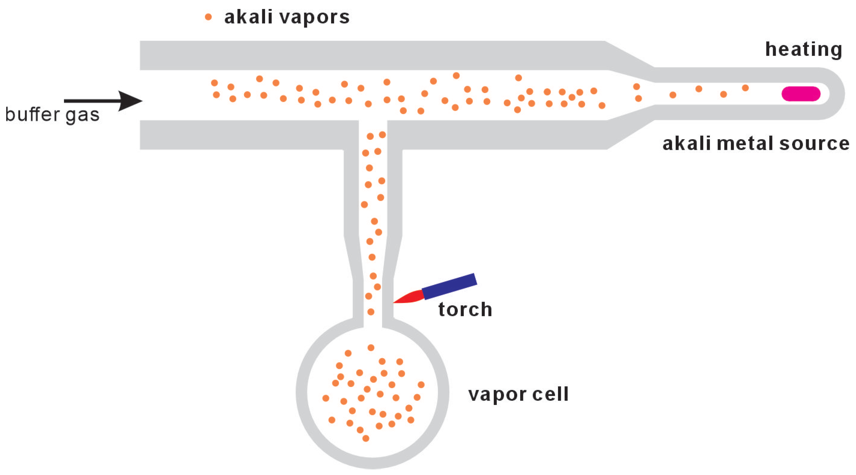
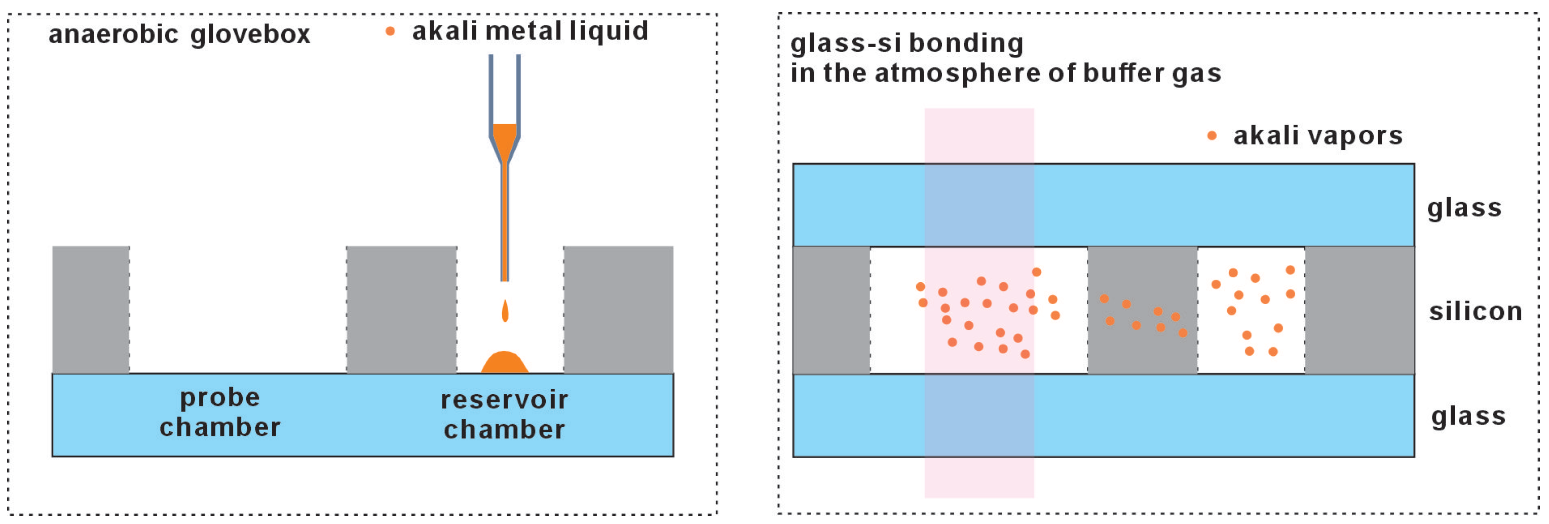
Pure Alkali Metal
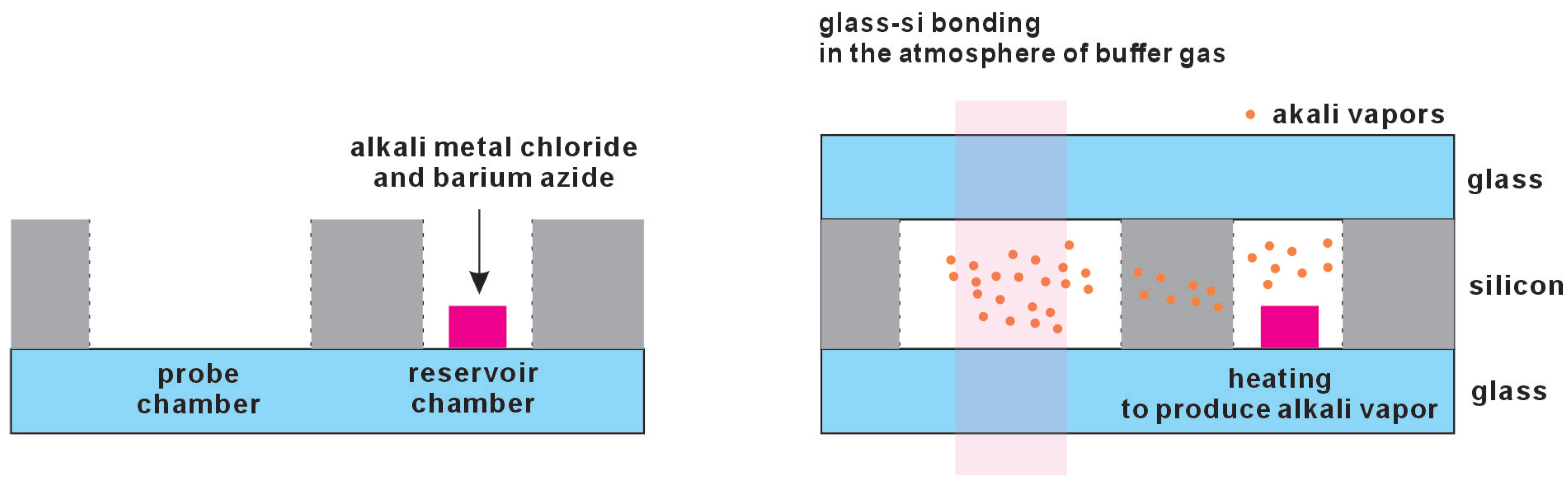
Chemical Reaction
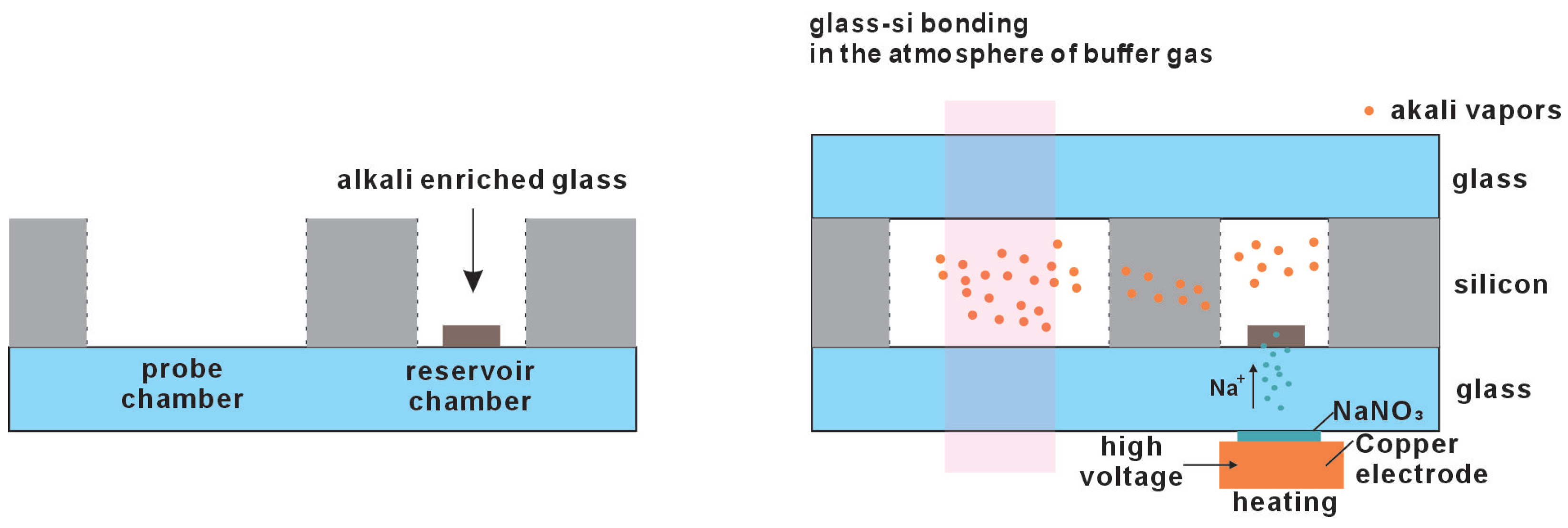
Electrolytic Alkali Metal
2.2.2. The Bonding Techniques
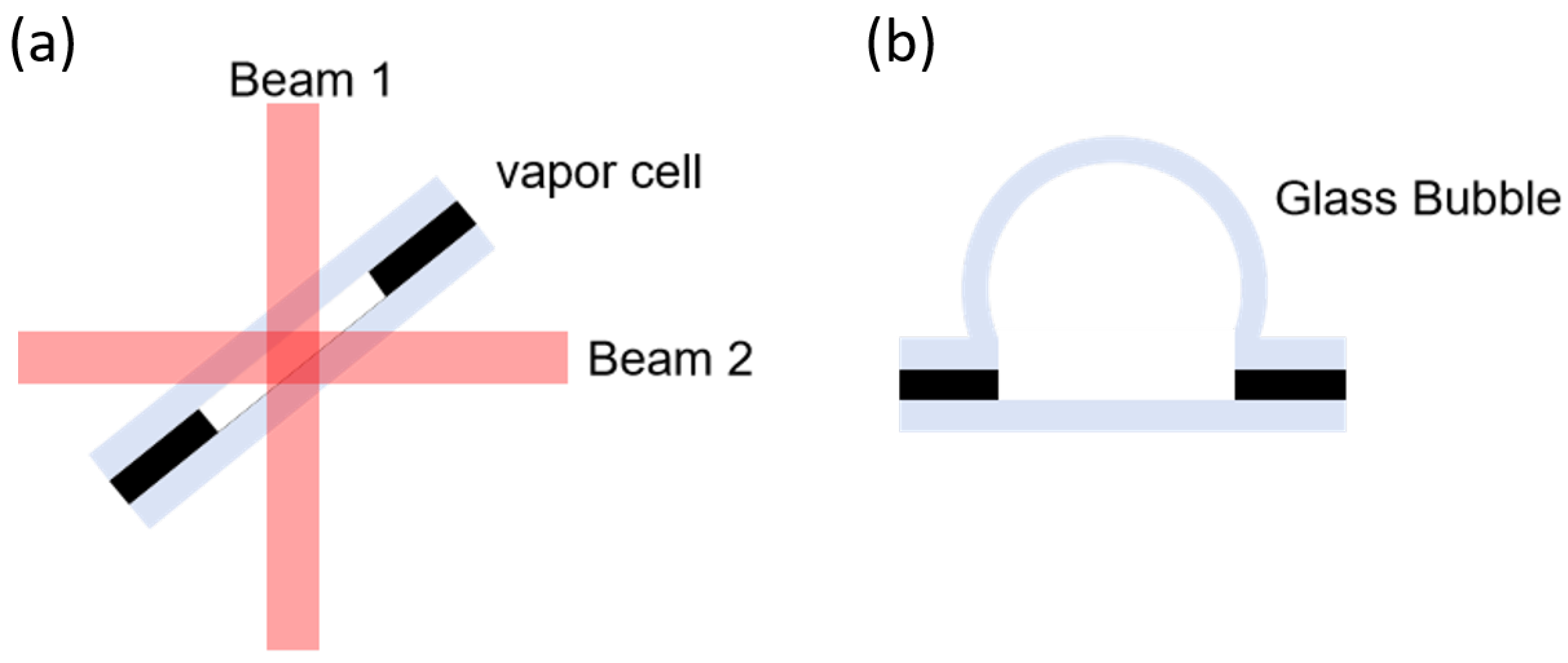
2.2.3. Cells for Dual-Beam Configurations
2.2.4. Cell Insulation
3. Lasers
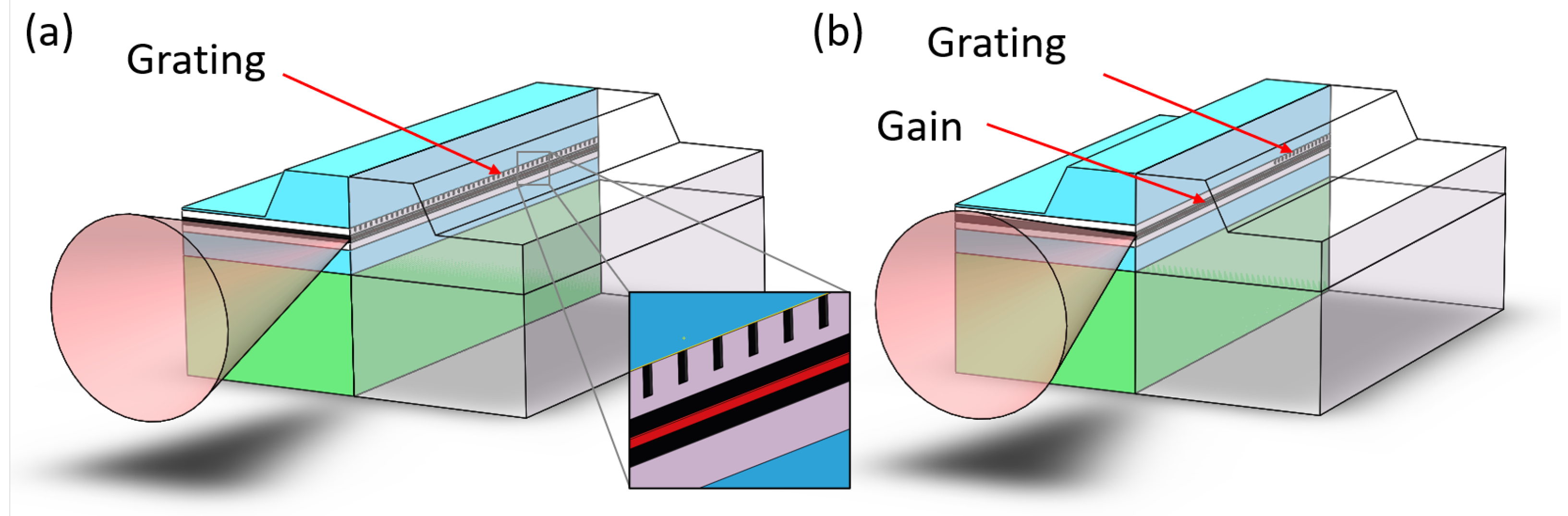
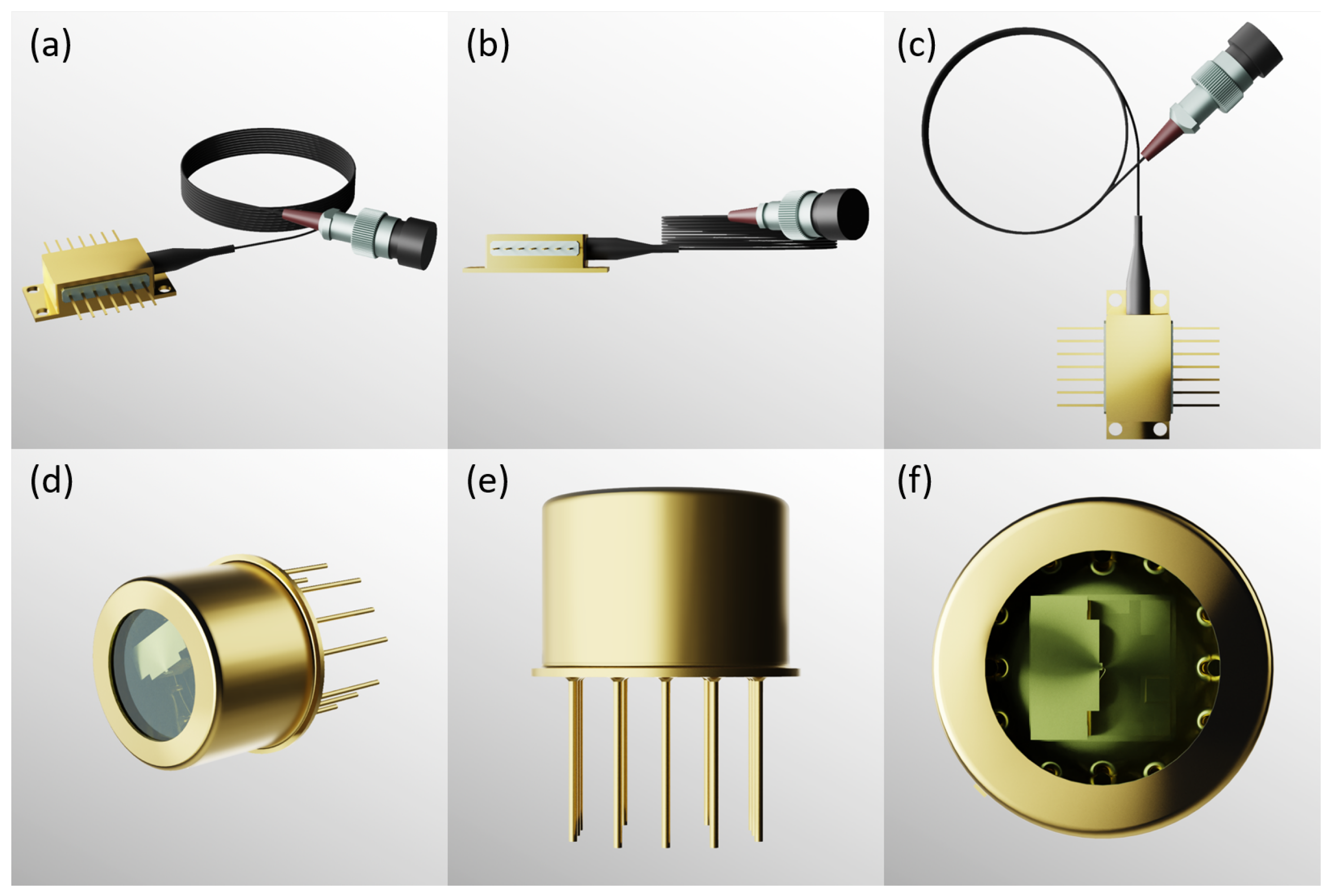
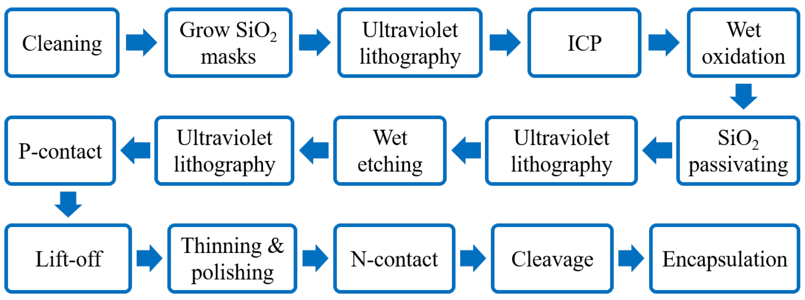
3.1. Edge-Emitting Laser Diodes
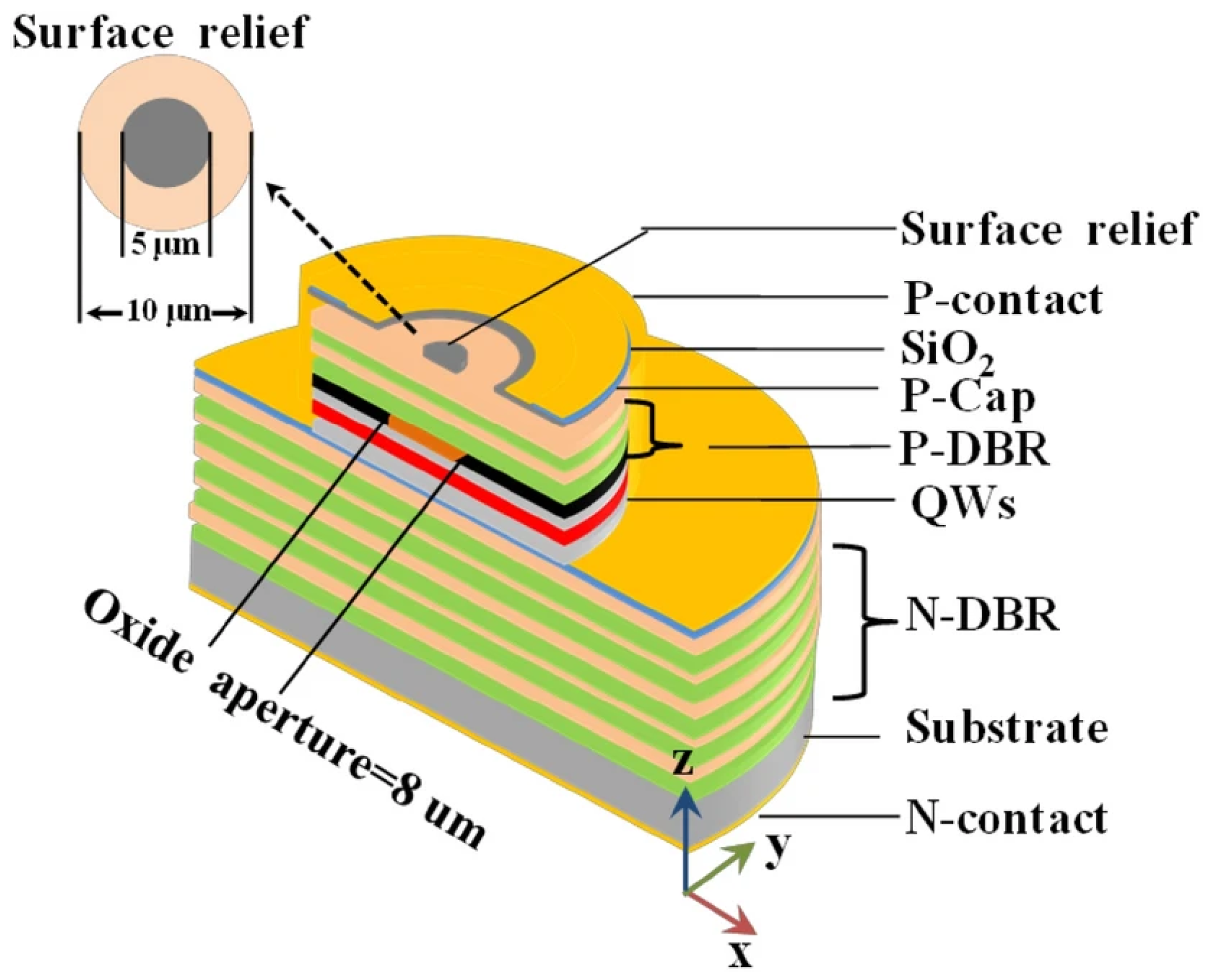
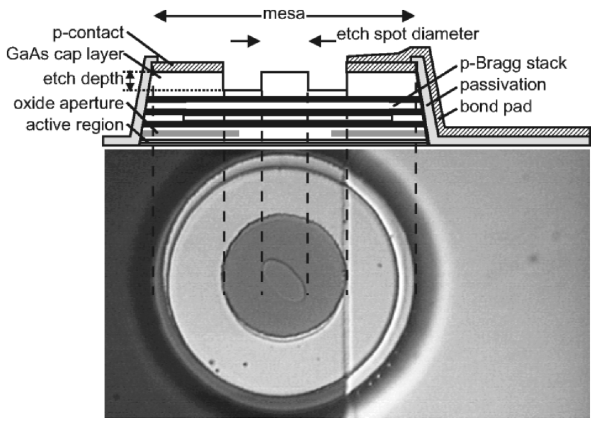
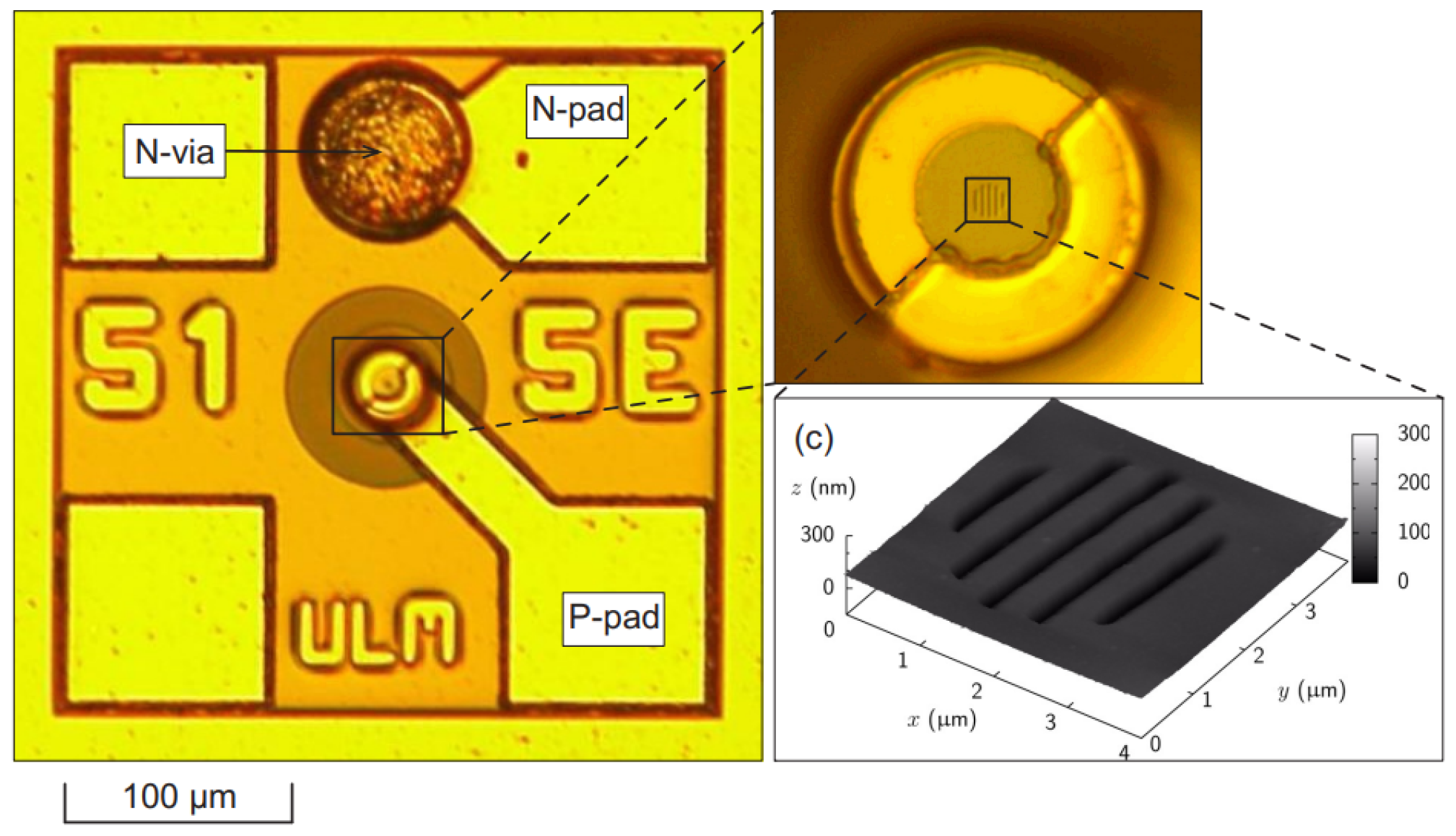
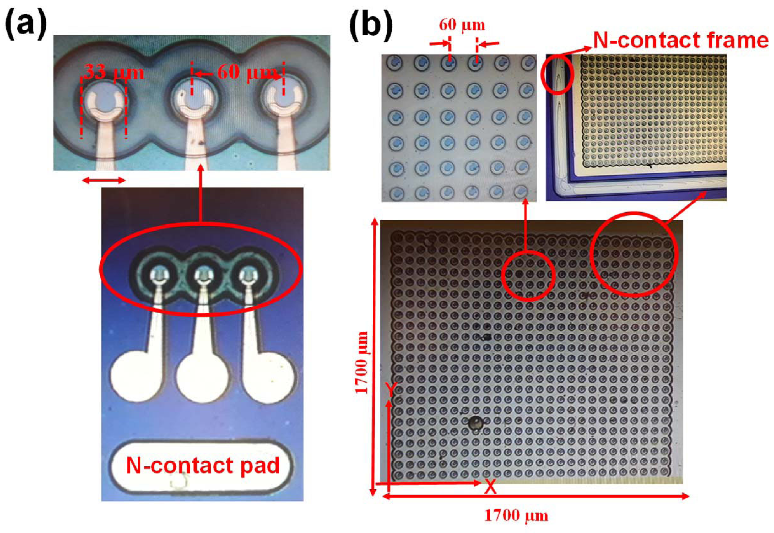
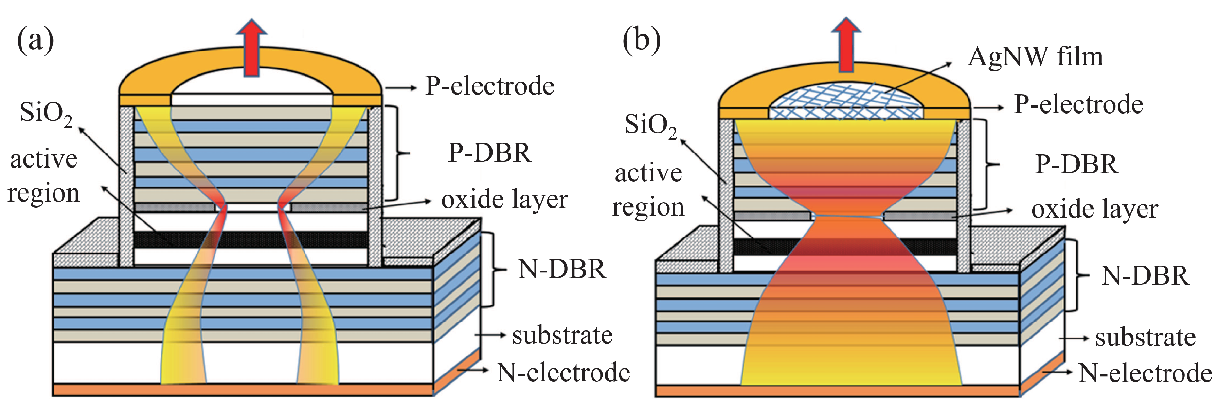
3.2. Surface-Emitting Laser Diodes
- Beam quality: VCSELs emit light from a circularly symmetric aperture, creating a spot with a small divergence angle. This symmetry facilitates simple, low-cost, and efficient coupling through basic beam shaping systems. In contrast, edge-emitting lasers produce elliptical spots with aspect ratios up to 100:1, often requiring additional beam shaping systems.
- Low threshold: The small active region in VCSELs enables low threshold lasing, potentially down to the microampere level.
- Absence of facet damage: The reflectors in VCSELs are epitaxially grown DBRs, which prevents optical damage to the laser cavity facets.
- Stability and reliability: The refractive index of the semiconductor materials used in VCSELs varies minimally with temperature changes, leading to minimal wavelength drift. Additionally, VCSELs operate effectively across a broad temperature range.
- Single-mode output: The resonant cavity length of VCSELs is very short, often just a few micrometers, with large separation between longitudinal modes. This typically results in a single longitudinal-mode output and a higher relaxation oscillation frequency.
- Large-scale two-dimensional arrays: The perpendicular emission direction of VCSELs relative to the substrate facilitates the integration of large-scale two-dimensional arrays. This alignment also removes the need for cleaving, enabling low-cost fabrication and testing, as well as high-density integration with high power output.
3.3. Potentials of VCSELs
- Optical Power
- Beam Quality
- Linewidth
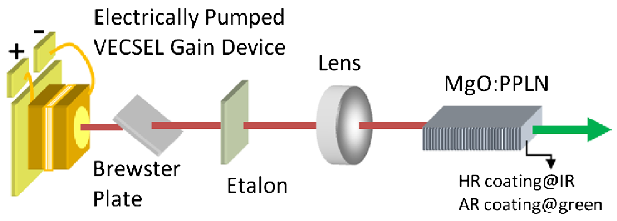
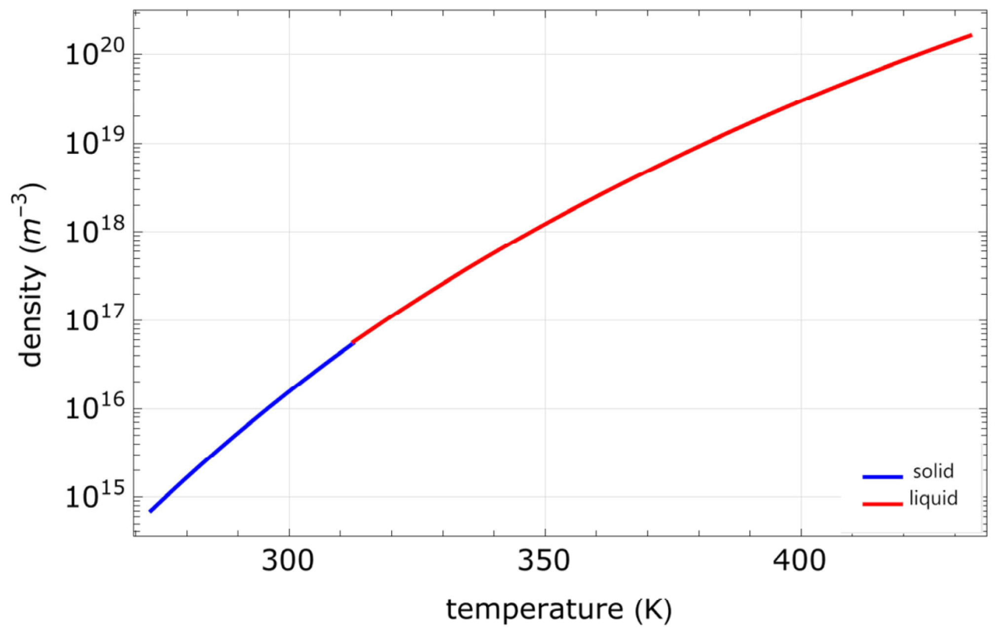
3.4. Laser Heating
3.5. Optical Elements
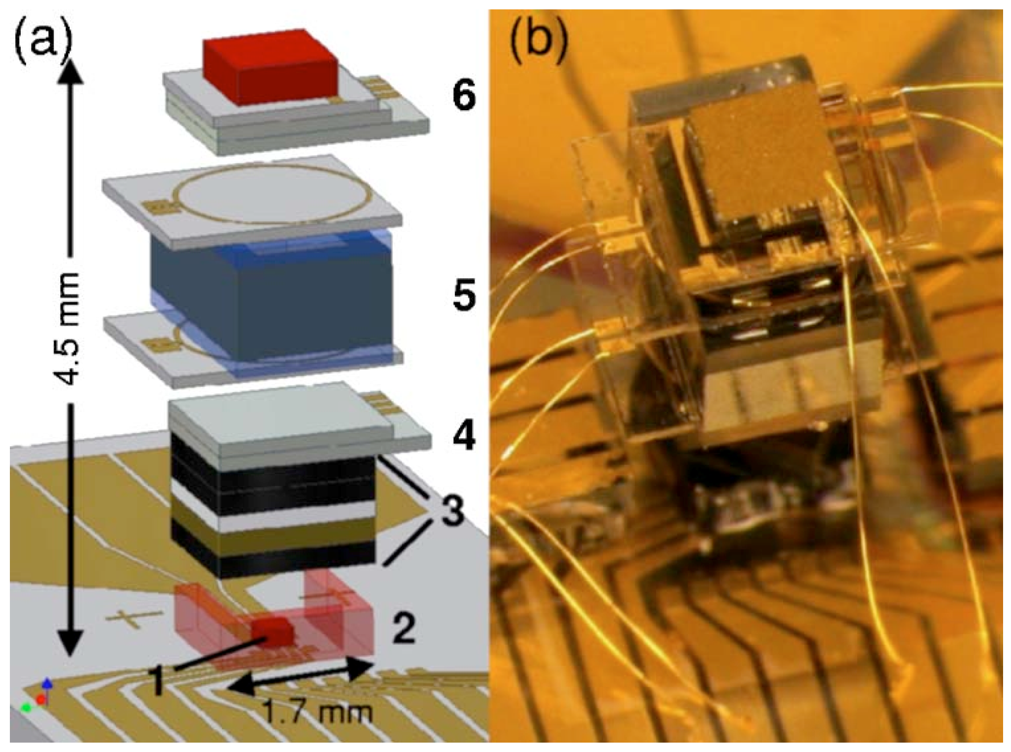
4. Coils
- Glass substrate cleaning: Take the quartz glass with a length and width of 70 mm and a thickness of 0.55 mm, clean the surface of the glass substrate with an ultrasonic cleaner and deionized water, and dry it with a drying oven.
- ITO magnetron sputtering coating: Evenly coat the cleaned glass substrate with a layer of ITO (film thickness of about 200 nm).
- Coating photoresist: The use of homogenizer in the glass coated with ITO side should be evenly coated with a layer of photoresist, photoresist model AZ1500.
- Photolithography + development + etching: The production of a good pattern mask, the use of model URE-2000/35 photolithography in the photoresist engraved with the desired pattern, with the ZX-238 positive gel developer to remove the exposed area, leaving the unexposed area, and then soaked in 20% of dilute hydrochloric acid etching is not covered by the photoresist area.
- De-gumming: The use of AZ400T de-gumming solution to remove excess photoresist.
- Point coating conductive silver glue: The use of high concentrations of quick-drying conductive silver glue connected to the upper and lower pins.
- Buckle insulation: The two pieces of surface circuitry engraved on the surface of the mutual buckle and the use of transparent insulating high-temperature double-sided tape to prevent short circuits.
- Lead electrode: from the glass surface pins with conductive silver paste lead to the positive and negative poles.
4.1. Rigid MEMS Coils
4.2. Flexible MEMS Coils
4.3. Other Types of Electric Heaters
4.4. Coils for Uniform Magnetic Fields
5. Conclusions and Discussion
Author Contributions
Funding
Conflicts of Interest
Abbreviations
| CSAC | Chip-scale atomic clock |
| DAVLL | Dichroic atomic vapor laser lock |
| DBR | Distributed Bragg reflector |
| DFB | Distributed feedback |
| FPC | Flexible printed circuits |
| ITO | Indium tin oxide |
| MEMS | Micro-electro-mechanical system |
| NMRG | Nuclear magnetic resonance gyroscope |
| OPM | Optical pump magnetometer |
| OPSR | Orthogonal polarization suppression ratio |
| PID | Proportional–integral–derivative |
| SERF | Spin-exchange relaxation-free |
| VCSEL | Vertical-cavity surface-emitting laser |
References
- Budker, D.; Romalis, M. Optical Magnetometry. Nat. Phys. 2007, 3, 227–234. [Google Scholar] [CrossRef]
- Li, J.; Quan, W.; Zhou, B.; Wang, Z.; Lu, J.; Hu, Z.; Liu, G.; Fang, J. SERF Atomic Magnetometer–Recent Advances and Applications: A Review. IEEE Sens. J. 2018, 18, 8198–8207. [Google Scholar] [CrossRef]
- Zheng, W.; Su, S.; Zhang, G.; Bi, X.; Lin, Q. Vector Magnetocardiography Measurement with a Compact Elliptically Polarized Laser-Pumped Magnetometer. Biomed. Opt. Express 2020, 11, 649. [Google Scholar] [CrossRef] [PubMed]
- Bi, X.; Ruan, L.; Liu, Z.; Li, K.; Ruan, Y.; Zheng, W.; Lin, Q. Quantitative Analysis of Magnetic Cobalt Particles with an Optically Pumped Atomic Magnetometer. Appl. Phys. Lett. 2021, 118, 084101. [Google Scholar] [CrossRef]
- Arditi, M.; Carver, T.R. Optical Detection of Zero-Field Hyperfine Splitting of Na23. Phys. Rev. 1958, 109, 1012–1013. [Google Scholar] [CrossRef]
- Bender, P.L.; Beaty, E.C.; Chi, A.R. Optical Detection of Narrow Rb87 Hyperfine Absorption Lines. Phys. Rev. Lett. 1958, 1, 311–313. [Google Scholar] [CrossRef]
- Vig, J. Military Applications of High Accuracy Frequency Standards and Clocks. IEEE Trans. Ultrason. Ferroelectr. Freq. Control 1993, 40, 522–527. [Google Scholar] [CrossRef]
- Kitching, J. Chip-Scale Atomic Devices. Appl. Phys. Rev. 2018, 5, 031302. [Google Scholar] [CrossRef]
- Kanegsberg, E. A Nuclear Magnetic Resonance (NMR) Gyro with Optical Magnetometer Detection. In Proceedings of the 22nd Annual Technical Symposium, San Diego, CA, USA, 28–31 August 1978; Ezekiel, S., Knausenberger, G.E., Eds.; SPIE: San Diego, CA, USA, 1978; pp. 73–80. [Google Scholar]
- Kornack, T.W.; Ghosh, R.K.; Romalis, M.V. Nuclear Spin Gyroscope Based on an Atomic Comagnetometer. Phys. Rev. Lett. 2005, 95, 230801. [Google Scholar] [CrossRef]
- Fang, J.; Qin, J. Advances in Atomic Gyroscopes: A View from Inertial Navigation Applications. Sensors 2012, 12, 6331–6346. [Google Scholar] [CrossRef]
- Liu, Y.; Wang, W.; Wang, X. Key Technology and Development Tendency of Micro Nuclear Magnetic Resonance Gyroscope. Navig. Control 2014, 13, 1–6. [Google Scholar]
- Fan, H.Q.; Kumar, S.; Daschner, R.; Kübler, H.; Shaffer, J.P. Subwavelength Microwave Electric-Field Imaging Using Rydberg Atoms inside Atomic Vapor Cells. Opt. Lett. 2014, 39, 3030. [Google Scholar] [CrossRef] [PubMed]
- Fan, H.; Kumar, S.; Sedlacek, J.; Kübler, H.; Karimkashi, S.; Shaffer, J.P. Atom Based RF Electric Field Sensing. J. Phys. B At. Mol. Opt. Phys. 2015, 48, 202001. [Google Scholar] [CrossRef]
- Kumar, S.; Fan, H.; Kübler, H.; Jahangiri, A.J.; Shaffer, J.P. Rydberg-Atom Based Radio-Frequency Electrometry Using Frequency Modulation Spectroscopy in Room Temperature Vapor Cells. Opt. Express 2017, 25, 8625. [Google Scholar] [CrossRef] [PubMed]
- Sedlacek, J.A.; Schwettmann, A.; Kübler, H.; Löw, R.; Pfau, T.; Shaffer, J.P. Microwave Electrometry with Rydberg Atoms in a Vapour Cell Using Bright Atomic Resonances. Nat. Phys. 2012, 8, 819–824. [Google Scholar] [CrossRef]
- Clarke, J.; Braginski, A.I. The SQUID Handbook; John Wiley & Sons, Ltd.: Hoboken, NJ, USA, 2004. [Google Scholar]
- Xue, Y. The Design and Research of Minor Fluxgate Sensor. Ph.D. Thesis, Harbin Engineering University, Harbin, China, 2010. [Google Scholar]
- Dehmel, G. Magnetic Field Sensors: Induction Coil (Search Coil) Sensors. In Sensors Set; John Wiley & Sons, Ltd.: Hoboken, NJ, USA, 1995; Chapter 6; pp. 205–253. [Google Scholar]
- Knappe, S.; Shah, V.; Schwindt, P.; Hollberg, L.; Kitching, J. A microfabricated atomic clock. Appl. Phys. Lett. 2004, 85, 1460–1462. [Google Scholar] [CrossRef]
- Knappe, S.; Schwindt, P.; Shah, V.; Hollberg, L.; Kitching, J.; Liew, L.; Moreland, J. Microfabricated atomic frequency references. In Proceedings of the the IEEE International Ultrasonics, Ferroelectrics, and Frequency Control Joint 50th Anniversary Conference, Montreal, QC, Canada, 24–27 August 2004; pp. 87–91. [Google Scholar]
- Gerginov, V.; Knappe, S.; Schwindt, P.; Shah, V.; Liew, L.; Moreland, J.; Robinson, H.; Hollberg, L.; Kitching, J.; Brannon, A. Component-level demonstration of a microfabricated atomic frequency reference. In Proceedings of the the IEEE International Frequency Control Symposium and Exposition, Vancouver, BC, Canada, 29–31 August 2005; pp. 758–766. [Google Scholar]
- Kitching, J.; Knappe, S.; Liew, L.; Schwindt, P.; Shah, V.; Moreland, J.; Hollberg, L. Microfabricated atomic clock. In Proceedings of the the 18th IEEE International Conference on Micro Electro Mechanical Systems, MEMS 2005, Miami Beach, FL, USA, 30 January–3 February 2005; pp. 1–7. [Google Scholar]
- Reference Gas Cells Portfolio and Technical Description. Available online: http://www.precisionglassblowing.com (accessed on 16 January 2024).
- Lutwak, R.; Emmons, D.; English, T.; Riley, W.; Duwel, A.; Varghese, M.; Serkland, D.; Peake, G. The chip-scale atomic clock-recent development progress. In Proceedings of the the 35th Annual Precise Time and Time Interval (PTTI) Meeting, San Diego, CA, USA, 2–4 December 2003; pp. 467–478. [Google Scholar]
- Liew, L.; Knappe, S.; Moreland, J.; Robinson, H.; Hollberg, L.; Kitching, J. Microfabricated alkali atom vapor cells. Appl. Phys. Lett. 2004, 84, 2694–2696. [Google Scholar] [CrossRef]
- Kwakernaak, M.; Lipp, S.; McBride, S.; Zanzucchi, P.; Chan, W.; Khalfin, V.; An, H.; Whaley, R.J.; Willner, B.; Ulmer, A. Components for batch-fabricated chip-scale atomic-clocks. In Proceedings of the the 36th Annual Precise Time and Time Interval (PTTI) Meeting, Washington, DC, USA, 7–9 December 2004; pp. 355–368. [Google Scholar]
- Lutwak, R.; Deng, J.; Riley, W.; Varghese, M.; Leblanc, J.; Tepolt, G.; Mescher, M.; Serkland, D.K.; Geib, K.M.; Peake, G.M. The Chip-Scale Atomic Clock—Low-Power Physics Package. In Proceedings of the the 36th Annual Precise Time and Time Interval (PTTI) Meeting, Washington, DC, USA, 7–9 December 2004; pp. 339–354. [Google Scholar]
- Lal, A.; Radhakrishnan, S. Alkali Metal-Wax Micropackets for Alkali Metal Handling. U.S. Patent 7,666,485 B2, 15 February 2007. [Google Scholar]
- Rutkowski, J. Investigation of Thermal Activation of Caesium Dispensers for Micro-Atomic Clock. Master’s Thesis, Wroclaw University of Science and Technology, Wroclaw, Poland, 2010. [Google Scholar]
- Liew, L.; Moreland, J.; Gerginov, V. Wafer-level filling of microfabricated atomic vapor cells based on thin-film deposition and photolysis of cesium azide. Appl. Phys. Lett. 2007, 90, 114106. [Google Scholar] [CrossRef]
- Karlen, S.; Gobet, J.; Overstolz, T.; Haesler, J.; Lecomte, S. Lifetime assessment of RbN3–filled MEMS atomic vapor cells with Al2O3 coating. Opt. Express 2017, 25, 2187–2194. [Google Scholar] [CrossRef]
- Gong, F.; Jau, Y.; Jensen, K.; Happer, W. Electrolytic fabrication of atomic clock cells. Rev. Sci. Instrum. 2006, 77, 076101. [Google Scholar] [CrossRef]
- Pétremand, Y.; Affolderbach, C.; Straessle, R.; Pellaton, M.; Briand, D.; Mileti, G.; de Rooij, N. Microfabricated rubidium vapous cell with a thick glass core for small-scale atomic clock applications. J. Micromech. Microeng. 2012, 22, 025013. [Google Scholar] [CrossRef]
- Dziuban, J. Bonding in Microsystem Technology; Springer: Berlin, Germany, 2006. [Google Scholar]
- Bao, H.; Duan, J.; Jin, S.; Lu, X.; Li, P.; Qu, W.; Wang, M.; Novikova, I.; Mikhailov, E.E.; Zhao, K.F.; et al. Spin squeezing of 1011 atoms by prediction and retrodiction measurements. Nature 2020, 581, 159–163. [Google Scholar] [CrossRef]
- Dideriksen, K.B.; Schmieg, R.; Zugenmaier, M.; Polzik, E.S. Room-temperature single-photon source with near-millisecond built-in memory. Nat. Commun. 2021, 12, 3699. [Google Scholar] [CrossRef]
- Zheng, W.; Wang, H.; Schmieg, R.; Oesterle, A.; Polzik, E.S. Entanglement-enhanced magnetic induction tomography. Phys. Rev. Lett. 2023, 130, 203602. [Google Scholar] [CrossRef] [PubMed]
- Seltzer, S.J.; Romalis, M.V. High-temperature alkali vapor cells with antirelaxation surface coatings. J. Appl. Phys. 2009, 106, 114905. [Google Scholar] [CrossRef]
- Karlen, S.; Haesler, J.; Overstolz, T.; Bergonzi, G.; Lecomte, S. MEMS atomic vapor cells sealed by Cu-Cu thermocompression bonding. In Proceedings of the 2017 Joint Conference of the European Frequency and Time Forum and IEEE International Frequency Control Symposium (EFTF/IFCS), Besancon, France, 9–13 July 2017; pp. 625–627. [Google Scholar]
- Rushton, J.; Aldous, M.; Himsworth, M. The feasibility of a fully miniaturized magneto-optical trap for portable ultracold quantum technology. Rev. Sci. Instrum. 2014, 85, 121501. [Google Scholar] [CrossRef] [PubMed]
- Straessle, R.; Pellaton, M.; Affolderbach, C.; Pétremand, Y.; Briand, D.; Mileti, G.; de Rooij, N.F. Microfabricated alkali vapor cell with anti-relaxation wall coating. Appl. Phys. Lett. 2014, 105, 043502. [Google Scholar] [CrossRef]
- Vecchio, F.; Venkatraman, V.; Shea, H.R.; Maeder, T.; Ryser, P. Dispensing and hermetic sealing Rb in a miniature reference cell for integrated atomic clocks. Sens. Actuators A Phys. 2011, 172, 330–335. [Google Scholar] [CrossRef]
- Gardner, A.T.; Collins, J.A. A second look at Chip Scale Atomic Clocks for long term precision timing. In Proceedings of the OCEANS 2016 MTS/IEEE Monterey, Monterey, CA, USA, 19–23 September 2016; pp. 1–9. [Google Scholar]
- Griffith, W.C.; Knappe, S.; Kitching, J. Femtotesla atomic magnetometry in a microfabricated vapor cell. Opt. Express 2010, 18, 27167–27172. [Google Scholar] [CrossRef]
- Eklund, E.J.; Shkel, A.M.; Knappe, S.; Donley, E.; Kitching, J. Glass-Blown Spherical Microcells for Chip-Scale Atomic Devices. Sens. Actuators A Phys. 2008, 143, 175–180. [Google Scholar] [CrossRef]
- Kogelnik, H.; Shank, C.V. Stimulated Emission in a Periodic Structure. Appl. Phys. Lett. 1971, 18, 152–154. [Google Scholar] [CrossRef]
- Photodigm DBR Laser Diodes ranging 730–1100 nm. Available online: https://www.photodigm.com/ (accessed on 29 July 2024).
- Soda, H.; Iga, K.i.; Kitahara, C.; Suematsu, Y. GaInAsP/InP Surface Emitting Injection Lasers. Jpn. J. Appl. Phys. 1979, 18, 2329–2330. [Google Scholar] [CrossRef]
- Hua, L.; Yang, Y. Characteristics and Developmentof Optically Pumped Vertical External Cavity Surface Emitting Lasers. Mater. Rev. 2013, 27, 64–69. [Google Scholar]
- Paranthoen, C.; Levallois, C.; Brevalle, G.; Perrin, M.; Le Corre, A.; Chevalier, N.; Turban, P.; Cornet, C.; Folliot, H.; Alouini, M. Low Threshold 1550-nm Emitting QD Optically Pumped VCSEL. IEEE Photonics Technol. Lett. 2021, 33, 69–72. [Google Scholar] [CrossRef]
- Li, X.; Zhou, Y.; Zhang, X.; Zhang, J.; Zeng, Y.; Ning, Y.; Wang, L. High-Power Single-Mode 894 nm VCSELs Operating at High Temperature (>2 mW @ 365 K). Appl. Phys. B 2022, 128, 16. [Google Scholar]
- Iga, K.; Koyama, F.; Kinoshita, S. Surface Emitting Semiconductor Lasers. IEEE J. Quantum Electron. 1988, 24, 1845–1855. [Google Scholar] [CrossRef]
- Iga, K. Surface-Emitting Laser-Its Birth and Generation of New Optoelectronics Field. IEEE J. Sel. Top. Quantum Electron. 2000, 6, 1201–1215. [Google Scholar] [CrossRef]
- Zhang, J.; Li, X.; Zhang, J.; Ning, Y.; Wang, L. Research Progress of Vertical-cavity Surface-emitting Laser. Chin. J. Lumin. 2020, 41, 1443–1459. [Google Scholar] [CrossRef]
- Zhou, Y.; Jia, Y.; Zhang, X.; Zhang, J.; Liu, Z.; Ning, Y.; Wang, L. Large-Aperture Single-Mode 795 nm VCSEL for Chip-Scale Nuclear Magnetic Resonance Gyroscope with an Output Power of 4.1 mW at 80 °C. Opt. Express 2022, 30, 8991. [Google Scholar] [CrossRef]
- Yan, G.; Hao, Y. High Beam Quality High Power Vertical Cavity Surface Emitting Lasers. Chin. J. Lasers 2024, 51, 1101001. [Google Scholar]
- Kitching, J.; Knappe, S.; Vukicevic, M.; Hollberg, L.; Wynands, R.; Weidmann, W. A Microwave Frequency Reference Based on VCSEL-driven Dark Line Resonances in Cs Vapor. IEEE Trans. Instrum. Meas. 2000, 49, 1313–1317. [Google Scholar] [CrossRef]
- Schwindt, P.D.D.; Lindseth, B.; Knappe, S.; Shah, V.; Kitching, J.; Liew, L.A. Chip-Scale Atomic Magnetometer with Improved Sensitivity by Use of the Mx Technique. Appl. Phys. Lett. 2007, 90, 081102. [Google Scholar] [CrossRef]
- Debernardi, P.; Unold, H.; Maehnss, J.; Michalzik, R.; Bava, G.; Ebeling, K. Single-Mode, Single-Polarization VCSELs via Elliptical Surface Etching: Experiments and Theory. IEEE J. Sel. Top. Quantum Electron. 2003, 9, 1394–1404. [Google Scholar] [CrossRef]
- Ostermann, J.; Debernardi, P.; Jalics, C.; Michalzik, R. Polarization-Stable Oxide-Confined VCSELs with Enhanced Single-Mode Output Power via Monolithically Integrated Inverted Grating Reliefs. IEEE J. Sel. Top. Quantum Electron. 2005, 11, 982–989. [Google Scholar] [CrossRef]
- Wahl, D.; Setz, D.S.; Al-Samaneh, A. Development of VCSELs for Atomic Clock Applications; Technical Report; Institute of Optoelectronics, Ulm University: Ulm, Germany, 2008. [Google Scholar]
- Al-Samaneh, A. VCSELs for Atomic Clock Demonstrators; Technical Report; Institute of Optoelectronics, Ulm University: Ulm, Germany, 2013. [Google Scholar]
- Keeler, G.A.; Geib, K.M.; Serkland, D.K.; Peake, G.M.; Wendt, J.R. VCSEL Polarization Control for Chip-Scale Atomic Clocks; Technical Report; Sandia National Laboratories: Albuquerque, NM, USA, 2007. [Google Scholar]
- Derebezov, I.A.; Haisler, V.A.; Bakarov, A.K.; Kalagin, A.K.; Toropov, A.I.; Kachanova, M.M.; Gavrilova, T.A.; Medvedev, A.S.; Nenasheva, L.A.; Shayakhmetov, V.M.; et al. Single-Mode Vertical-Cavity Surface-Emitting Lasers for Atomic Clocks. Optoelectron. Instrum. Data Process. 2009, 45, 361–366. [Google Scholar] [CrossRef]
- Maleev, N.A.; Blokhin, S.A.; Bobrov, M.A.; Kuz’menkov, A.G.; Kulagina, M.M.; Ustinov, V.M. Laser Source for a Compact Nuclear Magnetic Resonance Gyroscope. Gyroscopy Navig. 2018, 9, 177–182. [Google Scholar] [CrossRef]
- Zhao, J.; Qin, L.; Yan, S.; Ren, X. Design of VCSEL Laser Control System Based on CPT Atomic Clock. Electron. Des. Eng. 2009, 17, 118–119. [Google Scholar]
- Gruet, F.; Al-Samaneh, A.; Kroemer, E.; Bimboes, L.; Miletic, D.; Affolderbach, C.; Wahl, D.; Boudot, R.; Mileti, G.; Michalzik, R. Metrological Characterization of Custom-Designed 894.6 nm VCSELs for Miniature Atomic Clocks. Opt. Express 2013, 21, 5781. [Google Scholar] [CrossRef]
- Watkins, L.S.; Ghosh, C.; Seurin, J.F.; Zhou, D.; Xu, G.; Xu, B.; Miglo, A. High Power VCSEL Devices for Atomic Clock Applications. In Proceedings of the SPIE Optical Engineering + Applications, San Diego, CA, USA, 11–13 August 2015; Taylor, E.W., Cardimona, D.A., Eds.; SPIE: San Diego, CA, USA, 2015; p. 96160J. [Google Scholar]
- Zaouris, D.; Powell, D.; Knapp, M.; Haji, M.; Gill, P.; Shutts, S.; Smowton, P.M.; Eddie, I.; McKee, A.; Meredith, W. MacV: VCSELs For Miniature Atomic Clocks. In Proceedings of the 2019 Joint Conference of the IEEE International Frequency Control Symposium and European Frequency and Time Forum (EFTF/IFC), Orlando, FL, USA, 14–18 April 2019; IEEE: Orlando, FL, USA, 2019; pp. 1–2. [Google Scholar]
- Pang, W.; Pan, G.; Wang, Q.; Hu, L.; Zhao, Z.; Xie, Y. 894.6 nm VCSEL for Cs-Based Atomic Clocks with Triangular Holey Structure. In Proceedings of the 2020 3rd International Conference on Electron Device and Mechanical Engineering (ICEDME), Suzhou, China, 1–3 May 2020; IEEE: Suzhou, China, 2020; pp. 573–575. [Google Scholar]
- Zhang, J.; Ning, Y.; Zeng, Y.; Zhang, J.; Zhang, J.; Fu, X.; Tong, C.; Wang, L. Design and Analysis of High-Temperature Operating 795 nm VCSELs for Chip-Scale Atomic Clocks. Laser Phys. Lett. 2013, 10, 045802. [Google Scholar]
- Zhang, J.; Ning, Y.; Zhang, J.; Zhang, X.; Zeng, Y.; Wang, L. 795 nm VCSELs for 87Rb Based Miniaturized Atomic Clock. Opt. Precis. Eng. 2014, 22, 50–57. [Google Scholar] [CrossRef]
- Zhang, J.; Zhang, X.; Zhu, H.; Zhang, J.; Ning, Y.; Qin, L.; Wang, L. High-Temperature Operating 894.6 nm-VCSELs with Extremely Low Threshold for Cs-based Chip Scale Atomic Clocks. Opt. Express 2015, 23, 14763. [Google Scholar] [CrossRef]
- Xiang, L.; Zhang, X.; Zhang, J.W.; Ning, Y.Q.; Hofmann, W.; Wang, L.J. Stable Single-Mode Operation of 894.6 Nm VCSEL at High Temperatures for Cs Atomic Sensing. Chin. Phys. B 2017, 26, 074209. [Google Scholar] [CrossRef]
- Liu, Y.; Zhang, X.; Huang, Y.; Zhang, J.; Hofmann, W.; Ning, Y.; Wang, L. OPSR Enhancement of High-Temperature Operating Shallow-Surface Grating VCSELs. Appl. Opt. 2018, 57, 4486. [Google Scholar] [CrossRef]
- Zhang, R.; Hanselmann, F.; Fochs, R.; Lawrence, M.; Hurley, K.; Prouty, M. Motion Noise Reduction in Drone Magnetometry Using a Dead-Zone-Free Total-Field Magnetometer System. Lead. Edge 2022, 41, 481–485. [Google Scholar] [CrossRef]
- Zhang, C.; Li, S.; Zhao, Q.; Shu, S.; Wu, Z.; Liu, H. VCSEL Frequency Stabilization Research for Dual-cell Cs Optical Pumping Magnetometer. Laser J. 2023, 1, 1. [Google Scholar]
- QuSpin, Inc. Available online: http://www.quspin.com (accessed on 29 July 2024).
- Beijing X-MAGTECH Technologies. Available online: https://www.xmagtech.com/ (accessed on 29 July 2024).
- Miller, M.; Grabherr, M.; King, R.; Jager, R.; Michalzik, R.; Ebeling, K. Improved Output Performance of High-Power VCSELs. IEEE J. Sel. Top. Quantum Electron. 2001, 7, 210–216. [Google Scholar] [CrossRef]
- Li, T.; Ning, Y.; Sun, Y.; Wang, C.; Liu, J.; Liu, Y.; Wang, L. High-Power InGaAs VCSEL’s Single Devices and 2-D Arrays. J. Lumin. 2007, 122–123, 571–573. [Google Scholar] [CrossRef]
- D’Asaro, L.A.; Seurin, J.F.; Wynn, J.D. High-power, High-efficiency VCSELs Pursue the Goal. Photonics Spectra 2005, 39, 62–66. [Google Scholar]
- Seurin, J.F.; Ghosh, C.L.; Khalfin, V.; Miglo, A.; Xu, G.; Wynn, J.D.; Pradhan, P.; D’Asaro, L.A. High-Power High-Efficiency 2D VCSEL Arrays. In Proceedings of the Integrated Optoelectronic Devices, San Jose, CA, USA, 29 January 2008; Lei, C., Guenter, J.K., Eds.; SPIE: San Jose, CA, USA, 2008; p. 690808. [Google Scholar]
- Seurin, J.F.; Ghosh, C.L.; Khalfin, V.; Miglo, A.; Xu, G.; Wynn, J.D.; Pradhan, P.; D’Asaro, L.A. High-Power Vertical-Cavity Surface-Emitting Arrays. In Proceedings of the Lasers and Applications in Science and Engineering, San Jose, CA, USA, 7 February 2008; Zediker, M.S., Ed.; SPIE: San Jose, CA, USA, 2008; p. 68760D. [Google Scholar]
- Herper, M.; Lee, A.; Kolb, J.; Gronenborn, S.; Moench, H.; Loosen, P. VCSEL Pumped VECSEL Concept with Compact Design. Electron. Lett. 2019, 55, 705–707. [Google Scholar] [CrossRef]
- Zhang, L.; Ning, Y.; Zeng, Y.; Qin, L.; Liu, Y.; Zhang, X.; Liu, D.; Xu, H.; Zhang, J.; Wang, L. High-Power Bottom-Emitting Vertical-Cavity Surface-Emitting Lasers under Continuous-Wave, Quasi-Continuous-Wave, and Pulsed Operation. Appl. Phys. Express 2011, 4, 052102. [Google Scholar] [CrossRef]
- Zhang, J.; Ning, Y.; Zhang, X.; Zhang, J.; Zeng, Y.; Shan, X.; Qin, L.; Wang, L. High-Peak-Power Vertical-Cavity Surface-Emitting Laser Quasi-Array Realized Using Optimized Large-Aperture Single Emitters. Jpn. J. Appl. Phys. 2014, 53, 070303. [Google Scholar] [CrossRef]
- Khan, Z.; Shih, J.C.; Chao, R.L.; Tsai, T.L.; Wang, H.C.; Fan, G.W.; Lin, Y.C.; Shi, J.W. High-Brightness and High-Speed Vertical-Cavity Surface-Emitting Laser Arrays. Optica 2020, 7, 267. [Google Scholar] [CrossRef]
- Khan, Z.; Wu, M.L.; Lin, C.W.; Chen, C.C.; Chang, C.J.; Lu, T.C.; Ledentsov, N.; Ledentsov, N.; Shi, J.W. Miniaturized Vertical-Cavity Surface-Emitting Laser Array with a Novel Electrode Design for High-Speed, Low-Noise, and High-Brightness Performance. Adv. Photonics Res. 2023, 4, 2300072. [Google Scholar] [CrossRef]
- Guo, X.; Shi, L.; Li, C.; Dong, J.; Liu, B.; Hu, S.; He, Y. Research of the Use of Silver Nanowires as a Current Spreading Layer on Vertical-Cavity Surface-Emitting Lasers. Chin. Phys. B 2016, 25, 114208. [Google Scholar] [CrossRef]
- Hassan, A.M.A.; Gu, X.; Nakahama, M.; Shinada, S.; Ahmed, M.; Koyama, F. High Power Surface Grating Slow-Light VCSEL. Appl. Phys. Express 2021, 14, 092006. [Google Scholar] [CrossRef]
- Hassan, A.M.A.; Gu, X.; Nakahama, M.; Shinada, S.; Ahmed, M.; Koyama, F. High-Power Operations of Single-Mode Surface Grating Long Oxide Aperture VCSELs. Appl. Phys. Lett. 2021, 119, 191103. [Google Scholar] [CrossRef]
- Hu, S.; Hassan, A.; Gu, X.; Nakahama, M.; Koyama, F. Surface Grating Loaded VCSEL with Single Mode Power of over 80 mW. IEICE Electron. Express 2021, 18, 20210202. [Google Scholar] [CrossRef]
- Pan, Z.; Li, W.; Qi, Y.; Lv, J.; Liu, S.; Zhong, L.; Ma, X. Design and Analysis of Photonic Crystal Vertical-Cavity Surface-Emitting Lasers. Acta Opt. Sin. 2022, 42, 1414002. [Google Scholar]
- Wang, X.; Cui, B.; Li, C.; Xu, J.; Wang, H. Research Progress of Transverse Mode Control for Vertical Cavity Surface Emitting Lasers. Laser Optoelectron. Prog. 2021, 58, 0700008. [Google Scholar] [CrossRef]
- Yoshida, M.; De Zoysa, M.; Ishizaki, K.; Tanaka, Y.; Kawasaki, M.; Hatsuda, R.; Song, B.; Gelleta, J.; Noda, S. Double-Lattice Photonic-Crystal Resonators Enabling High-Brightness Semiconductor Lasers with Symmetric Narrow-Divergence Beams. Nat. Mater. 2019, 18, 121–128. [Google Scholar] [CrossRef] [PubMed]
- Hirose, K.; Liang, Y.; Kurosaka, Y.; Watanabe, A.; Sugiyama, T.; Noda, S. Watt-Class High-Power, High-Beam-Quality Photonic-Crystal Lasers. Nat. Photonics 2014, 8, 406–411. [Google Scholar] [CrossRef]
- Li, Y.; Zong, N.; Peng, Q. Characteristics and Progress of Vertical-Cavity Surface-Emitting Semiconductor Lasers. Laser Optoelectron. Prog. 2018, 55, 050006. [Google Scholar]
- Zhao, P.; Xu, B.; Van Leeuwen, R.; Chen, T.; Watkins, L.; Zhou, D.; Gao, P.; Xu, G.; Wang, Q.; Ghosh, C. Compact 4.7 W, 18.3% Wall-Plug Efficiency Green Laser Based on an Electrically Pumped VECSEL Using Intracavity Frequency Doubling. Opt. Lett. 2014, 39, 4766. [Google Scholar] [CrossRef] [PubMed]
- Yang, L.; Li, G.; Gao, X.; Lu, L. Topological-Cavity Surface-Emitting Laser. Nat. Photonics 2022, 16, 279–283. [Google Scholar] [CrossRef]
- Jiang, L. Study on Linewidth Narrowing and Polarization Control of Vertical-Cavity Surface-Emitting Lasers. Ph.D. Thesis, Chongqing University, Chongqing, China, 2022. [Google Scholar]
- Lv, J.; Li, W.; Qi, Y.; Pan, Z.; Zhong, L.; Liu, S.; Ma, X. Optimized Design of Support Structure for Tunable Vertical-Cavity Surface-Emitting Lasers. Acta Opt. Sin. 2023, 43, 0114003. [Google Scholar]
- II-VI Laser Enterprise. Available online: http://www.laserenterprise.com (accessed on 4 June 2024).
- Vixar Co. Available online: https://vixarinc.com (accessed on 4 June 2024).
- Wang, K.; Zhou, B.; Tang, J.; Zhang, S.; Wang, Y. Advances in laser heating of alkali vapor cells in magnetometers: A review. In Proceedings of the AOPC 2020: Optical Spectroscopy and Imaging; and Biomedical Optics, Beijing, China, 5 November 2020; Volume 11566, pp. 182–186. [Google Scholar]
- Preusser, J.; Gerginov, V.; Knappe, S.; Kitching, J. A Microfabricated Photonic Magnetometer. In Proceedings of the IEEE Sensors, Lecce, Italy, 26–29 October 2008; IEEE: Lecce, Italy, 2008; pp. 344–346. [Google Scholar]
- Mhaskar, R.; Knappe, S.; Kitching, J. A Low-Power, High-Sensitivity Micromachined Optical Magnetometer. Appl. Phys. Lett. 2012, 101, 241105. [Google Scholar] [CrossRef]
- Savukov, I.; Boshier, M. A High-Sensitivity Tunable Two-Beam Fiber-Coupled High-Density Magnetometer with Laser Heating. Sensors 2016, 16, 1691. [Google Scholar] [CrossRef]
- Li, Y.; Zhou, G.; Tian, S.; Liu, X.; Dong, X.; Gao, X. Laser Heating Method for an Alkali Metal Atomic Cell with Heat Transfer Enhancement. Photonics 2023, 10, 637. [Google Scholar] [CrossRef]
- Bai, L.; Wen, X.; Yang, Y.; Zhang, L.; He, J.; Wang, Y.; Wang, J. Quantum-enhanced rubidium atomic magnetometer based on Faraday rotation via 795 nm stokes operator squeezed light. J. Opt. 2021, 23, 085202. [Google Scholar] [CrossRef]
- Li, J.; Zheng, J.; Pan, S.; Li, K.; Yu, H.; Zheng, W. Metasurface-Based Optical System for Miniaturization of Atomic Magnetometers. Opt. Express 2024, 32, 20538. [Google Scholar] [CrossRef]
- Alcock, C.B.; Itkin, V.P.; Horrigan, M.K. Vapour Pressure Equations for the Metallic Elements: 298–2500K. Can. Metall. Q. 1984, 23, 309–313. [Google Scholar] [CrossRef]
- Di Domenico, G.; Weis, A. “Vapor Pressure and Density of Alkali Metals” from the Wolfram Demonstrations Project. Available online: http://demonstrations.wolfram.com/VaporPressureAndDensityOfAlkaliMetals/ (accessed on 24 March 2024).
- Lu, J.; Qian, Z.; Fang, J. Review of SERF Atomic Magnetometer Vapor Cell Heating Technique. In Proceedings of the 13th Sensors and Transducers Conference of China, Maoming, China, 14–16 August 2014; National Defense Industry Press: Taiyuan, China, 2014; pp. 744–747. [Google Scholar]
- Eklund, E.J. Microgyroscope Based on Spin-Polarized Nuclei. Ph.D. Thesis, University of California, Irvine, CA, USA, 2008. [Google Scholar]
- Liu, K. Research on the Weak Magnetic Measurement and Noise Reduction of Chip-Scale Atomic Magnetometer. Master’s Thesis, Southeast University, Nanjing, China, 2021. [Google Scholar]
- Chen, C. Research on The Transparent and Weak Magnetic Heating System of Atomic Magnetometer. Master’s Thesis, Zhejiang University of Technology, Hangzhou, China, 2024. [Google Scholar]
- Johnson, C.; Schwindt, P.D. A Two-Color Pump Probe Atomic Magnetometer for Magnetoencephalography. In Proceedings of the 2010 IEEE International Frequency Control Symposium, Newport Beach, CA, USA, 1–4 June 2010; IEEE: Newport Beach, CA, USA, 2010; pp. 371–375. [Google Scholar]
- Wu, L.; Gan, Q.; Ji, Y.; Shang, J. Fabrication of Wafer-Level Micro Silicon Heaters for Chip Scale Atomic Magnetometers. In Proceedings of the 2015 16th International Conference on Electronic Packaging Technology (ICEPT), Changsha, China, 11–14 August 2015; IEEE: Changsha, China, 2015; pp. 943–946. [Google Scholar]
- Liu, Z.; Li, K.; Li, Y.; Hu, X.; Yan, S.; Zhang, Y. Design of the Digital Temperature Control System for the Chip Scale Atomic Clock MEMS Atomic Vapor Cell. Semicond. Integr. Circuits 2019, 44, 410–420. [Google Scholar]
- Guo, Q.; Li, Z.; Zhao, R.; Wen, H.; Guo, H.; Tang, J.; Liu, J. Design and Realization of a Weak Magnetic Fast Electric Heating Chip. Jpn. J. Appl. Phys. 2021, 60, 066502. [Google Scholar] [CrossRef]
- Kazakin, A.; Enns, Y.; Ermak, S. MEMS Low-Magnetic Electric Heating Chip for Temperature Control of Alkali Vapor Cell. In Proceedings of the 2023 International Conference on Electrical Engineering and Photonics (EExPolytech), St. Petersburg, Russia, 19–20 October 2023; IEEE: St. Petersburg, Russia, 2023; pp. 57–60. [Google Scholar]
- Zhang, P.; Chen, H.; Gui, Y.; Sun, L.; Shao, Z.; Cui, H. Non-magnetic Temperature Control Technology of Atomic Vapor Cell in Atomic Magnetic Sensors. Transducer Microsyst. Technol. 2017, 36, 18–25. [Google Scholar]
- Wylie, R. The Development of a Multichannel Atomic Magnetometer Array for Fetal Magnetocardiography. Ph.D. Thesis, The University of Wisconsin-Madison, Madison, WI, USA, 2012. [Google Scholar]
- Liang, X.; Zhou, X.; Fang, J.; Hu, D.; Wu, W.; Jia, Y.; Liu, Z. A Quadra-Layered Multipole Moment Heating Film With Self-Cancellation of Magnetic Field. IEEE Trans. Magn. 2020, 56, 1–11. [Google Scholar] [CrossRef]
- Hao, J.; Zhou, b. Study on Non-magnetic Heating Technology and System for Alkali Vapor Cells. Comput. Meas. Control 2017, 25, 180–183. [Google Scholar]
- Yim, S.H.; Kim, Z.; Lee, S.; Kim, T.H.; Shim, K.M. Note: Double-layered Polyimide Film Heater with Low Magnetic Field Generation. Rev. Sci. Instrum. 2018, 89, 116102. [Google Scholar] [CrossRef]
- Keller, J. AOSense to Develop Navigation Chip That Combines Solid-state and Atomic Inertial Sensors. Available online: https://www.militaryaerospace.com/uncrewed/article/16715892/aosense-to-develop-navigation-chip-that-combines-solid-state-and-atomic-inertial-sensors (accessed on 14 March 2021).
- Noor, R.M.; Shkel, A.M. MEMS Components for NMR Atomic Sensors. J. Microelectromech. Syst. 2018, 27, 1148–1159. [Google Scholar] [CrossRef]
- Li, G.; Shang, J.; Zhang, J.; Ji, Y. Wafer-Level Integration of Micro Heaters on an Alkali Vapor Cell for Chip-Scale Atomic Magnetometers. In Proceedings of the 2018 19th International Conference on Electronic Packaging Technology (ICEPT), Shanghai, China, 8–11 August 2018; IEEE: Shanghai, China, 2018; pp. 1564–1567. [Google Scholar]
- Wang, Z.; Wu, J.; Zhang, J.; Shang, J. On-Chip Heating Noise Suppression of 3d Chip-Scale Atomic Magnetometer Using Single-Layer Shifted Heater. In Proceedings of the 2023 IEEE 36th International Conference on Micro Electro Mechanical Systems (MEMS), Munich, Germany, 15–19 January 2023; IEEE: Munich, Germany, 2023; pp. 546–549. [Google Scholar]
- Xie, Y.; Cheng, Z.; Li, X.; Wang, L.; Zhang, F. Non-magnetic Thermostat Control System for Cesium Optical-pumping Magnetometer. J. Astronaut. Metrol. Meas. 2022, 42, 69–72. [Google Scholar]
- Liang, S.; Wang, B.; Zhu, M.; Deng, D. Design and Simulation of Non-magnetic Heating Coils for a Miniature Nuclear Magnetic Resonance Gyroscope. J. Ordnance Equip. Eng. 2023, 44, 197–202. [Google Scholar]
- Tayler, M.C.D.; Mouloudakis, K.; Zetter, R.; Hunter, D.; Lucivero, V.G.; Bodenstedt, S.; Parkkonen, L.; Mitchell, M.W. Miniature Biplanar Coils for Alkali-Metal-Vapor Magnetometry. Phys. Rev. Appl. 2022, 18, 014036. [Google Scholar] [CrossRef]
- Nanocrystalline. Available online: https://www.hilltech.com/products/emc_components/nanocrystalline-shielding-amorphous-shielding.html (accessed on 1 July 2024).


| Manufacturer | Series | Package | Wavelength (nm) | Linewidth (MHz) | Power (mW) | SMSR (dB) | OPSR (dB) |
|---|---|---|---|---|---|---|---|
| Thorlabs | DBR795PN | Butterfly | 795 | 1 | 40 | 50 | 16 |
| Photodigm | PH795DBR | Butterfly/TO | 795 | 0.7 | 20–180 | 30 | 19 |
| Toptica Eagleyard | EYP-DFB-0795 | Butterfly | 795 | 0.6 | 40–80 | 30 | - |
| Sacher Lasertechnic | DFB-0795-080 | TO | 795 | 1.5 | 80 | - | - |
| Institute | Year | Wavelength (nm) | Linewidth (MHz) | Power (mW) | SMSR (dB) | OPSR (dB) | Temperature (°C) |
|---|---|---|---|---|---|---|---|
| NIST [58] | 2000 | 852 | 50 | 0.87 | - | - | 31.2 |
| NIST [59] | 2007 | 795 | - | 0.01 | - | - | - |
| Uni-Ulm [61] | 2005 | 850 | - | 3.2 | 40 | 24 | - |
| Uni-Ulm [62] | 2008 | 895 | - | 8 | 25 | - | - |
| Uni-Ulm [63] | 2013 | 895 | - | 0.9 | 40 | 21 | 23 |
| SNL [64] | 2007 | 795, 850 | - | 3 | - | 15 | 85 |
| ISP SB RAS [65] | 2009 | 795 | - | 0.2 | 30 | - | - |
| Ioffe Institute, RAS [66] | 2018 | 895 | 50 | 1 | - | 20 | 65 |
| NUC [67] | 2009 | 795 | - | 0.5 | - | - | 75 |
| UNINE [68] | 2013 | 895 | 20 | 0.7 | 42 | 22.7 | 23 |
| Princeton Optronics [69] | 2015 | 780, 795, 850 | - | 40 | 50 | 20 | - |
| CST [70] | 2019 | 895 | 50 | 1 | 33 | 15 | 70 |
| BJUT [71] | 2020 | 895 | - | 0.86 | 20 | - | - |
| CAS [72] | 2013 | 795 | - | 1 | - | - | 72 |
| CAS [73] | 2014 | 795 | 0.3 | 17 | - | - | 52 |
| CAS [74] | 2015 | 895 | - | - | 25 | - | 110 |
| CAS [75] | 2017 | 895 | - | 0.45 | 30 | - | 80 |
| CAS [76] | 2018 | 894 | - | 0.55 | - | 32 | 80 |
| CAS [52] | 2022 | 894 | - | 2.02 | 29.2 | 20 | 92 |
| CAS [56] | 2022 | 795 | - | 4.1 | 41.68 | 27.4 | 80 |
| II-VI Laser [104] | 2012 | 795 | - | 1 | 20 | 10 | 50 |
| Vixar [105] | 2014 | 895 | - | 0.1 | 20 | 16 | 80 |
| Melting Point (°C) | Solid | Liquid | |||
|---|---|---|---|---|---|
| A | B | A | B | ||
| Cs | 28.5 | 4.711 | 3999 | 4.165 | 3830 |
| Rb | 39.3 | 4.857 | 4215 | 4.312 | 4040 |
| K | 63.5 | 4.961 | 4646 | 4.402 | 4453 |
| Na | 97.8 | 5.298 | 5603 | 4.704 | 5377 |
Disclaimer/Publisher’s Note: The statements, opinions and data contained in all publications are solely those of the individual author(s) and contributor(s) and not of MDPI and/or the editor(s). MDPI and/or the editor(s) disclaim responsibility for any injury to people or property resulting from any ideas, methods, instructions or products referred to in the content. |
© 2024 by the authors. Licensee MDPI, Basel, Switzerland. This article is an open access article distributed under the terms and conditions of the Creative Commons Attribution (CC BY) license (https://creativecommons.org/licenses/by/4.0/).
Share and Cite
Yu, H.; Zhang, X.; Zhang, J.; Wu, Z.; Jiao, L.; Li, K.; Zheng, W. Key Technologies in Developing Chip-Scale Hot Atomic Devices for Precision Quantum Metrology. Micromachines 2024, 15, 1095. https://doi.org/10.3390/mi15091095
Yu H, Zhang X, Zhang J, Wu Z, Jiao L, Li K, Zheng W. Key Technologies in Developing Chip-Scale Hot Atomic Devices for Precision Quantum Metrology. Micromachines. 2024; 15(9):1095. https://doi.org/10.3390/mi15091095
Chicago/Turabian StyleYu, Huiyao, Xuyuan Zhang, Jian Zhang, Zhendong Wu, Long Jiao, Kan Li, and Wenqiang Zheng. 2024. "Key Technologies in Developing Chip-Scale Hot Atomic Devices for Precision Quantum Metrology" Micromachines 15, no. 9: 1095. https://doi.org/10.3390/mi15091095