Article

Operational Characteristics of AlGaN/GaN High-Electron-Mobility Transistors with Various Dielectric Passivation Structures for High-Power and High-Frequency Operations: A Simulation Study

1
Division of Electronics and Electrical Engineering, Dongguk University-Seoul, Seoul 04620, Republic of Korea
2
Electronics and Telecommunications Research Institute, Daejeon 34129, Republic of Korea
*
Author to whom correspondence should be addressed.
Micromachines 2024, 15(9), 1126; https://doi.org/10.3390/mi15091126 (registering DOI)
Submission received: 14 August 2024 / Revised: 1 September 2024 / Accepted: 2 September 2024 / Published: 3 September 2024
(This article belongs to the Special Issue GaN-Based Materials and Devices: Research and Applications)

Abstract

:
This study investigates the operational characteristics of AlGaN/GaN high-electron-mobility transistors (HEMTs) by employing various passivation materials with different dielectric constants and passivation structures. To ensure the simulation reliability, the parameters were calibrated based on the measured data from the fabricated basic Si3N4 passivation structure of the HEMT. The Si3N4 passivation material was replaced with high-k materials, such as Al2O3 and HfO2, to improve the breakdown voltage. The Al2O3 and HfO2 passivation structures achieved breakdown voltage improvements of 6.62% and 17.45%, respectively, compared to the basic Si3N4 passivation structure. However, the increased parasitic capacitances reduced the cut-off frequency. To mitigate this reduction, the operational characteristics of hybrid and partial passivation structures were analyzed. Compared with the HfO2 passivation structure, the HfO2 partial passivation structure exhibited a 7.6% reduction in breakdown voltage but a substantial 82.76% increase in cut-off frequency. In addition, the HfO2 partial passivation structure exhibited the highest Johnson’s figure of merit. Consequently, considering the trade-off relationship between breakdown voltage and frequency characteristics, the HfO2 partial passivation structure emerged as a promising candidate for high-power and high-frequency AlGaN/GaN HEMT applications.

1. Introduction

AlGaN/GaN high-electron-mobility transistors (HEMTs) are increasingly being adopted for high-power applications due to their superior material properties, such as a wide energy bandgap (3.4 eV) and a high critical electric field (3.39 MV/cm). GaN exhibits a higher electron saturation velocity and current density than conventional silicon and gallium arsenide [1,2,3]. AlGaN/GaN heterostructure HEMTs exhibit exceptional performance due to the formation of a two-dimensional electron gas (2-DEG) at the surface, which arises from spontaneous and piezoelectric polarization effects [4,5]. Consequently, these HEMTs are extensively employed in power electronics and devices that operate under high-power and high-frequency conditions. To optimize these outstanding characteristics, we developed various dielectric passivation structures that enhance the breakdown voltage (VBD) and cut-off frequency (fT) simultaneously. After conducting the simulation for each structure, Johnson’s figure of merit (JFOM), which can be expressed as VBD × fT, was used to evaluate the operational characteristics [6,7].
High-k materials are commonly used in the passivation layer because of their advantages. Due to its higher dielectric constant than conventional materials such as SiO2 and Si3N4, a high-k material functions as a thicker dielectric layer without physically increasing its thickness. It effectively reduces leakage current under both off-state and on-state conditions [8,9,10]. In addition, high-k materials contribute to the electric field redistribution, which improves the breakdown voltage of HEMT devices [11,12]. However, the large dielectric constant of these materials also increases parasitic capacitances, such as the gate-to-source capacitance (CGS) and gate-to-drain capacitance (CGD), which can degrade the frequency characteristics [13]. Therefore, it is crucial to balance the trade-off between VBD and frequency characteristics when selecting high-k materials for the passivation layer of AlGaN/GaN HEMTs [14,15].
In this study, we simulated and analyzed three distinct passivation structures: entire passivation (EP), hybrid passivation (HP), and partial passivation (PP) structures, using different dielectric materials such as Si3N4, Al2O3, and HfO2 to improve the VBD with minimal degradation in frequency characteristics. The JFOM was calculated and analyzed for seven different structures in terms of the trade-off relationship between VBD and fT. First, the Al2O3 and HfO2 EP structures were modeled by substituting the passivation material of the basic Si3N4 passivation structure. We confirmed that the EP structure with HfO2 passivation, which has the highest dielectric constant among the dielectric materials, exhibited the highest VBD because it effectively redistributed the electric field when a high drain voltage (VDS) was applied. Conversely, when a high-k material was applied as the passivation layer, the parasitic capacitances also increased, leading to the degradation of fT [16,17,18]. To minimize the degradation of fT caused by the use of a high-k material in the passivation layer, we suggest the use of HP and PP structures to improve the frequency characteristics. The AlGaN/GaN HEMT with a properly designed dielectric passivation structure with high VBD and fT is expected to be a good candidate for high-power and high-frequency applications, such as GaN monolithic microwave integrated circuit power amplifiers for military radars and GaN radio frequency (RF) electronic devices for 5th generation mobile telecommunication and autonomous driving.

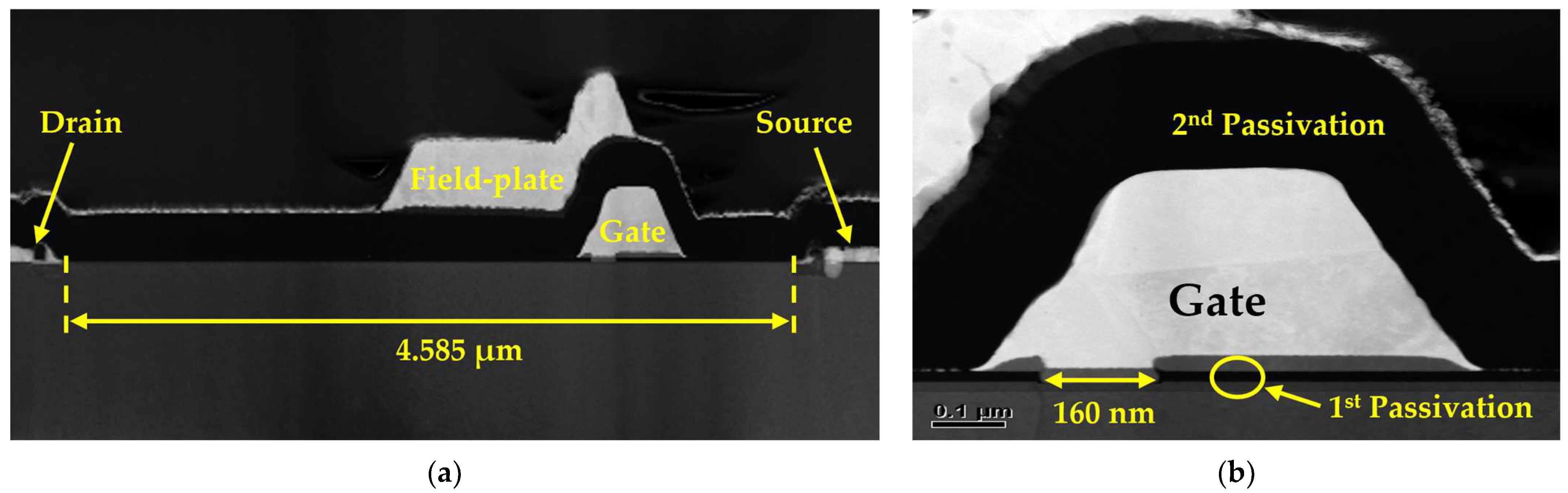
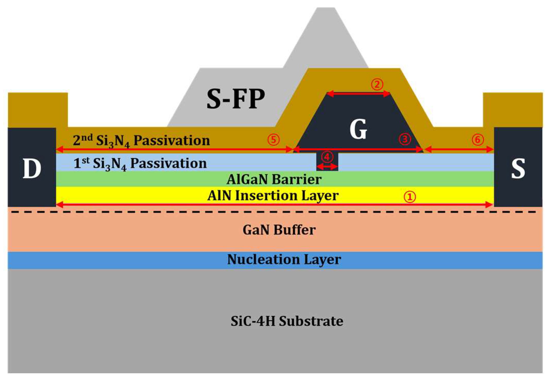
2. Materials and Methods

A 0.16 μm T-gate AlGaN/GaN HEMT was fabricated, and a cross-sectional view of the unit device is shown in Figure 1a. Figure 1b shows a magnified image of the gate electrode, featuring a 0.16 μm gate foot opening in the 1st passivation layer, which is covered on top by a 2nd passivation layer.
Figure 2 illustrates a cross-sectional view of a 0.16 μm T-gate AlGaN/GaN HEMT, which was used for technology computer-aided design (TCAD) modeling. In this figure, S is the source electrode, S-FP is the source-connected field plate, G is the gate electrode, and D is the drain electrode. The specific geometric parameters of the modeled device are listed in Table 1.
The AlGaN/GaN HEMT was grown on top of a 4-inch SiC-4H substrate using metal–organic chemical vapor deposition. The epitaxial layers were sequentially stacked and grown as follows: a 20 nm thick nucleation layer, a 1.04 μm thick Fe-doped GaN buffer layer, a 1 nm thick AlN insertion layer, and an 18 nm thick AlGaN barrier layer with 28% Al composition. The Ti/Au/Ni/Au alloyed ohmic contacts for the source and drain electrodes were formed by rapid thermal annealing at 775 °C for 30 s. Device isolation was achieved via P+ ion implantation. Subsequently, a 20 nm thick Si3N4 layer was deposited on the AlGaN barrier layer using plasma-enhanced chemical vapor deposition (PECVD). The first metal interconnection with the source and drain electrodes was established by Ti/Au evaporation after the etching of the 1st Si3N4 passivation layer. A planar gate was then created using single-layer electron beam lithography. A gate foot opening of 0.16 μm was achieved by exposing a polymethyl methacrylate resist to an electron beam, followed by the removal of the 1st Si3N4 passivation layer beneath the gate foot opening pattern through dry etching using inductively coupled plasma. The planar gate was defined using a Ni/Au metal stack deposited via electron–beam evaporation and subsequent lift-off processes. After defining the gate shape, a 250 nm thick 2nd Si3N4 passivation layer was deposited for device passivation using PECVD. The source-connected field plate (S-FP) was formed using a Ti/Au metal lift-off process. Finally, wafer thinning and backside via-hole processes were conducted [19].
To accurately predict the operational characteristics of a device, it is crucial to apply appropriate simulation parameters, such as electrical and thermal parameters, for each epitaxial layer. This meticulous approach ensures reliable and consistent simulation data. Consequently, the simulation parameters were meticulously calibrated to closely align with the actual device operating characteristics. For example, to mitigate the electron punch-through effect and reduce the substrate leakage current, iron (Fe) acceptor trap doping was leveraged in the GaN buffer layer to enhance the VBD [20]. In this simulation, a Gaussian acceptor doping profile was employed, with an acceptor doping concentration of 8.813 × 10¹⁴/cm3 at the AlGaN/GaN interface region and a peak trap concentration of 1018/cm3 [21]. In addition, a Selberherr impact ionization model was applied to simulate the VBD. Other simulation parameters such as electron mobility and heat models were accurately controlled to obtain reliable simulation results. The specific simulation parameters applied to the GaN and AlGaN layers are summarized in Table 2 [22].
After determining the appropriate simulation parameters, simulations were conducted to analyze the direct current (DC) and RF characteristics. The transconductance equation can be expressed as follows:
g m = I D S V G S ,
where g m , I D S , and V G S denote the transconductance, drain current, and gate voltage, respectively. The electric displacement was explained by Equation (2), as follows:
D = ε E ,
where D ,   ε , and E denote the electrical displacement, dielectric constant of the material, and electric field, respectively. Before evaluating the frequency characteristics of each structure, the relationship between the parasitic capacitances, such as CGS and CGD, and the frequency characteristics was investigated as follows:
C = ε A d ,
where A and d denote the overlapped area between two electrodes and the distance between the electrodes, respectively.
Next, fT can be determined using Equation (4), as follows:
f T = g m 2 π ( C G S + C G D ) g m 2 π C G S ,
where C G S and C G D denote the gate-to-source capacitance and gate-to-drain capacitance, respectively. As described in Equation (4), C G S and C G D have an inverse relationship with fT, which makes it crucial to minimize parasitic capacitances to maximize the frequency characteristics [23]. Therefore, we propose various dielectric passivation structures using materials with different dielectric constants, such as Si3N4, Al2O3, and HfO2, to analyze the RF characteristics related to capacitances. The specific material characteristics of these materials are summarized in Table 3 below [24,25].

3. Results

3.1. Matching Simulated and Measured Data for the Basic Si3N4 Entire Passivation Structure

To validate the simulation accuracy, a comparative analysis was conducted between the simulated and measured drain current–gate voltage (IDS-VGS) transfer characteristics of the fabricated Si3N4 EP structure device. The measured and simulated data exhibited close agreement in terms of IDS at VGS = 0 V (Idss), maximum transconductance (Gm), and threshold voltage (Vth). Figure 3a compares the measured and simulated IDS-VGS transfer characteristics. The measured and simulated Idss values were 817.10 and 811.99 mA/mm, respectively. Similarly, the measured and simulated maximum transconductance values were 400.39 and 397.65 mS/mm, respectively. Furthermore, the measured Vth was −3.1 V, and the simulated value was −3 V. These results confirm a close match between the measured and simulated data for Idss, Gm, and Vth with error rates of 0.6%, 0.7%, and 3.2%, respectively.
The measured and simulated fT values of the basic Si3N4 EP structure are shown in Figure 3b. The RF characteristics were evaluated under VDS = 10 V and VGS = −2 V conditions for both measurement and simulation. More specifically, fT was defined as the intersection of the extension line at the current gain point (H21) with the x-axis with a slope of −20 dB/decade [26]. The measured and simulated fT values were 29.26 and 29.51 GHz, respectively, demonstrating excellent agreement with the minimal error rate of 0.9%.

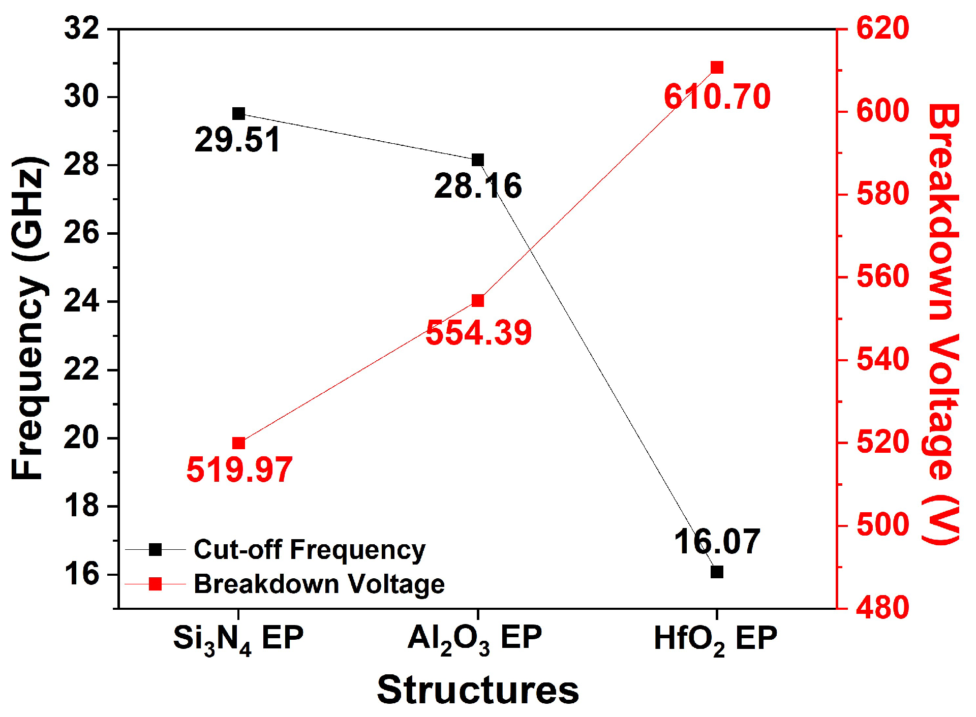
3.2. Comparative Analysis of Entire Passivation Structures Based on Dielectric Materials

To accommodate high-power applications, the passivation layer of the Si3N4 EP structure was replaced with a high-k material. Two distinct dielectric materials were modeled (Al2O3 and HfO2) for the EP structure, as shown in Figure 4. All structural parameters except for the passivation material remained unchanged during the simulation.

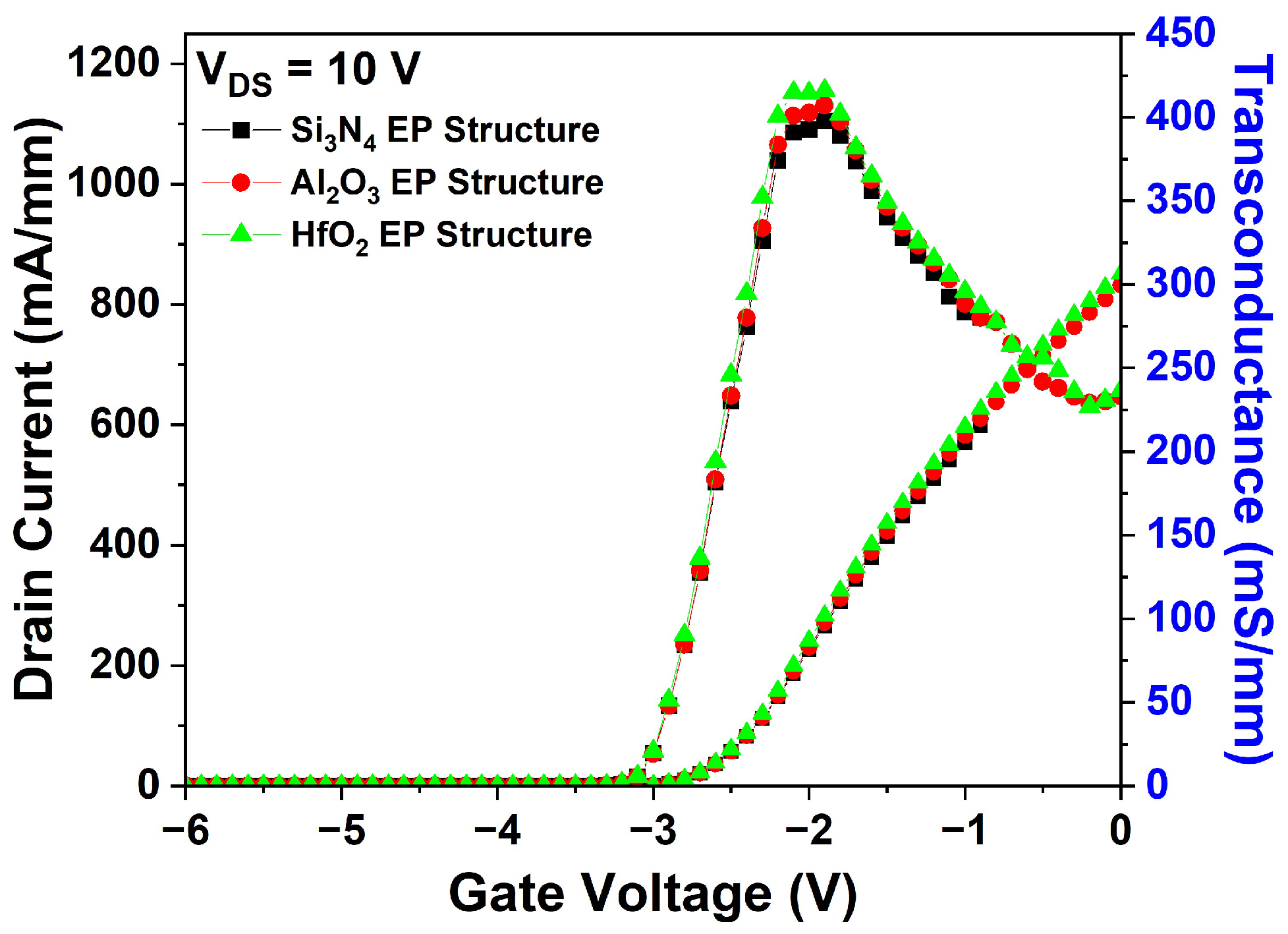
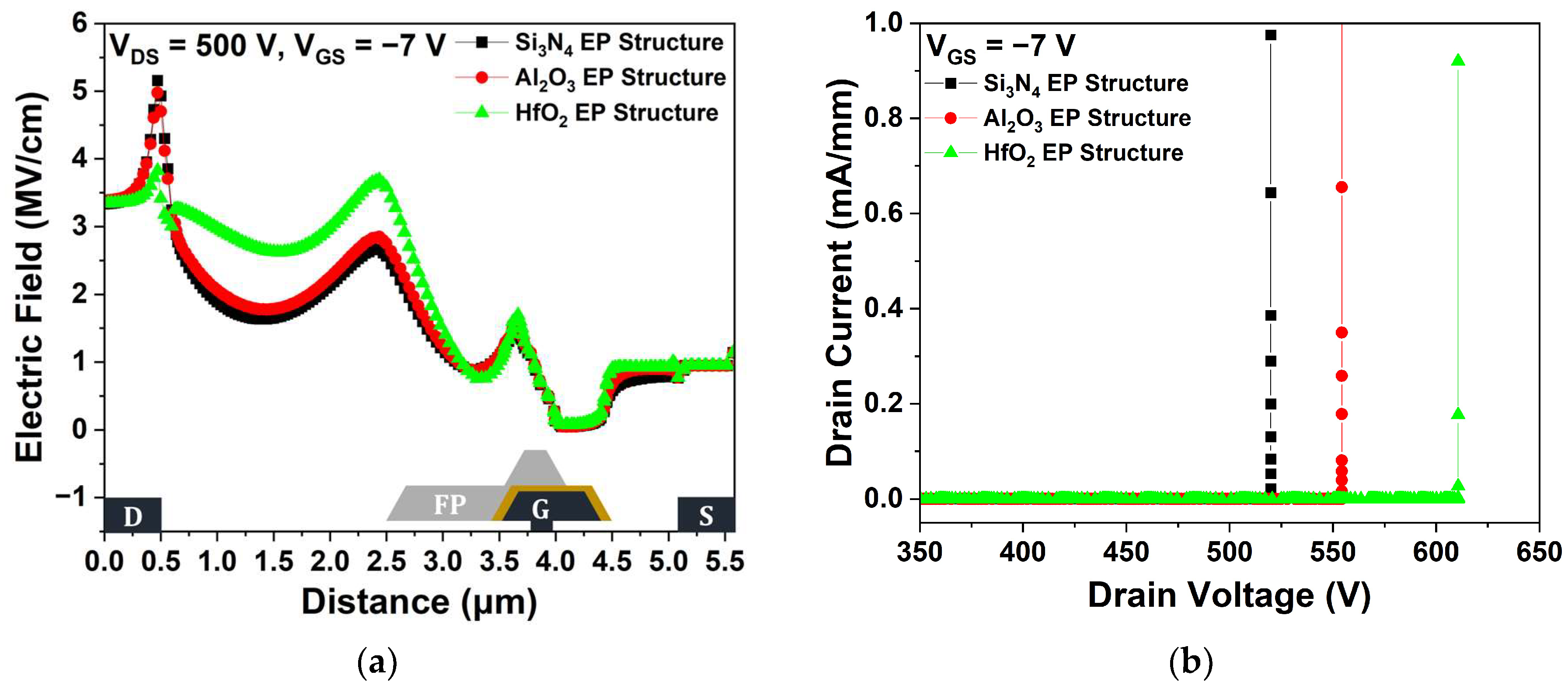
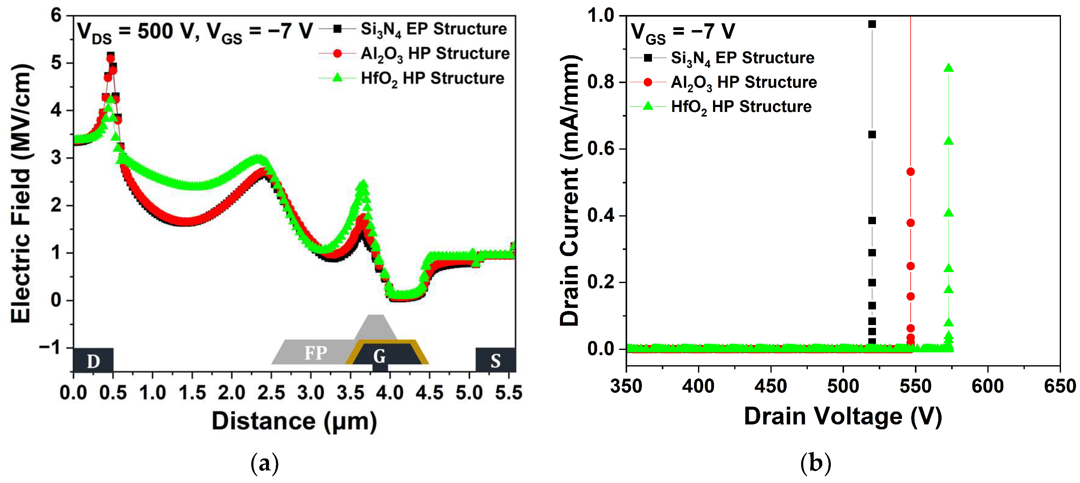
3.2.1. Simulation Results of the DC Characteristics

The DC characteristics of the Al2O3 and HfO2 EP structures were compared with those of the basic Si3N4 EP structure. Figure 5 shows the IDS-VGS transfer characteristics of the three structures at VDS = 10 V. No significant variations in the IDS were observed, and the Vth remained constant at −3.0 V.
Figure 6a shows the electric field distributions within the channel layer at VDS = 500 V for the three passivation structures. Compared with the Si3N4 EP structure, the Al2O3 and HfO2 EP structures exhibited more efficient electric field dispersion, resulting in a lower maximum electric field in the channel layer due to their high dielectric constant. As the maximum electric field increased, the impact ionization that caused the generation of electron–hole pairs was enhanced; therefore, electric field redistribution effectively improved VBD [27]. The dielectric constant of Al2O3 is lower than that of HfO2, resulting in a relatively lower VBD [28]. The VBD characteristics were simulated under a VGS = −7 V pinch-off condition to ensure a completely off device state. We defined VBD as the VDS when the IDS exceeded 1 mA/mm after completely turning off the device by applying a voltage of −7 V across the gate. As shown in Figure 6b, the Si3N4, Al2O3, and HfO2 EP structures exhibited VBD values of 519.97, 554.39, and 610.70 V, respectively. The VBD of the Al2O3 and HfO2 EP structures were improved by 6.62% and 17.45%, respectively, compared with that of the Si3N4 EP structure.

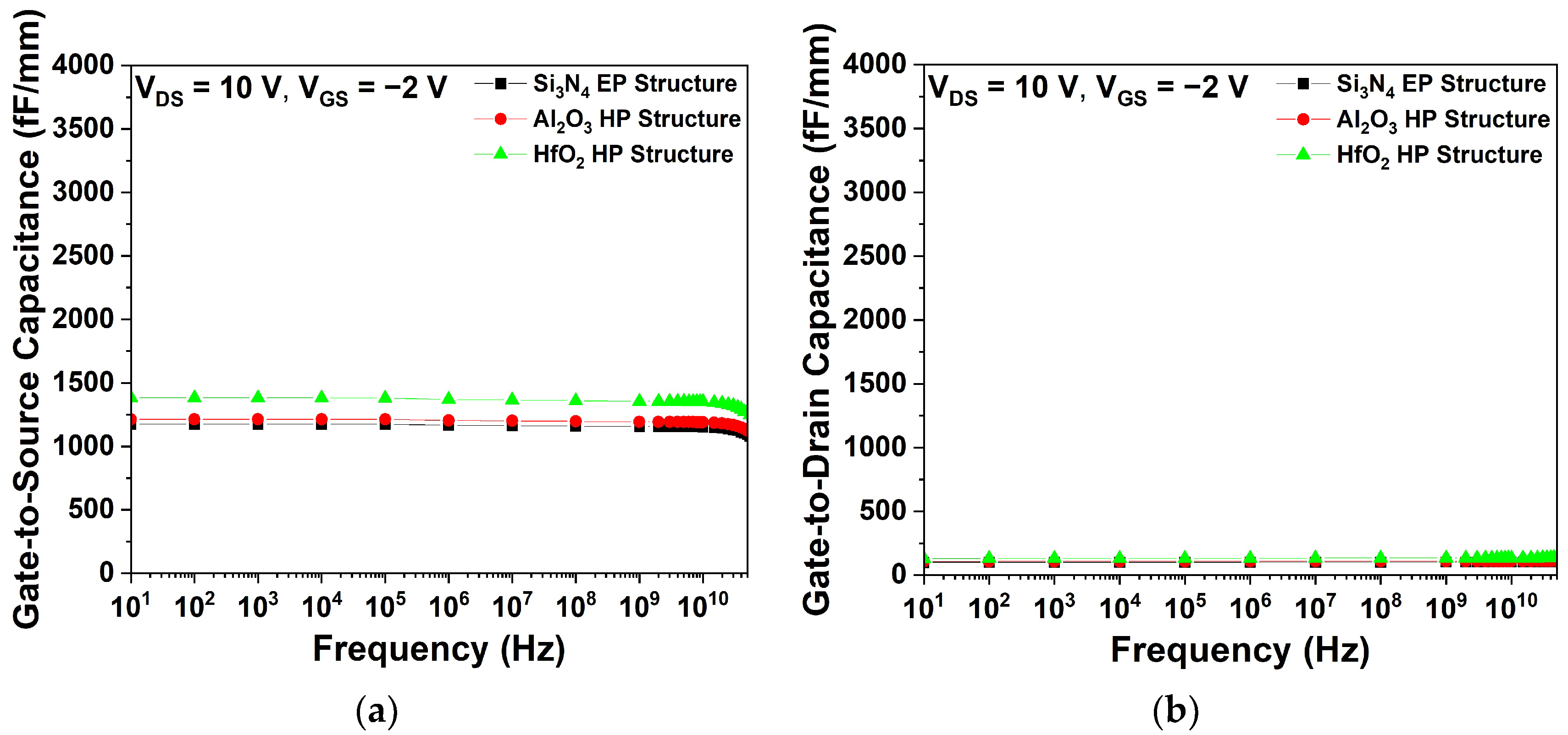
3.2.2. Simulation Results of the RF Characteristics

Figure 7 shows the parasitic capacitance characteristics of the Si3N4, Al2O3, and HfO2 EP structures. As shown in Figure 7a,b, the CGS and CGD were determined at VDS = 10 V and VGS = −2 V. The HfO2 EP structure exhibited the highest CGS and CGD values, which can be attributed to the dielectric constant of HfO2, as described by Equation (3). Conversely, the Al2O3 EP structure exhibited lower parasitic capacitance values than the HfO2 EP structure, due to its lower dielectric constant.
Figure 8 shows the simulated fT and VBD values for the three EP structures. fT simulations were conducted at VDS = 10 V and VGS = −2 V. According to Equation (4), the fT values of the three EP structures were affected by transconductance (gm) and CGS. The Si3N4, Al2O3, and HfO2 EP structures exhibited fT values of 29.51, 28.16, and 16.07 GHz, respectively. Compared with the Si3N4 EP structure, the Al2O3 and HfO2 EP structures exhibited reductions of 4.57% and 45.54%, respectively.

3.2.3. Simulation Results of the Hybrid Passivation Structure

To address the trade-off between enhanced VBD values and degraded fT associated with the application of Al2O3 and HfO2 to the EP structures, HP structures were proposed by employing Al2O3 and HfO2 into the 1st passivation and Si3N4 into the 2nd passivation. Figure 9 shows the schematics of the HP structures with Al2O3 and HfO2.
Figure 10a shows the electric field distributions for three different structures. The maximum electric fields of the Al2O3 and HfO2 HP structures were lower than those of the basic Si3N4 EP structure. The dielectric constant of Al2O3 is lower than that of HfO2, resulting in a relatively lower VBD. Specifically, the VBD values of the Al2O3 and HfO2 HP structures were 546.39 and 572.87 V, respectively, as shown in Figure 10b. However, compared with the EP structure, the HP structure exhibited a reduced VBD because of the use of a high-k material only for the 1st passivation.
Figure 11 shows the parasitic capacitance characteristics of the different 1st passivation materials. Given that LGate-Source was shorter than LGate-Drain, CGS exhibited a larger value than CGD, indicating that the capacitance was affected by the distance between the electrodes [29]. Figure 11 shows that the HfO2 HP structure exhibited the highest CGS and CGD values. Conversely, the Al2O3 HP structure exhibited lower parasitic capacitance values than the HfO2 HP structure, which was due to the relatively low dielectric constant of Al2O3.
Figure 12 compares the simulated fT values for the three dielectric passivation structures. Simulations conducted at VDS = 10 V and VGS = −2 V revealed fT values of 28.63 and 26.46 GHz for the Al2O3 and HfO2 HP structures, respectively. Compared with the Si3N4 EP structure, these values represent fT reductions of 2.98% and 10.34% for the HfO2 and Al2O3 HP structures, respectively. According to Equation (4), the decrease in fT can be attributed to the increase in CGS. Compared to the high-k EP structure, the HP structure compensated for the decrease in RF characteristics by applying a high-k material only at the 1st passivation layer.

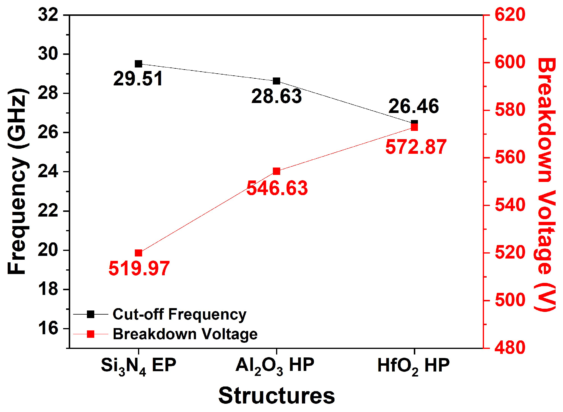
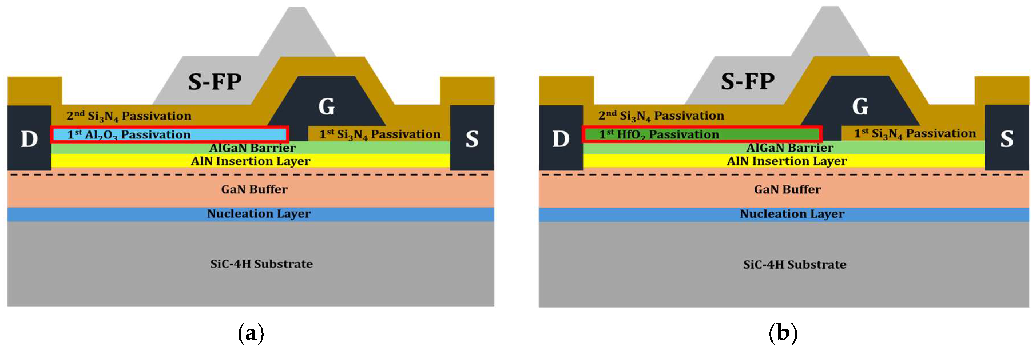
3.3. Comparative Analysis of Partial Passivation Structures Based on Al2O3 and HfO2

To mitigate the degradation of the RF characteristics observed in the HP structure while preserving the benefits of high-k materials, a PP structure was introduced. By implementing the HP structure, the RF characteristics were improved compared to the high-k EP structure. However, the fT of the HP structure was lower than that of the basic Si3N4 EP structure. To minimize the degradation of the RF characteristics, we applied the PP structure with a high-k material only for the 1st passivation layer at the drain-gate region. Figure 13 shows schematic diagrams of the PP structure with Al2O3 and HfO2.

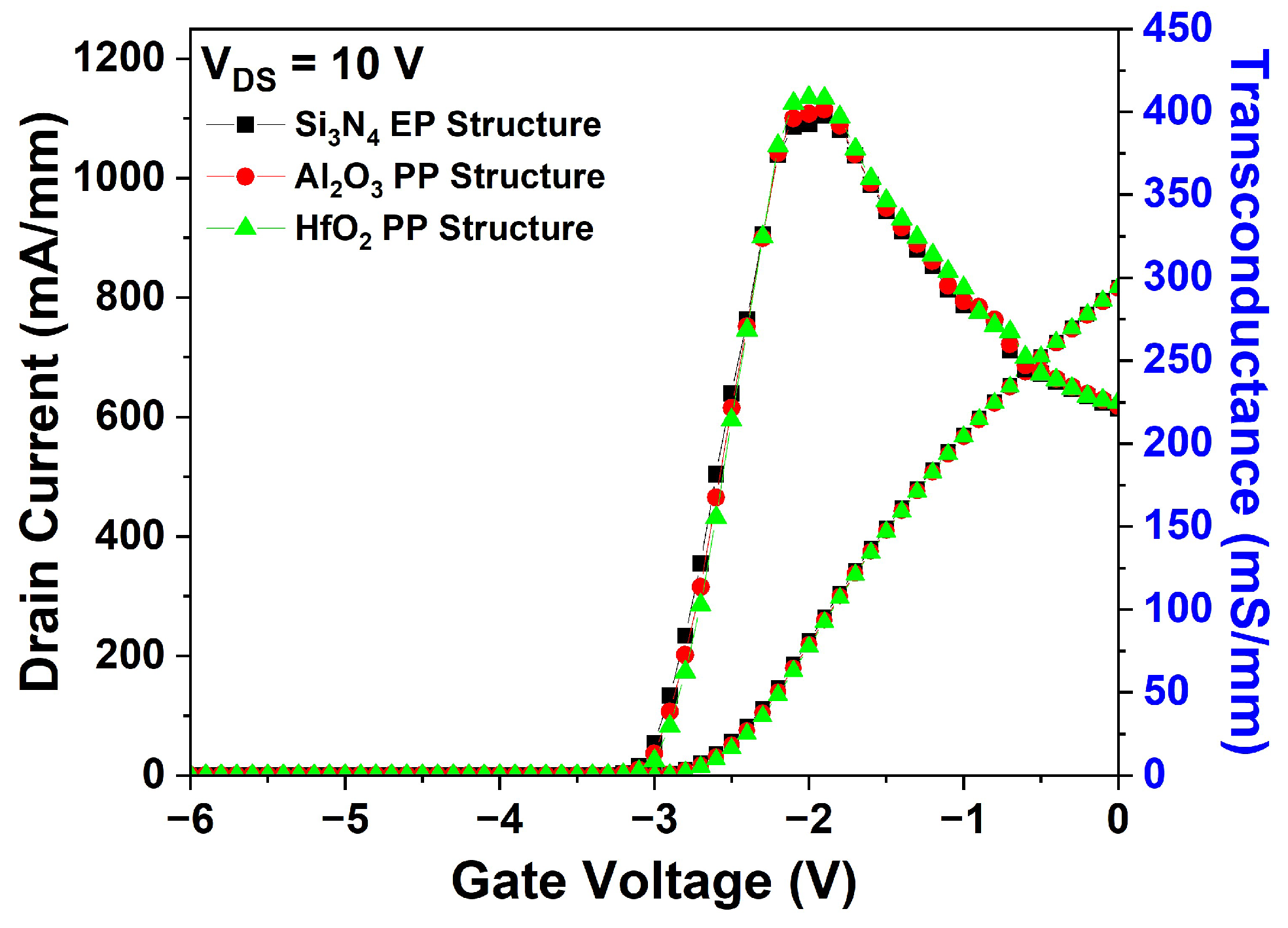
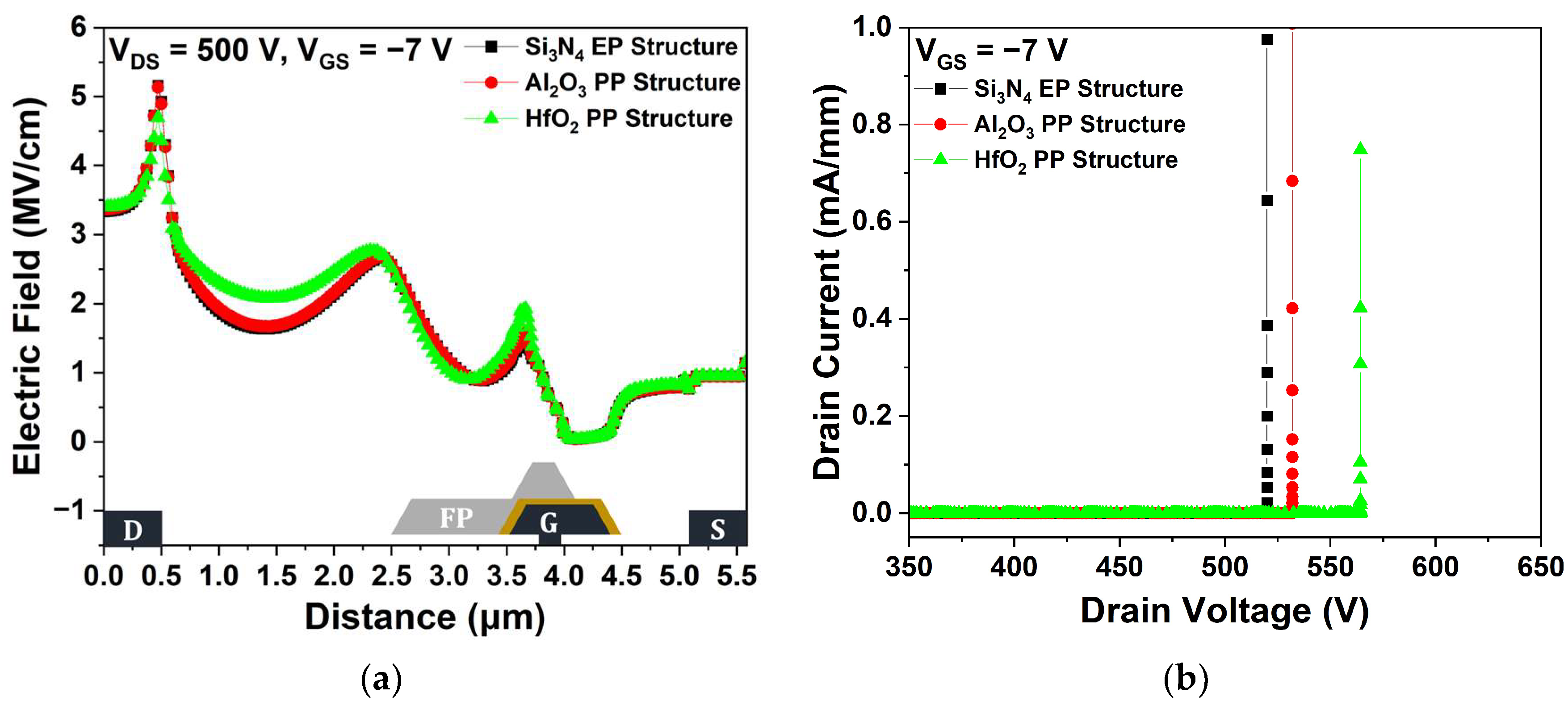
3.3.1. Simulation Results of the DC Characteristics

The IDS-VGS transfer characteristics, electric field distribution, and VBD characteristics of the Al2O3 and HfO2 PP structures were simulated. As shown in Figure 14, the IDS, gm, and Vth values remained unaffected by variations in the material of the 1st passivation layer at the drain–gate region.
Figure 15a shows that the maximum electric field for the HfO2 PP structure, which exhibited the highest dielectric constant, decreased and was dispersed in the drain–gate region. Conversely, the lower dielectric constant of Al2O3 in the Al2O3 PP structure resulted in less pronounced electric field dispersion. Figure 15b shows that the VBD of the HfO2 PP structure exhibited the highest VBD value of 564.27 V, while the Si3N4 EP and Al2O3 PP structures exhibited comparable values of 519.97 and 532.08 V, respectively. Notably, the use of a high-k material as the 1st passivation layer at the drain–gate region, where the electric field peak occurs, resulted in a slight decrease in VBD for the PP structure compared to the HP structure.

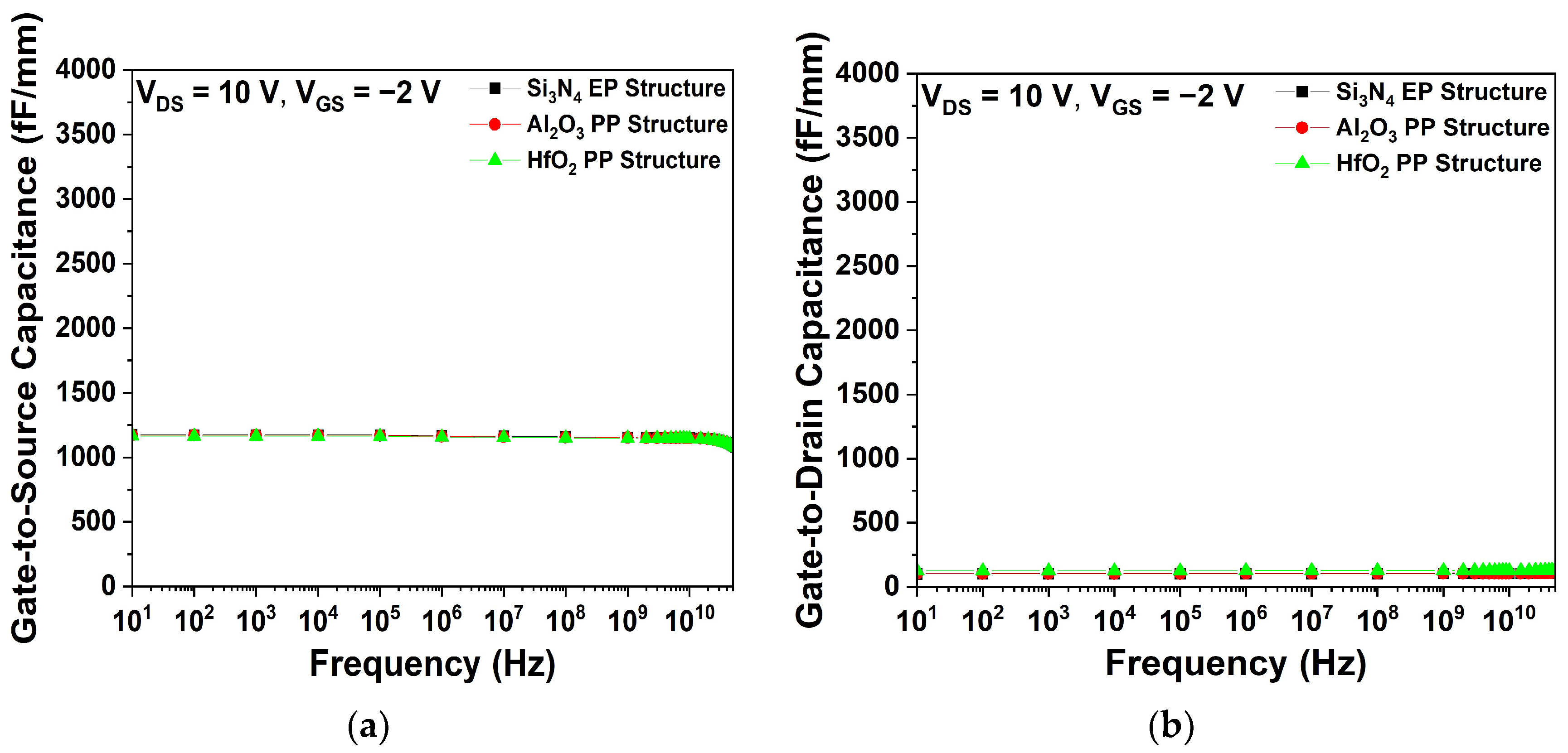
3.3.2. Simulation Results of the RF Characteristics

Figure 16 shows the parasitic capacitance characteristics of the Si3N4 EP, HfO2, and Al2O3 PP structures. Given that all three structures employed Si3N4 as a passivation layer at the source–gate region, the CGS remained consistent, as shown in Figure 16a. However, Figure 16b shows that the HfO2 PP structure exhibits the highest CGD value.
Figure 17 shows the simulated fT values for different dielectric passivation structures at VDS = 10 V and VGS = −2 V. Notably, the fT values of the Si3N4 EP, Al2O3 HP, and HfO2 HP structures exhibited minimal variations (29.51, 29.44, and 29.37 GHz, respectively). Equation (4) indicates that fT is primarily influenced by CGS, and a negligible change in CGS results in the observed fT consistency. These results highlight the effectiveness of the PP structure in mitigating the degradation of the RF characteristics.

4. Discussion

This study simulates and analyzes the DC and RF characteristics of various dielectric passivation structures. Table 4 summarizes the DC and RF characteristics, including JFOM, for seven different dielectric passivation structures of the AlGaN/GaN HEMT. Among the Si3N4, Al2O3, and HfO2 EP structures, the HfO2 EP structure exhibited the highest VBD. However, the high-k passivation layer inevitably entailed a decrease in fT due to parasitic capacitance. To minimize the degradation of fT, HP and PP structures were applied. The JFOM was calculated to analyze the trade-off relationship between VBD and fT. The basic Si3N4 EP structure has a JFOM of 15.34 THz-V. The JFOMs with three different Al2O3 passivation structures were not significantly different from the Si3N4 EP structure. However, the proposed HfO2 PP structure exhibited the highest JFOM of 16.75 THz-V with enhanced VBD while maintaining fT.

5. Conclusions

This study investigates the DC and RF characteristics of AlGaN/GaN HEMTs using various passivation material configurations via TCAD simulation. The simulation parameters were obtained by matching the simulation data with the measured data of a fabricated basic Si3N4 EP structure of HEMT to ensure the reliability of the simulation results. The JFOM was calculated to assess the operational characteristics of each proposed dielectric passivation structure considering the trade-off between the breakdown voltage and cut-off frequency. Consequently, based on the highest calculated JFOM among the investigated structures, the HfO2 PP structure was proposed as the optimal dielectric passivation structure for achieving superior breakdown voltage and frequency characteristics. This structure shows promise for high-power and high-frequency AlGaN/GaN HEMT applications.

Author Contributions

Conceptualization and writing—original draft preparation, J.-H.K.; software and investigation, C.-Y.L.; formal analysis and data curation, J.-H.L.; validation and formal analysis, J.-H.C.; formal analysis and investigation, B.-G.M.; validation and investigation, D.M.K.; supervision, funding acquisition, resources, and writing—review and editing, H.-S.K. All authors have read and agreed to the published version of the manuscript.

Funding

This work was partly supported by an Institute of Information & Communications Technology Planning & Evaluation (IITP) grant funded by the government of the Republic of Korea (MSIT) under grant No. 2021-0-00760, as well as the Institute of Civil Military Technology Cooperation, funded by the Defense Acquisition Program Administration and the Ministry of Trade, Industry and Energy of the government of the Republic of Korea, under grant No. 22-CM-15.

Data Availability Statement

Data are contained within the article.

Conflicts of Interest

The authors declare no conflicts of interest.

References

  1. Mishra, U.K.; Parikh, P.; Wu, Y.F. AlGaN/GaN HEMTs—An overview of device operation and applications. Proc. IEEE 2002, 90, 1022–1031. [Google Scholar] [CrossRef]
  2. Hamza, K.H.; Nirmal, D. A review of GaN HEMT broadband power amplifiers. AEU-Int. J. Electron. Commun. 2020, 116, 153040. [Google Scholar] [CrossRef]
  3. Levinshtein, M.E.; Rumyantsev, S.L.; Shur, M.S. (Eds.) Properties of Advanced Semiconductor Materials: GaN, AIN, InN, BN, SiC, SiGe; John Wiley & Sons: Hoboken, NJ, USA, 2001. [Google Scholar]
  4. Lenka, T.R.; Panda, A.K. Characteristics study of 2DEG transport properties of AlGaN/GaN and AlGaAs/GaAs-based HEMT. Semiconductors 2011, 45, 650–656. [Google Scholar] [CrossRef]
  5. Kranti, A.; Haldar, S.; Gupta, R.S. An accurate charge control model for spontaneous and piezoelectric polarization dependent two-dimensional electron gas sheet charge density of lattice-mismatched AlGaN/GaN HEMTs. Solid-State Electron. 2002, 46, 621–630. [Google Scholar]
  6. Sanyal, I.; Lin, E.S.; Wan, Y.C.; Chen, K.M.; Tu, P.T.; Yeh, P.C.; Chyi, J.I. AlInGaN/GaN HEMTs with high Johnson’s figure-of-merit on low resistivity silicon substrate. IEEE J. Electron. Devices Soc. 2020, 9, 130–136. [Google Scholar] [CrossRef]
  7. Augustine Fletcher, A.S.; Nirmal, D.; Arivazhagan, L.; Ajayan, J.; Varghese, A. Enhancement of Johnson figure of merit in III-V HEMT combined with discrete field plate and AlGaN blocking layer. Int. J. RF Microw. Comput.-Aided Eng. 2020, 30, e22040. [Google Scholar] [CrossRef]
  8. Liu, C.; Chor, E.F.; Tan, L.S. Enhanced device performance of AlGaN/GaN HEMTs using HfO2 high-k dielectric for surface passivation and gate oxide. Semicond. Sci. Technol. 2007, 22, 522. [Google Scholar] [CrossRef]
  9. Koveshnikov, S.; Tsai, W.; Ok, I.; Lee, J.C.; Torkanov, V.; Yakimov, M.; Oktyabrsky, S. Metal-oxide-semiconductor capacitors on GaAs with high-k gate oxide and amorphous silicon interface passivation layer. Appl. Phys. Lett. 2006, 88, 022106. [Google Scholar] [CrossRef]
  10. Kumar, M.; Gupta, S.; Venkataraman, V. Compact modeling of the effects of parasitic internal fringe capacitance on the threshold voltage of high-k gate-dielectric nanoscale SOI MOSFETs. IEEE Trans. Electron. Devices 2006, 53, 706–711. [Google Scholar] [CrossRef]
  11. Hanawa, H.; Onodera, H.; Nakajima, A.; Horio, K. Numerical Analysis of Breakdown Voltage Enhancement in AlGaN/GaN HEMTs With a High-k Passivation Layer. IEEE Trans. Electron. Devices 2014, 61, 769–775. [Google Scholar] [CrossRef]
  12. Jebalin, B.K.; Rekh, A.S.; Prajoon, P.; Kumar, N.; Nirmal, D. The influence of high-k passivation layer on breakdown voltage of Schottky AlGaN/GaN HEMTs. Microelectron. J. 2015, 46, 1387–1391. [Google Scholar] [CrossRef]
  13. Chander, S.; Gupta, S.; Gupta, M. Enhancement of breakdown voltage in AlGaN/GaN HEMT using passivation technique for microwave application. Superlattices Microstruct. 2018, 120, 217–222. [Google Scholar] [CrossRef]
  14. Choi, J.H.; Kang, W.S.; Kim, D.; Kim, J.H.; Lee, J.H.; Kim, K.Y.; Min, B.G.; Kang, D.M.; Kim, H.S. Enhanced operational characteristics attained by applying HfO2 as passivation in AlGaN/GaN high-electron-mobility transistors: A simulation study. Micromachines 2023, 14, 1101. [Google Scholar] [CrossRef] [PubMed]
  15. Liu, X.; Qin, J.; Chen, J.; Chen, J.; Wang, H. Novel stacked passivation structure for AlGaN/GaN HEMTs on silicon with high Johnson’s figures of merit. IEEE J. Electron Devices Soc. 2023, 11, 130–134. [Google Scholar] [CrossRef]
  16. Du, J.; Chen, N.; Pan, P.; Bai, Z.; Li, L.; Mo, J.; Yu, Q. High breakdown voltage AlGaN/GaN HEMT with high-K/low-K compound passivation. Electron. Lett. 2015, 51, 104–106. [Google Scholar] [CrossRef]
  17. Prasannanjaneyulu, B.; Karmalkar, S. Relative effectiveness of high-k passivation and gate-connected field plate techniques in enhancing GaN HEMT breakdown. Microelectron. Reliab. 2020, 110, 113698. [Google Scholar] [CrossRef]
  18. Wu, J.; Xu, C.; Fan, Y.; Liu, X.; Zhong, Z.; Yin, J.; Zhang, C.; Li, J.; Kang, J. TCAD study of high breakdown voltage AlGaN/GaN HEMTs with embedded passivation layer. J. Phys. D Appl. Phys. 2022, 55, 384001. [Google Scholar] [CrossRef]
  19. Yoon, H.S.; Min, B.G.; Lee, J.M.; Kang, D.M.; Ahn, H.K.; Kim, H.; Lim, J. Microwave Low-Noise Performance of 0.17 μm Gate-Length AlGaN/GaN HEMTs on SiC With Wide Head Double-Deck T-Shaped Gate. IEEE Electron Device Lett. 2016, 37, 1407–1410. [Google Scholar] [CrossRef]
  20. Ma, M.; Cao, Y.; Lv, H.; Wang, Z.; Zhang, X.; Chen, C.; Wu, L.; Lv, L.; Zheng, X.; Tian, W.; et al. Effect of acceptor traps in GaN buffer layer on breakdown performance of AlGaN/GaN HEMTs. Micromachines 2022, 14, 79. [Google Scholar] [CrossRef]
  21. Kang, W.-S.; Choi, J.-H.; Kim, D.; Kim, J.-H.; Lee, J.-H.; Min, B.-G.; Kang, D.M.; Choi, J.H.; Kim, H.-S. Optimization of gate-head-top/bottom lengths of AlGaN/GaN high-electron-mobility transistors with a gate-recessed structure for high-power operations: A simulation study. Micromachines 2023, 15, 57. [Google Scholar] [CrossRef]
  22. Silvaco, Inc. Material Dependent Physical Models. In Atlas User’s Manual Device Simulation Software; Silvaco Inc.: Santa Clara, CA, USA, 2016; pp. 519–523. [Google Scholar]
  23. Majumder, A.; Chatterjee, S.; Chatterjee, S.; Chaudhari, S.S.; Poddar, D.R. Optimization of small-signal model of GaN HEMT by using evolutionary algorithms. IEEE Microw. Wirel. Compon. Lett. 2017, 27, 362–364. [Google Scholar] [CrossRef]
  24. Clark, R.D. Emerging applications for high K materials in VLSI technology. Materials 2014, 7, 2913–2944. [Google Scholar] [CrossRef] [PubMed]
  25. Chang, Y.C.; Huang, M.L.; Chang, Y.H.; Lee, Y.J.; Chiu, H.C.; Kwo, J.; Hong, M. Atomic-layer-deposited Al2O3 and HfO2 on GaN: A comparative study on interfaces and electrical characteristics. Microelectron. Eng. 2011, 88, 1207–1210. [Google Scholar] [CrossRef]
  26. Yoon, H.S.; Min, B.G.; Lee, J.M.; Kang, D.M.; Ahn, H.K.; Kim, H.C.; Lim, J.W. Wide head T-shaped gate process for low-noise AlGaN/GaN HEMTs. In Proceedings of the CS MANTECH Conference, Scottsdale, AZ, USA, 18–21 May 2015; pp. 18–21. [Google Scholar]
  27. Selberherr, S. MOS device modeling at 77 K. IEEE Trans. Electron. Devices 1989, 36, 1464–1474. [Google Scholar] [CrossRef]
  28. Hanawa, H.; Satoh, Y.; Horio, K. Effects of buffer leakage current on breakdown characteristics in AlGaN/GaN HEMTs with a high-k passivation layer. Microelectron. Eng. 2015, 147, 96–99. [Google Scholar] [CrossRef]
  29. Lee, J.H.; Choi, J.H.; Kang, W.S.; Kim, D.; Min, B.G.; Kang, D.M.; Choi, J.H.; Kim, H.S. Analysis of Operational Characteristics of AlGaN/GaN High-Electron-Mobility Transistor with Various Slant-Gate-Based Structures: A Simulation Study. Micromachines 2022, 13, 1957. [Google Scholar] [CrossRef]
Figure 1. Transmission electron microscope images of the fabricated 0.16 μm gate foot length of the basic Si3N4 entire passivation (EP) high-electron-mobility transistor (HEMT): (a) a cross-sectional view of the unit device and (b) an enlarged image of the gate electrode.
Micromachines 15 01126 g001
Figure 2. An illustration of 0.16 μm gate foot length of the basic Si3N4 EP HEMT used for TCAD modeling. S-FP stands for source-connected field plate. G, D, and S stand for gate, drain, and source, respectively.
Micromachines 15 01126 g002
Figure 3. Measured and simulated results of the basic Si3N4 EP HEMT: (a) drain current–gate voltage (IDS-VGS) transfer characteristics at drain voltage (VDS) = 10 V; (b) cut-off frequency (fT) at VDS = 10 V and gate voltage (VGS) = −2 V.
Micromachines 15 01126 g003
Figure 4. Illustrations of EP structures: (a) with Al2O3; (b) with HfO2. S-FP stands for source-connected field plate. G, D, and S stand for gate, drain, and source, respectively.
Micromachines 15 01126 g004
Figure 5. Simulation results of IDS-VGS transfer characteristics for the three EP structures at VDS = 10 V.
Micromachines 15 01126 g005
Figure 6. (a) Electric field distributions across the 2-DEG (2-dimensional electron gas) channel layer between the source and drain electrodes at VDS = 500 V and VGS = −7 V; (b) breakdown voltage (VBD) at pinch-off (VGS = −7 V).
Micromachines 15 01126 g006
Figure 7. Simulated capacitance characteristics as a function of frequency for three different EP structures at VDS = 10 V and VGS = −2 V; (a) gate-to-source capacitance (CGS) and (b) gate-to-drain capacitance (CGD).
Micromachines 15 01126 g007
Figure 8. Simulated fT and VBD for three different EP structures.
Micromachines 15 01126 g008
Figure 9. Illustrations of hybrid passivation (HP) structures: (a) with Al2O3; (b) with HfO2.
Micromachines 15 01126 g009
Figure 10. Comparison of Si3N4 EP, Al2O3 HP, and HfO2 HP structures: (a) electric field distributions across the 2-DEG channel layer between the source and drain electrodes at VDS = 500 V and VGS = −7 V; (b) VBD at pinch-off (VGS = −7 V).
Micromachines 15 01126 g010
Figure 11. Simulated capacitance characteristics as a function of frequency for Si3N4 EP, Al2O3 HP, and HfO2 HP structures at VDS = 10 V and VGS = −2 V; (a) CGS and (b) CGD.
Micromachines 15 01126 g011
Figure 12. Simulated fT and VBD values for the Si3N4 EP, Al2O3 HP, and HfO2 HP structures.
Micromachines 15 01126 g012
Figure 13. Illustrations of partial passivation (PP) structures: (a) with Al2O3; (b) with HfO2.
Micromachines 15 01126 g013
Figure 14. Simulation results of IDS-VGS transfer characteristics in the Si3N4 EP, Al2O3 PP, and HfO2 PP structures.
Micromachines 15 01126 g014
Figure 15. Comparison of Si3N4 EP, Al2O3 PP, and HfO2 PP structures: (a) electric field distributions across the 2-DEG channel layer between the source and drain electrodes at VDS = 500 V and VGS = −7 V; (b) VBD at pinch-off (VGS = −7 V).
Micromachines 15 01126 g015
Figure 16. Simulated capacitance characteristics as a function of frequency for Si3N4 EP, Al2O3 PP, and HfO2 PP structures at VDS = 10 V and VGS = −2 V; (a) CGS and (b) CGD.
Micromachines 15 01126 g016
Figure 17. Simulated fT and VBD for Si3N4 EP, Al2O3 PP, and HfO2 PP structures.
Micromachines 15 01126 g017
Table 1. Specific geometric parameters of the 0.16 μm gate foot length of the basic Si3N4 EP HEMT.
ParametersValue (μm)
① LSource-Drain4.585
② LGate-Head-Top0.26
③ LGate-Head-Bottom0.71
④ LGate-Foot0.16
⑤ LGate-Drain3.175
⑥ LGate-Source0.7
SiC-4H substrate5
Nucleation layer0.02
GaN buffer1.04
AlN insertion layer0.001
AlGaN barrier0.018
1st passivation0.02
2nd passivation0.25
Table 2. Material parameters for the simulation at a room temperature.
ParametersUnitsGaNAlGaN
Bandgap energyeV3.393.88
Electron affinityeV4.22.3
Dielectric constant-9.59.38
Low-field electron mobility-Farahmand modified Caughey–Thomas Model
High-field electron mobility-GANSAT Model
Electron saturation velocitycm/s1.9 × 1071.12 × 107
Hole saturation velocitycm/s1.9 × 1071.00 × 106
Electron Shockley–Read–Hall lifetimes1.0 × 10−81.0 × 10⁻⁸
Hole Shockley–Read–Hall lifetimes1.0 × 10−81.0 × 10⁻⁸
Table 3. Material characteristics of Si3N4, Al2O3, and HfO2.
ParametersUnitsSi3N4Al2O3HfO2
Dielectric constant-~7.5~9~25
Bandgap energyeV5.37.15.8
Table 4. A summary of DC and RF characteristics of various dielectric passivation structures of HEMT.
ParametersUnitsSi3N4Al2O3HfO2
Structure type-EPEPHPPPEPHPPP
Peak electric fieldMV/cm5.164.985.095.133.834.224.69
Breakdown voltage (VBD)V519.97554.39546.63532.08610.70572.87564.27
Cut-off frequency (fT)GHz29.5128.1628.6329.4416.0726.4629.37
Johnson’s figure-of-merit (JFOM)THz-V15.3415.6315.6515.669.8115.1616.75
Disclaimer/Publisher’s Note: The statements, opinions and data contained in all publications are solely those of the individual author(s) and contributor(s) and not of MDPI and/or the editor(s). MDPI and/or the editor(s) disclaim responsibility for any injury to people or property resulting from any ideas, methods, instructions or products referred to in the content.

